EP0199282A2 - Convertisseur numérique-analogique interpolatif - Google Patents
Convertisseur numérique-analogique interpolatif Download PDFInfo
- Publication number
- EP0199282A2 EP0199282A2 EP86105283A EP86105283A EP0199282A2 EP 0199282 A2 EP0199282 A2 EP 0199282A2 EP 86105283 A EP86105283 A EP 86105283A EP 86105283 A EP86105283 A EP 86105283A EP 0199282 A2 EP0199282 A2 EP 0199282A2
- Authority
- EP
- European Patent Office
- Prior art keywords
- signal
- digital
- output
- arithmetic circuit
- feedback signal
- Prior art date
- Legal status (The legal status is an assumption and is not a legal conclusion. Google has not performed a legal analysis and makes no representation as to the accuracy of the status listed.)
- Granted
Links
- 238000005070 sampling Methods 0.000 abstract description 8
- 238000013139 quantization Methods 0.000 abstract description 5
- 239000003990 capacitor Substances 0.000 description 10
- 238000010586 diagram Methods 0.000 description 7
- 238000003491 array Methods 0.000 description 5
- 238000004364 calculation method Methods 0.000 description 5
- 238000006243 chemical reaction Methods 0.000 description 5
- 238000000034 method Methods 0.000 description 4
- 238000004891 communication Methods 0.000 description 2
- 230000000116 mitigating effect Effects 0.000 description 2
- 239000004065 semiconductor Substances 0.000 description 2
- 230000000295 complement effect Effects 0.000 description 1
- 239000000470 constituent Substances 0.000 description 1
- 230000008094 contradictory effect Effects 0.000 description 1
- 230000000694 effects Effects 0.000 description 1
- 238000011156 evaluation Methods 0.000 description 1
- 230000002349 favourable effect Effects 0.000 description 1
- 238000007493 shaping process Methods 0.000 description 1
Images


Classifications
-
- H—ELECTRICITY
- H03—ELECTRONIC CIRCUITRY
- H03M—CODING; DECODING; CODE CONVERSION IN GENERAL
- H03M7/00—Conversion of a code where information is represented by a given sequence or number of digits to a code where the same, similar or subset of information is represented by a different sequence or number of digits
- H03M7/30—Compression; Expansion; Suppression of unnecessary data, e.g. redundancy reduction
- H03M7/3002—Conversion to or from differential modulation
- H03M7/3004—Digital delta-sigma modulation
- H03M7/3015—Structural details of digital delta-sigma modulators
- H03M7/3031—Structural details of digital delta-sigma modulators characterised by the order of the loop filter, e.g. having a first order loop filter in the feedforward path
-
- H—ELECTRICITY
- H03—ELECTRONIC CIRCUITRY
- H03M—CODING; DECODING; CODE CONVERSION IN GENERAL
- H03M3/00—Conversion of analogue values to or from differential modulation
- H03M3/30—Delta-sigma modulation
- H03M3/50—Digital/analogue converters using delta-sigma modulation as an intermediate step
-
- H—ELECTRICITY
- H03—ELECTRONIC CIRCUITRY
- H03M—CODING; DECODING; CODE CONVERSION IN GENERAL
- H03M7/00—Conversion of a code where information is represented by a given sequence or number of digits to a code where the same, similar or subset of information is represented by a different sequence or number of digits
- H03M7/30—Compression; Expansion; Suppression of unnecessary data, e.g. redundancy reduction
- H03M7/3002—Conversion to or from differential modulation
- H03M7/3004—Digital delta-sigma modulation
- H03M7/3015—Structural details of digital delta-sigma modulators
- H03M7/302—Structural details of digital delta-sigma modulators characterised by the number of quantisers and their type and resolution
- H03M7/3024—Structural details of digital delta-sigma modulators characterised by the number of quantisers and their type and resolution having one quantiser only
- H03M7/3026—Structural details of digital delta-sigma modulators characterised by the number of quantisers and their type and resolution having one quantiser only the quantiser being a multiple bit one
Definitions
- the present invention relates to an interpolative digital-to-analog (D/A) converter, and more particularly to a D/A converter by which the digital signal of signals sampled at a sampling frequency several times higher than the Nyquist rate of the signals is converted into an analog signal. Especially, it relates to a D/A converter for a voice band signal etc. which is well suited for implementation as a semiconductor integrated circuit.
- D/A digital-to-analog
- an oversampling type D/A converter which is, in principle, capable of reducing the number of analog circuit elements and mitigating precisions to be required of constituent elements and which is well suited to be implemented by a semiconductor integrated circuit.
- the oversampling type D/A converter in a prior art needs a sampling frequency higher than several MHz in order to attain a desired S/N (signal-to-noise) ratio characteristic (e.
- the principal object of the present invention is to provide an interpolative digital-to-analog converter. which affords a high S/N ratio in spite of a comparatively low sampling frequency.
- it is to provide a digital-to-analog converter which develops little noise ascribable to a gradient overload in spite of a low sampling frequency.
- the present invention reduces quantum noise owing to the mitigation of bit precisions by utilizing a noise shaping technique (a method by which the frequency components of quantum noise are distributed in a high frequency region) employed in an oversampling type A/D converter and prevents a gradient overload from arising by adapting the variation width of a feedback signal to change on the basis of the sum of the difference between a last-sampled input signal and the feedback signal and the integrated result of such differences.
- a noise shaping technique a method by which the frequency components of quantum noise are distributed in a high frequency region
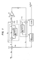
- Fig. 1 is a diagram showing the arrangement of an embodiment of an interpolative D/A converter according to the present invention.
- the difference ⁇ between a digital input signal x composed of a large number of oversampled bits and a digital feedback signal q n is produced by an arithmetic circuit 1-1.
- Such differences ⁇ are integrated by an arithmetic circuit 1-2.
- the output integral signal ⁇ of the circuit 1-2 and the aforementioned difference ⁇ are added by an arithmetic circuit 1-3.
- the added output signal ⁇ + ⁇ is quantized by a comparator 3, and the resulting. signal is applied to an arithmetic circuit 1-4 and is integrated therein.
- the feedback signal q is converted into an analog signal by a D/A converter 4.
- the analog signal being the output of the D/A converter is applied to a filter circuit 3, and the higher harmonics components thereof due to the sampling are removed by the filter.
- Symbols 2-1 and 2-2 denote registers.
- the feature of the embodiment is that the output of the arithmetic circuit or integrator circuit 1-2 is quantized by the comparator 3. Quantization levels in this case is smaller in number than those of the input x n , and at least two quantization levels are included in either minus or plus direction.
- the input signal x n be a digital signal the sampling frequency of which is 512 kHz and one sample of which consists of 16 bits and that the feedback signal q n be a digital signal of 9 bits.
- Fig. 2 shows the practicable arrangement of the interpolative D/A converter in Fig. 1, in which a single adder 1 is used in time-sharing fashion as adders constituting the arithmetic circuits 1-1 to 1-4 in Fig. 1.
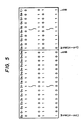
- the timing chart of timing signals ⁇ 1 - ⁇ 4 and ⁇ 1 , ⁇ 2 for use in the embodiment of Fig. 2 is shown in Fig. 3.
- the signals ⁇ 1 - ⁇ 4 are obtained by dividing clock pulses of 512 kHz in four, and those ⁇ 1 and ⁇ 2 are clock pulses of 512 kHz not overlapping each other.
- each of selectors 6-1 to 6-3 is constructed of 16 bits, and it is so operated that when the timing signal applied to a terminal S is logic level "1", an input to a terminal B is selected and is delivered to a terminal Y, whereas when the timing signal is logic level "0", an input to a terminal A is selected and is delivered to the terminal Y.
- each of the register 2-1 and a register 2-3 is constructed of 16 bits, and the register 2-2 is constructed of 9 bits. These registers all have their outputs changed by the trailing edges of the clock pulses ⁇ 1 - ⁇ 4 and hold the output statuses. While the registers 2-1 and 2-2 correspond to those in Fig. 1, the register 2-3 serves for making it possible to use the adder 1 in time-sharing fashion.
- the difference ⁇ (x n - q ) between the input sampled signal x and the feedback signal q n obtained by calculations up to the last-sampled signal x n-1 is produced. More specifically, the input sampled signal x n is applied to the terminal A of the adder 1 via the selectors 6-1 and 6-2 at the timing ⁇ 1 , while the feedback signal q n is applied to the terminal B of the adder 1 via the selector 6-3 at the timing ⁇ 1 .
- the selectors 6-2 and 6-3 select the inputs of their terminals A. Therefore, the terminal A of the adder 1 is supplied with the output of the register 2-3, and the terminal B thereof is supplied with the output of the register 2-1, namely, the integral value of the differences ⁇ up to the last-sampled input x n-1 (execution of the function of the adder 1-3 in Fig. 1).
- the added value ⁇ + ⁇ thus obtained is stored in the register 2-1 again.
- the integral of the differences up to the input sample x n has been performed.
- the selectors 6-2 and 6-3 select the inputs of their terminals A. Therefore, the contents of the registers 2-3 and 2-1 are added, and the result is stored in the register 2-3 again.
- the sum ⁇ + ⁇ between the integral signal ⁇ corresponding to the input x and the difference signal ⁇ is stored in the register 2-3.
- the use of the value ( ⁇ + ⁇ ) for updating the feedback signal q is intended to attain the effect of estimating a feedback signal q n+1 which corresponds to an input signal x n+1 to be subsequently sampled.
- the follow-up property of the feedback signal q n to the input signal x n can be enhanced, and the gradient overload can be effectively suppressed.
- the value of the register 2-3 is decided by the comparator 3 as shown in Fig. 4, and a coefficient for updating the feedback signal q n is output therefrom.
- Fig. 4 shows an example of arrangement of the comparator 3.
- the input ( ⁇ + ⁇ ) is a signal of 16 bits
- the least bits D 9 - D 15 are discarded because the comparison operation is, in other words, a quantization operation.
- a plus value which is at least 0 and less than 1 becomes 0, and a plus value which is at least 1 and less than 2 becomes 1.
- minus values are respectively rounded in the directions of increasing absolute values.
- all the bits D 0 - D 8 are inverted in order to simplify the calculation of the difference ⁇ as stated before, and a carry C i is put into 1 when ( ⁇ + ⁇ ) is minus.
- the carry C i is employed as the carry signal of the ninth bit of the full adder. Owing to this operation, 0, 1, 2, 3, ... become -1, -2, -3, ..., and -1, -2, -3, ... become 1, 2, 3, 4, ..., respectively.
- the output of the comparator 3 is such that the absolute value of ( ⁇ + ⁇ ) is taken and is rounded up, whereupon the sign is inverted.
- the selector 6-1 selects the input of the terminal A
- the selectors 6-2 and 6-3 select the inputs of the terminals B. Therefore, the adder 1 adds the output of the comparator 3 and the content of the register 2-2 and stores the sum in the register 2-2 again. Owing to this operation, the integral calculation of the arithmetic circuit 1-4 in Fig. 1 has been executed.
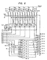
- Fig. 6 shows an example of arrangement of the D/A converter 4 illustrated in Figs. 1 and 2.
- the signal in the two's complement format is converted into a signal having a sign and an absolute value.
- the operation of adding 1 for the minus sum is replaced here with a measure in which a plus offset voltage corresponding to 1 2 LSB is applied to the D/A converter for the plus sum and a minus offset voltage corresponding to 1 2 LSB is applied thereto for the minus sum as will be described later.
- the D/A converter of the present embodiment is constructed of the charge redistribution type which employs the combination of capacitors and resistors (C-arrays 11-1 to 11-6) and (R-strings 12-1, ..., 12-9).
- the capacitances of the C-arrays correspond to the upper 5 bits Q 1 - Q 5 of the input signal bits Q n (n - 1 - 8) and are respectively weighted by the powers of 2 (1, 2, 4, 8, 16).
- the R-strings are divided in eight in correspondence with the lower 3 bits Q 6 - Q 8 , and tap voltages are selected by analog switches 13-1, ... and 13-9 and are connected tothe C-arrays through unit capacitances separately provided.
- resistances of 2 are inserted between the ground and a reference voltage V ref , whereby the aforementioned offset-voltages can be superposed.
- the operation of the D/A converter will be explained concerning a case where a sign signal is plus.
- the upper and lower electrodes of all the C-arrays are simultaneously grounded through switches 15-1, 15-3, 15-5, ... and 15-13 by selectors 14-1 and 14-2, to discharge charges in all the capacitors C.
- the upper electrodes of the capacitors are rendered free potentials at the timing ⁇ 4
- the lower electrodes of the capacitors corresponding to the bits becoming "1" among the bits Q 1 - Q 5 are rendered the reference voltage V ref through the selector 14-2 through gates 10-1, ...
- the plus and minus D/A conversions can be performed with only one reference voltage.
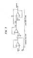
- the output signal of the D/A conversion is delivered as a D/A conversion waveform smoothed through a sample-and-hold circuit and a filter circuit which are exemplified in Fig. 7.
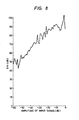
- Fig. 8 Shown in Fig. 8 is the signal (1 kHz)-to-noise (0 - 4 kHz) power ratio characteristic of an interpolative D/A converter fabricated in conformity with the system and arrangement according to the present invention thus far described.
- a favorable D/A conversion characteristic is attained even when signals are sampled at a frequency of or below ⁇ of that in the prior art. Therefore, the characteristics of analog circuit elements can be sharply mitigated.
- a D/A converter circuit which can be integrated on an identical chip with a logic LSI for digital signal processing, or the like can be realized with ease.
Landscapes
- Engineering & Computer Science (AREA)
- Theoretical Computer Science (AREA)
- Analogue/Digital Conversion (AREA)
- Compression, Expansion, Code Conversion, And Decoders (AREA)
Applications Claiming Priority (2)
| Application Number | Priority Date | Filing Date | Title |
|---|---|---|---|
| JP60080131A JPH0697743B2 (ja) | 1985-04-17 | 1985-04-17 | オ−バサンプル形d/a変換器 |
| JP80131/85 | 1985-04-17 |
Publications (3)
| Publication Number | Publication Date |
|---|---|
| EP0199282A2 true EP0199282A2 (fr) | 1986-10-29 |
| EP0199282A3 EP0199282A3 (en) | 1989-04-26 |
| EP0199282B1 EP0199282B1 (fr) | 1992-07-01 |
Family
ID=13709674
Family Applications (1)
| Application Number | Title | Priority Date | Filing Date |
|---|---|---|---|
| EP86105283A Expired EP0199282B1 (fr) | 1985-04-17 | 1986-04-16 | Convertisseur numérique-analogique interpolatif |
Country Status (4)
| Country | Link |
|---|---|
| US (1) | US4652858A (fr) |
| EP (1) | EP0199282B1 (fr) |
| JP (1) | JPH0697743B2 (fr) |
| DE (1) | DE3685836T2 (fr) |
Families Citing this family (13)
| Publication number | Priority date | Publication date | Assignee | Title |
|---|---|---|---|---|
| JPH01112822A (ja) * | 1987-10-26 | 1989-05-01 | Nippon Telegr & Teleph Corp <Ntt> | ノイズシェーピング形d/a変換器 |
| GB8803627D0 (en) * | 1988-02-17 | 1988-03-16 | Data Conversion Systems Ltd | Digital to analogue converter |
| JPH07105724B2 (ja) * | 1989-07-14 | 1995-11-13 | ヤマハ株式会社 | ディジタル・アナログ変換回路 |
| US5854813A (en) * | 1994-12-29 | 1998-12-29 | Motorola, Inc. | Multiple access up converter/modulator and method |
| US5602874A (en) * | 1994-12-29 | 1997-02-11 | Motorola, Inc. | Method and apparatus for reducing quantization noise |
| US5754597A (en) * | 1994-12-29 | 1998-05-19 | Motorola, Inc. | Method and apparatus for routing a digitized RF signal to a plurality of paths |
| US5748683A (en) * | 1994-12-29 | 1998-05-05 | Motorola, Inc. | Multi-channel transceiver having an adaptive antenna array and method |
| US5579341A (en) * | 1994-12-29 | 1996-11-26 | Motorola, Inc. | Multi-channel digital transceiver and method |
| US5668836A (en) * | 1994-12-29 | 1997-09-16 | Motorola, Inc. | Split frequency band signal digitizer and method |
| DE19581533C2 (de) * | 1994-12-29 | 1999-02-25 | Motorola Inc | Verfahren zum Digitalisieren eines Breitbandfrequenzsignals und zugehöriger Breitbandfrequenzsignaldigitalisierer |
| US5710763A (en) * | 1995-07-31 | 1998-01-20 | Motorola, Inc. | Filtered fast Fourier transmultiplexer and method |
| DE19741356C2 (de) * | 1997-09-19 | 2001-02-15 | Cognis Deutschland Gmbh | Verwendung von Glucoprotaminen |
| TW527782B (en) * | 2002-05-22 | 2003-04-11 | Ind Tech Res Inst | Improved capacitor selection method |
Family Cites Families (5)
| Publication number | Priority date | Publication date | Assignee | Title |
|---|---|---|---|---|
| US4109110A (en) * | 1975-02-20 | 1978-08-22 | International Standard Electric Corporation | Digital-to-analog converter |
| GB1580447A (en) * | 1976-12-01 | 1980-12-03 | Post Office | Code converters |
| FR2462062A1 (fr) * | 1979-07-20 | 1981-02-06 | Petit Jean P | Codeur delta sigma a double integration analogique et codeur delta sigma a double integration numerique |
| US4528551A (en) * | 1979-11-28 | 1985-07-09 | International Telephone And Telegraph Corporation | Digital to analog converter employing sigma-delta modulation for use in telephone systems |
| DE3021012C2 (de) * | 1980-06-03 | 1985-08-22 | ANT Nachrichtentechnik GmbH, 7150 Backnang | Verallgemeinertes interpolativers Verfahren zur Digital-Analog-Umsetzung von PCM Signalen |
-
1985
- 1985-04-17 JP JP60080131A patent/JPH0697743B2/ja not_active Expired - Lifetime
-
1986
- 1986-04-16 EP EP86105283A patent/EP0199282B1/fr not_active Expired
- 1986-04-16 US US06/852,749 patent/US4652858A/en not_active Expired - Lifetime
- 1986-04-16 DE DE8686105283T patent/DE3685836T2/de not_active Expired - Fee Related
Also Published As
| Publication number | Publication date |
|---|---|
| DE3685836T2 (de) | 1993-02-04 |
| EP0199282B1 (fr) | 1992-07-01 |
| DE3685836D1 (de) | 1992-08-06 |
| JPS61239723A (ja) | 1986-10-25 |
| US4652858A (en) | 1987-03-24 |
| EP0199282A3 (en) | 1989-04-26 |
| JPH0697743B2 (ja) | 1994-11-30 |
Similar Documents
| Publication | Publication Date | Title |
|---|---|---|
| US5221926A (en) | Circuit and method for cancelling nonlinearity error associated with component value mismatches in a data converter | |
| US4890106A (en) | Apparatus and methods for digital-to-analog conversion using modified LSB switching | |
| EP0368610B1 (fr) | Méthode pour mettre en cascade plusieurs modulateurs sigma delta et un système modulateur sigma delta | |
| US4652858A (en) | Interpolative D/A converter | |
| US4450433A (en) | D/A Converting circuit having two D/A converters for decoding and converting a digital signal into an analog signal | |
| EP0227871B1 (fr) | Convertisseur numérique-analogique parallèle algorithmique | |
| EP0021650A1 (fr) | Convertisseur analogique-numérique | |
| US6100834A (en) | Recursive multi-bit ADC with predictor | |
| US4663610A (en) | Serial digital-to-analog converter | |
| US5134402A (en) | Tri-level digital-analog converter and analog-digital converter having tri-level digital-analog converter | |
| CN1203484A (zh) | 具有较高线性的数-模转换器件 | |
| JPH0783267B2 (ja) | 2進信号をこれに比例する直流信号に変換する装置 | |
| US5812831A (en) | Method and apparatus for pulse width modulation | |
| US5084701A (en) | Digital-to-analog converter using cyclical current source switching | |
| CA2039697C (fr) | Convertisseur numerique-analogique | |
| JP3956582B2 (ja) | A/d変換回路 | |
| EP0251758A2 (fr) | Système de conversion numérique-analogique | |
| KR950003287B1 (ko) | 디지탈 투 아날로그 컨버터내의 양극성 영점에서 주요 비트 전송에러를 제거하는 회로 및 방법 | |
| US4924223A (en) | Digital code converter formed of a decreased number of circuit elements | |
| JPS6222289B2 (fr) | ||
| US5699064A (en) | Oversampling D/A converter using a bidirectional shift register | |
| JP3142747B2 (ja) | オーバーサンプリングda変換器 | |
| US4791405A (en) | Data converter for directly providing outputs in two's complement code | |
| JP2001077692A (ja) | D/a変換回路 | |
| USRE34660E (en) | Apparatus and methods for digital-to-analog conversion using modified LSB switching |
Legal Events
| Date | Code | Title | Description |
|---|---|---|---|
| PUAI | Public reference made under article 153(3) epc to a published international application that has entered the european phase |
Free format text: ORIGINAL CODE: 0009012 |
|
| AK | Designated contracting states |
Kind code of ref document: A2 Designated state(s): DE FR GB IT |
|
| PUAL | Search report despatched |
Free format text: ORIGINAL CODE: 0009013 |
|
| AK | Designated contracting states |
Kind code of ref document: A3 Designated state(s): DE FR GB IT |
|
| 17P | Request for examination filed |
Effective date: 19890929 |
|
| 17Q | First examination report despatched |
Effective date: 19900809 |
|
| GRAA | (expected) grant |
Free format text: ORIGINAL CODE: 0009210 |
|
| AK | Designated contracting states |
Kind code of ref document: B1 Designated state(s): DE FR GB IT |
|
| REF | Corresponds to: |
Ref document number: 3685836 Country of ref document: DE Date of ref document: 19920806 |
|
| ITF | It: translation for a ep patent filed | ||
| ET | Fr: translation filed | ||
| PLBE | No opposition filed within time limit |
Free format text: ORIGINAL CODE: 0009261 |
|
| STAA | Information on the status of an ep patent application or granted ep patent |
Free format text: STATUS: NO OPPOSITION FILED WITHIN TIME LIMIT |
|
| 26N | No opposition filed | ||
| PGFP | Annual fee paid to national office [announced via postgrant information from national office to epo] |
Ref country code: FR Payment date: 19970418 Year of fee payment: 12 |
|
| PGFP | Annual fee paid to national office [announced via postgrant information from national office to epo] |
Ref country code: DE Payment date: 19970626 Year of fee payment: 12 |
|
| PG25 | Lapsed in a contracting state [announced via postgrant information from national office to epo] |
Ref country code: FR Free format text: THE PATENT HAS BEEN ANNULLED BY A DECISION OF A NATIONAL AUTHORITY Effective date: 19980430 |
|
| PG25 | Lapsed in a contracting state [announced via postgrant information from national office to epo] |
Ref country code: DE Free format text: LAPSE BECAUSE OF NON-PAYMENT OF DUE FEES Effective date: 19990202 |
|
| REG | Reference to a national code |
Ref country code: FR Ref legal event code: ST |
|
| PGFP | Annual fee paid to national office [announced via postgrant information from national office to epo] |
Ref country code: GB Payment date: 19990325 Year of fee payment: 14 |
|
| PG25 | Lapsed in a contracting state [announced via postgrant information from national office to epo] |
Ref country code: GB Free format text: LAPSE BECAUSE OF NON-PAYMENT OF DUE FEES Effective date: 20000416 |
|
| GBPC | Gb: european patent ceased through non-payment of renewal fee |
Effective date: 20000416 |
|
| PG25 | Lapsed in a contracting state [announced via postgrant information from national office to epo] |
Ref country code: IT Free format text: LAPSE BECAUSE OF NON-PAYMENT OF DUE FEES;WARNING: LAPSES OF ITALIAN PATENTS WITH EFFECTIVE DATE BEFORE 2007 MAY HAVE OCCURRED AT ANY TIME BEFORE 2007. THE CORRECT EFFECTIVE DATE MAY BE DIFFERENT FROM THE ONE RECORDED. Effective date: 20050416 |