EP0199565B1 - Dispositif laser à semi-conducteur pour tête optique - Google Patents
Dispositif laser à semi-conducteur pour tête optique Download PDFInfo
- Publication number
- EP0199565B1 EP0199565B1 EP86302954A EP86302954A EP0199565B1 EP 0199565 B1 EP0199565 B1 EP 0199565B1 EP 86302954 A EP86302954 A EP 86302954A EP 86302954 A EP86302954 A EP 86302954A EP 0199565 B1 EP0199565 B1 EP 0199565B1
- Authority
- EP
- European Patent Office
- Prior art keywords
- semiconductor laser
- photodetector
- beam splitter
- laser chip
- laser apparatus
- Prior art date
- Legal status (The legal status is an assumption and is not a legal conclusion. Google has not performed a legal analysis and makes no representation as to the accuracy of the status listed.)
- Expired - Lifetime
Links
Images


Classifications
-
- H—ELECTRICITY
- H01—ELECTRIC ELEMENTS
- H01S—DEVICES USING THE PROCESS OF LIGHT AMPLIFICATION BY STIMULATED EMISSION OF RADIATION [LASER] TO AMPLIFY OR GENERATE LIGHT; DEVICES USING STIMULATED EMISSION OF ELECTROMAGNETIC RADIATION IN WAVE RANGES OTHER THAN OPTICAL
- H01S5/00—Semiconductor lasers
- H01S5/02—Structural details or components not essential to laser action
- H01S5/022—Mountings; Housings
- H01S5/02208—Mountings; Housings characterised by the shape of the housings
- H01S5/02212—Can-type, e.g. TO-CAN housings with emission along or parallel to symmetry axis
-
- G—PHYSICS
- G11—INFORMATION STORAGE
- G11B—INFORMATION STORAGE BASED ON RELATIVE MOVEMENT BETWEEN RECORD CARRIER AND TRANSDUCER
- G11B7/00—Recording or reproducing by optical means, e.g. recording using a thermal beam of optical radiation by modifying optical properties or the physical structure, reproducing using an optical beam at lower power by sensing optical properties; Record carriers therefor
- G11B7/08—Disposition or mounting of heads or light sources relatively to record carriers
- G11B7/09—Disposition or mounting of heads or light sources relatively to record carriers with provision for moving the light beam or focus plane for the purpose of maintaining alignment of the light beam relative to the record carrier during transducing operation, e.g. to compensate for surface irregularities of the latter or for track following
- G11B7/0908—Disposition or mounting of heads or light sources relatively to record carriers with provision for moving the light beam or focus plane for the purpose of maintaining alignment of the light beam relative to the record carrier during transducing operation, e.g. to compensate for surface irregularities of the latter or for track following for focusing only
- G11B7/0909—Disposition or mounting of heads or light sources relatively to record carriers with provision for moving the light beam or focus plane for the purpose of maintaining alignment of the light beam relative to the record carrier during transducing operation, e.g. to compensate for surface irregularities of the latter or for track following for focusing only by astigmatic methods
-
- G—PHYSICS
- G11—INFORMATION STORAGE
- G11B—INFORMATION STORAGE BASED ON RELATIVE MOVEMENT BETWEEN RECORD CARRIER AND TRANSDUCER
- G11B7/00—Recording or reproducing by optical means, e.g. recording using a thermal beam of optical radiation by modifying optical properties or the physical structure, reproducing using an optical beam at lower power by sensing optical properties; Record carriers therefor
- G11B7/12—Heads, e.g. forming of the optical beam spot or modulation of the optical beam
- G11B7/123—Integrated head arrangements, e.g. with source and detectors mounted on the same substrate
-
- H—ELECTRICITY
- H01—ELECTRIC ELEMENTS
- H01S—DEVICES USING THE PROCESS OF LIGHT AMPLIFICATION BY STIMULATED EMISSION OF RADIATION [LASER] TO AMPLIFY OR GENERATE LIGHT; DEVICES USING STIMULATED EMISSION OF ELECTROMAGNETIC RADIATION IN WAVE RANGES OTHER THAN OPTICAL
- H01S5/00—Semiconductor lasers
- H01S5/005—Optical components external to the laser cavity, specially adapted therefor, e.g. for homogenisation or merging of the beams or for manipulating laser pulses, e.g. pulse shaping
-
- H—ELECTRICITY
- H01—ELECTRIC ELEMENTS
- H01S—DEVICES USING THE PROCESS OF LIGHT AMPLIFICATION BY STIMULATED EMISSION OF RADIATION [LASER] TO AMPLIFY OR GENERATE LIGHT; DEVICES USING STIMULATED EMISSION OF ELECTROMAGNETIC RADIATION IN WAVE RANGES OTHER THAN OPTICAL
- H01S5/00—Semiconductor lasers
- H01S5/02—Structural details or components not essential to laser action
- H01S5/022—Mountings; Housings
- H01S5/023—Mount members, e.g. sub-mount members
- H01S5/02325—Mechanically integrated components on mount members or optical micro-benches
-
- H—ELECTRICITY
- H01—ELECTRIC ELEMENTS
- H01S—DEVICES USING THE PROCESS OF LIGHT AMPLIFICATION BY STIMULATED EMISSION OF RADIATION [LASER] TO AMPLIFY OR GENERATE LIGHT; DEVICES USING STIMULATED EMISSION OF ELECTROMAGNETIC RADIATION IN WAVE RANGES OTHER THAN OPTICAL
- H01S5/00—Semiconductor lasers
- H01S5/06—Arrangements for controlling the laser output parameters, e.g. by operating on the active medium
- H01S5/068—Stabilisation of laser output parameters
- H01S5/0683—Stabilisation of laser output parameters by monitoring the optical output parameters
Definitions
- This invention relates to semiconductor laser apparatus for optical heads of optical recording/reproducing apparatus.
- Such semiconductor laser apparatus is used for performing beam irradiation and incident beam detection.
- An optical head used in an optical recording/reproducing apparatus irradiates an optical recording medium with a beam, and detects a modulated beam from the optical recording medium, to perform information recording/reproducing.
- the optical head normally uses a semiconductor laser apparatus.
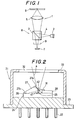
- Figure 1 to which reference is now made shows an optical head 1 using a known semiconductor laser apparatus.
- a beam 4 radiated from a semiconductor laser 2 and reflected by a beam splitter 3 is incident on an optical recording medium 6 through an objective lens 5.
- the beam 4, reflected by the optical recording medium 6 and passing through the objective lens 5 and the beam splitter 3, is incident on a photodetector 7.
- the semiconductor laser 2, the beam splitter 3, and the photodetector 7 form a semiconductor laser apparatus 8.
- the need for positional adjustment of the three separate optical components results in a high cost for the optical head 1.
- the optical head 1 scans the optical recording medium 6 without contact, so focus servo control is required.
- An astigmatism method is normally used to detect focus error.
- a cylindrical lens 9 is usually arranged between the beam splitter 3 and the photodetector 7, the above problem becomes even more severe.
- European patent specification EP-A1-0 029 755 discloses apparatus comprising a semiconductor laser chip for radiating a beam from a radiant surface thereof, a photodetector for detecting an incident beam and supplying a signal, and a beam splitter having a first surface inclined at a predetermined angle with respect to said radiant surface, said beam splitter being fixed on said photodetector.
- European patent specification EP-A1 0 061 384 discloses a semiconductor laser apparatus comprising a semiconductor laser chip for radiating a beam from a radiant surface thereof, a photodetector for detecting an incident beam and supplying a signal, and a beam splitter having a first surface inclined at a predetermined angle with respect to said radiant surface.
- Japanese patent specification JP-A-56 93388 discloses semiconductor laser apparatus similar to the pre-characterizing part of claim 1.
- a semiconductor laser apparatus for an optical head comprising: a semiconductor laser chip for radiating a beam from a radiant surface thereof; a photodetector for detecting an incident beam and supplying a signal; said semiconductor laser chip and said photodetector being arranged on a common substrate; and a beam splitter fixed on said photodetector and having a first surface inclined at a predetermined angle with respect to said radiant surface; characterized in that: there is further provided another photodetector, and said beam splitter has a second surface for directing those rays of the beam radiated from said semiconductor laser chip which are transmitted through said first surface of said beam splitter, towards said other photodetector, so that an output from said semiconductor laser chip is monitored by a signal from said other photodetector.
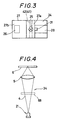
- Figures 2 and 3 show the first embodiment.
- a silicon substrate 24 is fixed on a stem 23 with leads 22.
- a PIN diode 25 used as a signal detecting photodetector and a PIN diode 26 used as a laser output monitoring photodetector are formed on the silicon substrate 24.
- a triangular prism 27 is fixed by an adhesive to the silicon substrate 24 to cover the PIN diodes 25 and 26.
- a silicon substrate 28 integrally formed with the silicon substrate 24 projects next to the triangular prism 27.
- a laser diode chip 31 used as a semiconductor laser is arranged at the edge of the silicon substrate 28 beside the triangular prism 27.
- An inclined surface 27a of the triangular prism 27 opposite the laser diode chip 31 has a reflectivity of about 50%.
- Another inclined surface 27b has a totally reflective coating, that is, a reflectivity of 100%.
- a cap 33 with a window glass 32 is mounted on the stem 23 hermetically to seal the optical sytstem.
- the PIN diodes 25 and 26 and the laser diode chip 31 are connected to the leads 22 by wires (not shown).
- Figure 4 shows an optical head 34 employing the semiconductor laser apparatus 21.
- a beam 4 radiated from the laser diode chip 31 and reflected by the inclined surface 27a of the triangular prism 27 is transmitted through the window glass 32 and an objective lens 5, and is incident on an optical recording medium 6.
- the beam 4 reflected by the optical recording medium 6 and transmitted through the window glass 32 and the inclined surface 27a is incident on the PIN diode 25.
- the beam 4 reflected by the optical recording medium 6 is incident on the inclined surface 27a in a converged state.
- the beam 4 is subjected to astigmatism and is incident on the PIN diode 25.
- a beam spot 35 of the beam incident on the PIN diode 25 in a focused state is of the shape shown in Figure 5B.
- a beam spot 35 having the shape shown in Figure 5A or 5C is then formed on the PIN diode 25 in accordance with its displacement from the focused state.
- the PIN diode 25 comprises four photodetecting portions A to D divided by two bisectors inclined at 45° in opposite directions with respect to the ridge of the triangular prism 27.
- a focus error signal (A + C) - (B + D) can be derived from a subtracter 36 which receives signals from the four photodetecting portions A to D forming the PIN diode 25, and a tracking error signal and a reproduced signal A + B + C + D can be derived from a phase comparator 37 and an adder 38, respectively.
- the beam 4 radiated from the laser diode chip 31 is transmitted through the inclined surface 27a of the triangular prism 27 and is incident on the PIN diode 26 either directly or after being reflected by the inclined surface 27b. Therefore, the output from the laser diode chip 31 can be adjusted on the basis of the output from the PIN diode 26.
- the beam 4 radiated from the laser diode chip 31 and reflected by the inclined surface 27a of the triangular prism 27 does not directly return to the laser diode chip 31. For this reason, little noise is generated by the laser diode chip 31.
- the semiconductor laser apparatus 21 is inexpensive.
- the PIN diodes 25 and 26 are formed on the same surface of the single silicon substrate 24, the PIN diodes 25 and 26 can be simultaneously formed by a lithographic technique.
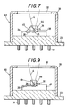
- FIG. 7 shows the second embodiment.
- a semiconductor laser apparatus 43 of the second embodiment is substantially the same as that of the first embodiment ( Figure 2), except that a beam splitter is formed by two rectangular prisms 44 and 45 having different refractive indices.
- Figure 8 shows levels of signals from the PIN diode 25 when the semiconductor laser apparatus 43 of the second embodiment is used in an optical head upon displacement of an optical recording medium 6 along the optical axis of a beam 4.
- the rectangular prisms 44 and 45 forming a 1 mm high beam splitter are of optical glass BK7 and SF11, the NA of the objective lens 5 is 0.47, and the NA of a collimator lens (not shown in Figure 4) is 0.14.
- FIG. 9 shows the third embodiment.
- a semiconductor laser apparatus 46 of the third embodiment is substantially the same as that of the first embodiment ( Figure 2), except that PIN diodes 25 and 26 and a laser diode chip 31 are formed on an integral silicon substrate 47, and a beam splitter formed by two rectangular prisms 48 and 49 having refractive indices different from each other is fixed on the silicon substrate 47 at a position above only a PIN diode 25.
- FIG. 10 shows the fourth embodiment.
- a semiconductor laser apparatus 51 of the fourth embodiment is substantially the same as that of the third embodiment ( Figure 9), except that a silicon substrate 28 is integrally formed with a silicon substrate 24, and a laser output monitoring PIN diode 26 is formed in the silicon substrate 28 having a laser diode chip 31 thereon.
- the PIN diode 26 serves as a back monitor element of the laser diode chip 31.
- FIG. 11 shows the fifth embodiment.
- a semiconductor laser apparatus 52 of the fifth embodiment is substantially the same as that of the fourth embodiment ( Figure 10), except that a PIN diode 26 is formed on a silicon substrate 24 having a PIN diode 25 thereon.
Landscapes
- Physics & Mathematics (AREA)
- Optics & Photonics (AREA)
- Condensed Matter Physics & Semiconductors (AREA)
- General Physics & Mathematics (AREA)
- Electromagnetism (AREA)
- Optical Head (AREA)
- Semiconductor Lasers (AREA)
- Laser Beam Processing (AREA)
Claims (5)
- Dispositif laser à semi-conducteur (21) pour tête optique, le dispositif (21) comprenant :
un circuit intégré laser à semi-conducteur (31) pour émettre un faisceau à partir d'une surface rayonnante de celui-ci ;
un photodétecteur (25) pour détecter un faisceau incident et délivrer un signal ;
ledit circuit intégré laser à semi-conducteur (31) et ledit photodétecteur (25) étant disposé sur un substrat commun (24, 28) ; et,
un séparateur de faisceau (27) fixé sur ledit photodétecteur (25) et comportant une première surface inclinée (27a) selon un angle prédéterminé par rapport à ladite surface rayonnante ;
caractérisé en ce qu'il est prévu en outre un autre photodétecteur (26), et en ce que ledit séparateur de faisceau (27) possède une seconde surface (27b) pour diriger ceux des rayons du faisceau émis par ledit circuit intégré laser à semi-conducteur (31) qui sont transmis à travers ladite première surface (27a) dudit séparateur de faisceau (27), en direction dudit autre photodétecteur (26), de manière à ce que la sortie dudit circuit intégré laser à semi-conducteur (31) soit pilotée par un signal issu dudit autre photodétecteur (26). - Dispositif (21) selon la revendication 1 comprenant de plus une fenêtre (32) pour recevoir un faisceau émis à partir dudit circuit intégré laser à semi-conducteur (31) et réfléchi par ladite première surface (27a) dudit séparateur de faisceau (27), et pour recevoir le faisceau réfléchi par un support d'enregistrement optique (6).
- Dispositif (21) selon la revendication 2, dans lequel ledit séparateur de faisceau (27) comprend un prisme (27), et ledit photodétecteur (25) comprend quatre parties photodétectrices (A, B, C, D) divisées par deux bissectrices inclinées à 45° dans des directions opposées à l'arrête dudit séparateur de faisceau (27), deux paires desdites parties photodétectrices (A, B, C, D), disposées de manière symétrique par rapport à l'intersection des deux bissectrices étant agencées pour produire des sorties pour obtenir un signal d'erreur de focalisation, le signal d'erreur de focalisation étant calculé comme un astigmatisme à partir de la différence entre la somme des sorties de l'une des paires de parties photodétectrices opposées (A, B, C, D) et la somme des sorties de l'autre paire de parties photodétectrices opposées (A, B, C, D).
- Dispositif (21) selon la revendication 3, dans lequel la somme totale des sorties desdites parties photodétectrices (A, B, C, D) forme un signal reproduit.
- Dispositif (21) selon la revendication 3, dans lequel ledit prisme (27) comprend un premier et un second prismes triangulaires (44, 45) ayant des indices de réfraction différents l'un de l'autre.
Priority Applications (1)
| Application Number | Priority Date | Filing Date | Title |
|---|---|---|---|
| AT86302954T ATE82438T1 (de) | 1985-04-22 | 1986-04-18 | Halbleiterlaservorrichtung fuer optischen kopf. |
Applications Claiming Priority (4)
| Application Number | Priority Date | Filing Date | Title |
|---|---|---|---|
| JP86179/85 | 1985-04-22 | ||
| JP60086178A JPS61243963A (ja) | 1985-04-22 | 1985-04-22 | 半導体レ−ザ装置 |
| JP86178/85 | 1985-04-22 | ||
| JP60086179A JP2609221B2 (ja) | 1985-04-22 | 1985-04-22 | 半導体レーザ装置 |
Publications (3)
| Publication Number | Publication Date |
|---|---|
| EP0199565A2 EP0199565A2 (fr) | 1986-10-29 |
| EP0199565A3 EP0199565A3 (en) | 1988-01-20 |
| EP0199565B1 true EP0199565B1 (fr) | 1992-11-11 |
Family
ID=26427341
Family Applications (1)
| Application Number | Title | Priority Date | Filing Date |
|---|---|---|---|
| EP86302954A Expired - Lifetime EP0199565B1 (fr) | 1985-04-22 | 1986-04-18 | Dispositif laser à semi-conducteur pour tête optique |
Country Status (6)
| Country | Link |
|---|---|
| US (1) | US4733067A (fr) |
| EP (1) | EP0199565B1 (fr) |
| AT (1) | ATE82438T1 (fr) |
| AU (1) | AU584188B2 (fr) |
| CA (1) | CA1258906A (fr) |
| DE (1) | DE3687078T2 (fr) |
Families Citing this family (67)
| Publication number | Priority date | Publication date | Assignee | Title |
|---|---|---|---|---|
| US6657931B1 (en) * | 1959-02-02 | 2003-12-02 | Sony Corporation | Optical disc drive for performing read/write operations on optical disks |
| JP2615553B2 (ja) * | 1985-11-14 | 1997-05-28 | 富士通株式会社 | レーザ制御装置 |
| WO1987005142A1 (fr) * | 1986-02-24 | 1987-08-27 | Sony Corporation | Dispositif de detection de foyer |
| US4906839A (en) * | 1986-05-01 | 1990-03-06 | Pencom International Corp. | Hybrid surface emitting laser and detector |
| US4905216A (en) * | 1986-12-04 | 1990-02-27 | Pencom International Corporation | Method for constructing an optical head by varying a hologram pattern |
| JP2508478B2 (ja) * | 1987-02-06 | 1996-06-19 | ソニー株式会社 | 光学ヘツド |
| GB8712808D0 (en) * | 1987-06-01 | 1987-07-08 | Bt & D Technologies Ltd | Optical transmitters |
| JP2590902B2 (ja) * | 1987-07-30 | 1997-03-19 | ソニー株式会社 | 発光・受光複合素子 |
| EP0305169B1 (fr) * | 1987-08-24 | 1994-05-11 | Sharp Kabushiki Kaisha | Appareil de lecture optique et assemblage des réseaux de diffraction à cet effet |
| EP0308749A3 (fr) * | 1987-09-25 | 1990-07-11 | Siemens Aktiengesellschaft | Groupe électro-optique |
| AU620581B2 (en) * | 1987-12-03 | 1992-02-20 | Bt&D Technologies Limited | Light sources |
| GB8728342D0 (en) * | 1987-12-03 | 1988-01-06 | Bt & D Technologies Ltd | Light sources |
| EP0339722B1 (fr) * | 1988-04-26 | 1993-10-06 | Koninklijke Philips Electronics N.V. | Dispositif pour explorer un support d'enregistrement magnéto-optique |
| US4854659A (en) * | 1988-05-31 | 1989-08-08 | Bt&D Technologies, Ltd. | Optical devices |
| EP0360209A3 (fr) * | 1988-09-19 | 1992-08-19 | Hitachi, Ltd. | Tête optique et appareil optique pour le traitement de données |
| NL8802988A (nl) * | 1988-12-05 | 1990-07-02 | Philips Nv | Inrichting voor het met optische straling aftasten van een informatievlak. |
| JPH0724112B2 (ja) * | 1988-12-19 | 1995-03-15 | ローム株式会社 | レーザダイオードユニットの取り付け方法 |
| US5233580A (en) * | 1988-12-19 | 1993-08-03 | Rohm Co., Ltd. | Laser diode unit welded to a mounting member by laser light |
| US5130531A (en) * | 1989-06-09 | 1992-07-14 | Omron Corporation | Reflective photosensor and semiconductor light emitting apparatus each using micro Fresnel lens |
| US5226052A (en) * | 1990-05-08 | 1993-07-06 | Rohm, Ltd. | Laser diode system for cutting off the environment from the laser diode |
| US5089861A (en) * | 1990-05-09 | 1992-02-18 | Rohm Co., Ltd. | Semiconductor laser device with mounting block |
| US5625483A (en) * | 1990-05-29 | 1997-04-29 | Symbol Technologies, Inc. | Integrated light source and scanning element implemented on a semiconductor or electro-optical substrate |
| US5966230A (en) * | 1990-05-29 | 1999-10-12 | Symbol Technologies, Inc. | Integrated scanner on a common substrate |
| US6305607B1 (en) * | 1990-05-29 | 2001-10-23 | Symbol Technologies, Inc. | Integrated bar code reader and RF transceiver |
| US5164930A (en) * | 1990-07-25 | 1992-11-17 | Pioneer Electronic Corporation | Optical pickup |
| US5191204A (en) * | 1991-10-28 | 1993-03-02 | International Business Machines Corporation | Multi-beam optical system and method with power detection of overlapping beams |
| US5319182A (en) * | 1992-03-04 | 1994-06-07 | Welch Allyn, Inc. | Integrated solid state light emitting and detecting array and apparatus employing said array |
| US5247167A (en) * | 1992-08-06 | 1993-09-21 | International Business Machines Corporation | Multiple beam power monitoring system and method with radiation detection and focusing means of overlapping beams |
| DE69318487T2 (de) * | 1992-08-07 | 1998-12-24 | Matsushita Electric Industrial Co., Ltd., Kadoma, Osaka | Halbleiterlaservorrichtung, optische Vorrichtung und Herstellungsverfahren |
| US5581523A (en) * | 1992-11-17 | 1996-12-03 | Seiko Epson Corporation | Laser emission unit, optical head and optical memory device |
| JPH06169136A (ja) * | 1992-11-30 | 1994-06-14 | Canon Inc | 発光装置と光半導体装置及びその製造方法 |
| US5557116A (en) * | 1992-12-24 | 1996-09-17 | Sharp Kabushiki Kaisha | Semiconductor laser device and resin layer |
| JPH06309685A (ja) * | 1993-04-26 | 1994-11-04 | Nippon Conlux Co Ltd | 光学式情報記録再生装置のレーザ出力制御装置 |
| US5852287A (en) * | 1993-08-17 | 1998-12-22 | Sony Corporation | Semiconductor optical device for code reader |
| DE69425319T2 (de) * | 1993-08-17 | 2001-01-18 | Sony Corp., Tokio/Tokyo | OPTISCHE VORRICHTUNG FüR KODELESER |
| JPH07114746A (ja) * | 1993-08-25 | 1995-05-02 | Sony Corp | 光学装置 |
| US6648227B2 (en) * | 2000-10-20 | 2003-11-18 | Symbol Technologies, Inc. | Scanning module for a bar code reader with a focusing lens |
| US6114712A (en) * | 1996-10-09 | 2000-09-05 | Symbol Technologies, Inc. | One piece optical assembly for low cost optical scanner |
| EP0660467B1 (fr) * | 1993-12-22 | 1997-03-19 | Siemens Aktiengesellschaft | Elément optoélectronique et sa méthode de fabrication |
| EP0664585B1 (fr) * | 1993-12-22 | 1998-03-04 | Siemens Aktiengesellschaft | Module de transmission et de réception pour système de communication bidirectionnel |
| US5874722A (en) | 1994-07-19 | 1999-02-23 | Spectra-Physics Scanning Systems, Inc. | Compact scanner module mountable to pointing instrument |
| JP3438365B2 (ja) * | 1994-11-29 | 2003-08-18 | ソニー株式会社 | 複合光学装置およびその製造方法 |
| US5787058A (en) * | 1995-05-31 | 1998-07-28 | Daewoo Electronics Co., Ltd. | Optical pickup apparatus utilizing a polygonal prism |
| KR100200857B1 (ko) * | 1995-10-04 | 1999-06-15 | 윤종용 | 광픽업장치 |
| DE19640421A1 (de) * | 1996-09-30 | 1998-04-23 | Siemens Ag | Optoelektronisches Modul zur bidirektionalen optischen Datenübertragung |
| US6097521A (en) * | 1997-09-26 | 2000-08-01 | Siemens Aktiengesellschaft | Optoelectronic module for bidirectional optical data transmission |
| US6236859B1 (en) | 1996-10-23 | 2001-05-22 | Siemens Aktiengesellschaft | Method for the location registration of a mobile terminal |
| US6185239B1 (en) * | 1997-01-22 | 2001-02-06 | Sony Corporation | Semiconductor laser device |
| WO1998050814A1 (fr) * | 1997-05-05 | 1998-11-12 | Roustaei Alexander R | Explorateur optique et lecteur d'images pour la lecture d'images et le decodage d'informations optiques, y compris les symboles en une et deux dimensions a profondeur de champ variable |
| DE19748324C2 (de) * | 1997-10-31 | 1999-08-26 | Siemens Ag | Optoelektronisches Sensormodul |
| US6206290B1 (en) * | 1998-03-06 | 2001-03-27 | Symbol Technologies, Inc. | Control system for oscillating optical element in scanners |
| US6186400B1 (en) * | 1998-03-20 | 2001-02-13 | Symbol Technologies, Inc. | Bar code reader with an integrated scanning component module mountable on printed circuit board |
| US6843416B2 (en) * | 2002-01-29 | 2005-01-18 | Symbol Technologies, Inc. | Integrated scanner on a common substrate |
| US6807218B1 (en) | 2002-05-13 | 2004-10-19 | Amkor Technology, Inc. | Laser module and optical subassembly |
| JP2003332671A (ja) * | 2002-05-17 | 2003-11-21 | Sharp Corp | 半導体レーザ装置および光ピックアップ装置 |
| JP2004152845A (ja) * | 2002-10-29 | 2004-05-27 | Sharp Corp | 半導体レーザ装置 |
| JP2004311860A (ja) * | 2003-04-10 | 2004-11-04 | Sony Corp | 光集積型装置 |
| US7225987B2 (en) * | 2003-09-11 | 2007-06-05 | Symbol Technologies, Inc. | Integrated scanner on a common substrate |
| US7449667B2 (en) * | 2005-12-19 | 2008-11-11 | Motorola, Inc. | Illumination method and apparatus having a plurality of feedback control circuit for controlling intensities of multiple light sources |
| US7405384B2 (en) * | 2005-12-19 | 2008-07-29 | Motorola, Inc. | Method and apparatus for intensity control of multiple light sources using source timing |
| WO2008038924A1 (fr) | 2006-09-28 | 2008-04-03 | Seoul Opto Device Co., Ltd. | Ensemble diode électroluminescente ultraviolette |
| US8235605B2 (en) * | 2007-03-19 | 2012-08-07 | Jeong Soo Kim | Self-standing parallel plate beam splitter, method for manufacturing the same, and laser diode package structure using the same |
| KR102217730B1 (ko) * | 2013-07-30 | 2021-02-22 | 주식회사 포벨 | 파장 측정 장치가 내장된 외부 공진기형 레이저 |
| WO2016154261A1 (fr) * | 2015-03-24 | 2016-09-29 | Samtec, Inc. | Bloc optique avec surface texturée |
| JP6217706B2 (ja) * | 2015-07-29 | 2017-10-25 | 日亜化学工業株式会社 | 光学部材の製造方法、半導体レーザ装置の製造方法及び半導体レーザ装置 |
| US20220166185A1 (en) * | 2019-08-06 | 2022-05-26 | Mitsubishi Electric Corporation | Semiconductor laser device |
| TWI864942B (zh) * | 2022-08-05 | 2024-12-01 | 華信光電科技股份有限公司 | 電子元件封裝體及其製造方法 |
Family Cites Families (11)
| Publication number | Priority date | Publication date | Assignee | Title |
|---|---|---|---|---|
| NL7312139A (fr) * | 1972-09-08 | 1974-03-12 | ||
| DE2737345C2 (de) * | 1976-08-20 | 1991-07-25 | Canon K.K., Tokio/Tokyo | Halbleiterlaser-Vorrichtung mit einem Peltier-Element |
| CA1091966A (fr) * | 1976-10-15 | 1980-12-23 | Chiaki Kojima | Appareil de lecture de signaux enregistres sur support |
| US4293826A (en) * | 1979-04-30 | 1981-10-06 | Xerox Corporation | Hybrid semiconductor laser/detectors |
| FR2470391A1 (fr) * | 1979-11-21 | 1981-05-29 | Thomson Csf | Dispositif optique stigmatique d'emission-reception de rayonnements coherents et tete optique d'enregistrement-lecture comprenant un tel dispositif |
| US4284884A (en) * | 1980-04-09 | 1981-08-18 | Northern Telecom Limited | Electro-optic devices |
| FR2502800A1 (fr) * | 1981-03-24 | 1982-10-01 | Thomson Csf | Senseur optique d'asservissement de focalisation |
| JPS5880139A (ja) * | 1981-11-04 | 1983-05-14 | Sony Corp | 光学ヘツド |
| JPS58155527A (ja) * | 1982-03-10 | 1983-09-16 | Hitachi Ltd | 光デイスクプレ−ヤのフオ−カス引き込み回路 |
| US4626679A (en) * | 1982-09-22 | 1986-12-02 | Canon Kabushiki Kaisha | Optical head and method of detecting the focus thereof |
| NL8502802A (nl) * | 1985-10-14 | 1987-05-04 | Philips Nv | Inrichting voor het uitlezen en/of inschrijven van een optische spoorvormige informatiestruktuur. |
-
1986
- 1986-04-14 CA CA000506609A patent/CA1258906A/fr not_active Expired
- 1986-04-17 US US06/853,210 patent/US4733067A/en not_active Expired - Lifetime
- 1986-04-18 EP EP86302954A patent/EP0199565B1/fr not_active Expired - Lifetime
- 1986-04-18 DE DE8686302954T patent/DE3687078T2/de not_active Expired - Fee Related
- 1986-04-18 AT AT86302954T patent/ATE82438T1/de not_active IP Right Cessation
- 1986-04-21 AU AU56427/86A patent/AU584188B2/en not_active Ceased
Also Published As
| Publication number | Publication date |
|---|---|
| AU584188B2 (en) | 1989-05-18 |
| CA1258906A (fr) | 1989-08-29 |
| DE3687078D1 (de) | 1992-12-17 |
| EP0199565A3 (en) | 1988-01-20 |
| AU5642786A (en) | 1986-10-30 |
| ATE82438T1 (de) | 1992-11-15 |
| US4733067A (en) | 1988-03-22 |
| EP0199565A2 (fr) | 1986-10-29 |
| DE3687078T2 (de) | 1993-05-19 |
Similar Documents
| Publication | Publication Date | Title |
|---|---|---|
| EP0199565B1 (fr) | Dispositif laser à semi-conducteur pour tête optique | |
| US6498330B1 (en) | Spherical aberration detector and optical pickup device | |
| EP0418087B1 (fr) | Tête optique | |
| EP0198655B1 (fr) | Têtes optiques | |
| US4542492A (en) | Optical head in a recording and reading device for a data carrier | |
| US4817074A (en) | Method and apparatus for detecting the focusing state and positioning accuracy of a light beam directed onto an optical disk tracking guide in an optical recording system | |
| EP0463295B1 (fr) | Tête de lecture optique | |
| US4654519A (en) | Optical head | |
| CA1123640A (fr) | Appareil de lecture d'un support d'enregistrement optique qui reflechit le rayonnement | |
| US5745304A (en) | Integrated optical pickup system capable of reading optical disks of different thickness | |
| EP0224853B1 (fr) | Tête optique | |
| US4694443A (en) | Optical system for tracking an information recording medium | |
| JPH0262734A (ja) | 分離形光ヘッド | |
| KR940011266B1 (ko) | 반도체 레이저 장치 | |
| US5107102A (en) | Arrangement for detecting a signal for effecting a focus control of an optical head | |
| CA1325273C (fr) | Tetes optiques pour l'enregistrement et/ou la lecture d'informations | |
| US5901132A (en) | Pickup head having two laser light sources for separately reading an optical disk with two recording layers | |
| US5953304A (en) | Optical disc recording or playback device with corrected focus optical scanning | |
| US4733277A (en) | Apparatus for reproducing information from an optical disk | |
| JP2571037B2 (ja) | 光学ヘッド | |
| EP0478163B1 (fr) | Système et procédé d'enregistrement optique à faisceaux multiples | |
| JPH0728085B2 (ja) | 半導体レ−ザ装置 | |
| US5461224A (en) | Optical pick-up device having light splitting means and focus error and tracking error detection | |
| JP2615954B2 (ja) | 光ヘッド装置及びこれを用いた光情報処理装置 | |
| JPH058499B2 (fr) |
Legal Events
| Date | Code | Title | Description |
|---|---|---|---|
| PUAI | Public reference made under article 153(3) epc to a published international application that has entered the european phase |
Free format text: ORIGINAL CODE: 0009012 |
|
| AK | Designated contracting states |
Kind code of ref document: A2 Designated state(s): AT DE FR GB IT NL |
|
| PUAL | Search report despatched |
Free format text: ORIGINAL CODE: 0009013 |
|
| AK | Designated contracting states |
Kind code of ref document: A3 Designated state(s): AT DE FR GB IT NL |
|
| 17P | Request for examination filed |
Effective date: 19880603 |
|
| 17Q | First examination report despatched |
Effective date: 19900326 |
|
| GRAA | (expected) grant |
Free format text: ORIGINAL CODE: 0009210 |
|
| AK | Designated contracting states |
Kind code of ref document: B1 Designated state(s): AT DE FR GB IT NL |
|
| REF | Corresponds to: |
Ref document number: 82438 Country of ref document: AT Date of ref document: 19921115 Kind code of ref document: T |
|
| REF | Corresponds to: |
Ref document number: 3687078 Country of ref document: DE Date of ref document: 19921217 |
|
| ITF | It: translation for a ep patent filed | ||
| ET | Fr: translation filed | ||
| PLBE | No opposition filed within time limit |
Free format text: ORIGINAL CODE: 0009261 |
|
| STAA | Information on the status of an ep patent application or granted ep patent |
Free format text: STATUS: NO OPPOSITION FILED WITHIN TIME LIMIT |
|
| 26N | No opposition filed | ||
| ITTA | It: last paid annual fee | ||
| REG | Reference to a national code |
Ref country code: GB Ref legal event code: IF02 |
|
| PGFP | Annual fee paid to national office [announced via postgrant information from national office to epo] |
Ref country code: AT Payment date: 20020411 Year of fee payment: 17 |
|
| PGFP | Annual fee paid to national office [announced via postgrant information from national office to epo] |
Ref country code: FR Payment date: 20030408 Year of fee payment: 18 |
|
| PGFP | Annual fee paid to national office [announced via postgrant information from national office to epo] |
Ref country code: GB Payment date: 20030416 Year of fee payment: 18 |
|
| PG25 | Lapsed in a contracting state [announced via postgrant information from national office to epo] |
Ref country code: AT Free format text: LAPSE BECAUSE OF NON-PAYMENT OF DUE FEES Effective date: 20030418 |
|
| PGFP | Annual fee paid to national office [announced via postgrant information from national office to epo] |
Ref country code: NL Payment date: 20030429 Year of fee payment: 18 |
|
| PGFP | Annual fee paid to national office [announced via postgrant information from national office to epo] |
Ref country code: DE Payment date: 20030502 Year of fee payment: 18 |
|
| PG25 | Lapsed in a contracting state [announced via postgrant information from national office to epo] |
Ref country code: GB Free format text: LAPSE BECAUSE OF NON-PAYMENT OF DUE FEES Effective date: 20040418 |
|
| PG25 | Lapsed in a contracting state [announced via postgrant information from national office to epo] |
Ref country code: NL Free format text: LAPSE BECAUSE OF NON-PAYMENT OF DUE FEES Effective date: 20041101 |
|
| PG25 | Lapsed in a contracting state [announced via postgrant information from national office to epo] |
Ref country code: DE Free format text: LAPSE BECAUSE OF NON-PAYMENT OF DUE FEES Effective date: 20041103 |
|
| GBPC | Gb: european patent ceased through non-payment of renewal fee |
Effective date: 20040418 |
|
| PG25 | Lapsed in a contracting state [announced via postgrant information from national office to epo] |
Ref country code: FR Free format text: LAPSE BECAUSE OF NON-PAYMENT OF DUE FEES Effective date: 20041231 |
|
| NLV4 | Nl: lapsed or anulled due to non-payment of the annual fee |
Effective date: 20041101 |
|
| REG | Reference to a national code |
Ref country code: FR Ref legal event code: ST |
|
| PG25 | Lapsed in a contracting state [announced via postgrant information from national office to epo] |
Ref country code: IT Free format text: LAPSE BECAUSE OF NON-PAYMENT OF DUE FEES;WARNING: LAPSES OF ITALIAN PATENTS WITH EFFECTIVE DATE BEFORE 2007 MAY HAVE OCCURRED AT ANY TIME BEFORE 2007. THE CORRECT EFFECTIVE DATE MAY BE DIFFERENT FROM THE ONE RECORDED. Effective date: 20050418 |