EP0200271A1 - Carrier recovery circuit for digital transmission systems - Google Patents
Carrier recovery circuit for digital transmission systems Download PDFInfo
- Publication number
- EP0200271A1 EP0200271A1 EP86200712A EP86200712A EP0200271A1 EP 0200271 A1 EP0200271 A1 EP 0200271A1 EP 86200712 A EP86200712 A EP 86200712A EP 86200712 A EP86200712 A EP 86200712A EP 0200271 A1 EP0200271 A1 EP 0200271A1
- Authority
- EP
- European Patent Office
- Prior art keywords
- signal
- phase
- delivering
- signals
- error
- Prior art date
- Legal status (The legal status is an assumption and is not a legal conclusion. Google has not performed a legal analysis and makes no representation as to the accuracy of the status listed.)
- Granted
Links
- 238000011084 recovery Methods 0.000 title claims description 12
- 230000005540 biological transmission Effects 0.000 title abstract description 6
- 238000005070 sampling Methods 0.000 claims abstract description 20
- 230000007704 transition Effects 0.000 claims abstract description 15
- 238000010586 diagram Methods 0.000 description 8
- 239000000969 carrier Substances 0.000 description 2
- 230000001427 coherent effect Effects 0.000 description 2
- 230000000737 periodic effect Effects 0.000 description 2
- 230000006866 deterioration Effects 0.000 description 1
- 230000000694 effects Effects 0.000 description 1
- 230000008030 elimination Effects 0.000 description 1
- 238000003379 elimination reaction Methods 0.000 description 1
- 238000001914 filtration Methods 0.000 description 1
- 230000003287 optical effect Effects 0.000 description 1
Images

Classifications
-
- H—ELECTRICITY
- H04—ELECTRIC COMMUNICATION TECHNIQUE
- H04L—TRANSMISSION OF DIGITAL INFORMATION, e.g. TELEGRAPHIC COMMUNICATION
- H04L27/00—Modulated-carrier systems
- H04L27/18—Phase-modulated carrier systems, i.e. using phase-shift keying
- H04L27/22—Demodulator circuits; Receiver circuits
- H04L27/227—Demodulator circuits; Receiver circuits using coherent demodulation
- H04L27/2271—Demodulator circuits; Receiver circuits using coherent demodulation wherein the carrier recovery circuit uses only the demodulated signals
- H04L27/2273—Demodulator circuits; Receiver circuits using coherent demodulation wherein the carrier recovery circuit uses only the demodulated signals associated with quadrature demodulation, e.g. Costas loop
-
- H—ELECTRICITY
- H04—ELECTRIC COMMUNICATION TECHNIQUE
- H04L—TRANSMISSION OF DIGITAL INFORMATION, e.g. TELEGRAPHIC COMMUNICATION
- H04L27/00—Modulated-carrier systems
- H04L27/0014—Carrier regulation
- H04L2027/0024—Carrier regulation at the receiver end
- H04L2027/0026—Correction of carrier offset
- H04L2027/003—Correction of carrier offset at baseband only
-
- H—ELECTRICITY
- H04—ELECTRIC COMMUNICATION TECHNIQUE
- H04L—TRANSMISSION OF DIGITAL INFORMATION, e.g. TELEGRAPHIC COMMUNICATION
- H04L27/00—Modulated-carrier systems
- H04L27/0014—Carrier regulation
- H04L2027/0024—Carrier regulation at the receiver end
- H04L2027/0026—Correction of carrier offset
- H04L2027/0038—Correction of carrier offset using an equaliser
- H04L2027/0042—Correction of carrier offset using an equaliser the equaliser providing the offset correction per se
-
- H—ELECTRICITY
- H04—ELECTRIC COMMUNICATION TECHNIQUE
- H04L—TRANSMISSION OF DIGITAL INFORMATION, e.g. TELEGRAPHIC COMMUNICATION
- H04L27/00—Modulated-carrier systems
- H04L27/0014—Carrier regulation
- H04L2027/0044—Control loops for carrier regulation
- H04L2027/0063—Elements of loops
- H04L2027/0067—Phase error detectors
Definitions
- the invention also relates to devices where a carrier wave recovery circuit finds its application, such as digital transmission devices, in particular those for which information, after having been transmitted by modulation of an electromagnetic wave is restored. by coherent demodulation. These devices find their application in data transmission modems, radio-relay systems, spatial or optical communications systems in the case of heterodyne links.
- the phase of the carrier wave is generally restored using an oscillator placed in a carrier recovery loop.
- This oscillator is voltage-controlled by a filtered version of the output signal from a phase comparator which detects the phase error between the oscillator and the transmission carrier wave.
- phase difference between the oscillator and the carrier wave must be limited to small values.
- the noise band of the recovery loop is then reduced using narrow low-pass filtering. This reduction results in low phase noise, and also a considerable reduction in the acquisition range.
- acquisition aid devices are used.
- frequency discriminators are commonly used which generate a voltage which depends on the frequency difference between the oscillator and the carrier wave such as that described in the French patent application. httpis n ° 2 552 959.
- This request relates to a carrier recovery circuit for digital modulations of 2 ⁇ / M symmetry in which a variable rate sampling of the output of the phase comparator transforms it into frequency discriminator. This property is obtained by eliminating the zero transitions of the phase comparator output which occur when the phase error between the oscillator and the carrier wave is equal to X + 2k w , MM where k and M are whole numbers.
- the frequency discriminator described in this request, has drawbacks, its gain being degraded, because it remains on the sampled output of the phase comparator transitions by zero which are taken into account, and which do not correspond to a zero phase error. Indeed, it discrimi - Frequency denominator generates a sampling clock from a basic clock H, wherein some active edges of the latter are eliminated. This elimination occurs when zero transitions are detected for which the phase difference between the oscillator and the carrier wave is equal to ⁇ + 2k ⁇ .
- the object of the invention is therefore to avoid this dice gradation by removing the taking into account of all the undesirable zero transitions.
- This device is based on the memorization of the sign of the output of the phase comparator when the absolute value of the phase difference exceeds a certain value.
- This storage takes place in a flip-flop whose output has a voltage which remains constant between two zero transitions recognized as valid. This constant voltage is the same sign as the frequency difference between the oscillator and the carrier wave.
- zones are defined for which the phase error at the output of the comparator is canceled out only once, the sign of the output of the phase comparator remaining identical to the sign of the phase error.
- the invention finds its application for digital modulations of phase symmetry 2n / M where M is the order of symmetry of the constellation.
- M is the order of symmetry of the constellation.
- a 4-state phase modulation has a 4-order symmetry, for an 8-state phase modulation the symmetry is of an 8 order, for a phase and amplitude modulation of two carriers in quadrature MAQ 16, symmetry is of order 4.
- the invention has its decisive advantages in the case of amplitude and phase modulations for which the phase differences between certain points of the constellation are less than the 2r / M symmetry.
- the symmetry is ⁇ / 2
- the phase difference between the states (1,1) and (1,3) is ⁇ / 4 - arc (tg. 1/3) therefore less than w / 2.
- the digitally modulated wave will be able to present all the points of the constellation.
- the invention therefore eliminates all the points received which are liable to cause an erroneous acquisition.
- the carrier wave recovery circuit has means for selecting the points received using zones located around certain states of the constellation.
- these zones can be formed by squares centered on diagonal states of the modulation. More generally, the zones can consist of a closed contour, bounded in X and Y, surrounding these diagonal states.
- the invention constructs a phase comparison device which is inserted into a circuit for recovering a carrier wave.
- the digitally modulated wave is introduced simultaneously on two demodulators, one also receiving the output of the oscillator and the other this same output but after having passed through a phase shifter of t / 2 and respectively delivering the demodulated signals X, and Y 1 . These are filtered and respectively provide the signals X (in phase) and Y (in quadrature) from which reconstructed signals X and Y are obtained.
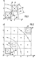
- the lines 41, 42 and the axes OX and OY define the decision zones for the states of the quarter plane shown in FIG. 1.
- the received point will move on a circle centered in 0 and passing through the particular state.
- On the circle 40 appears a position A which corresponds to the smallest distance between the circle 40 and the state (3,3).
- a detected state located at A is interpreted as being a state (3.3) whereas it is a state (3.1) or a state (1.3) with a phase difference.
- the invention defines around each state an acquisition zone 43 which does not come into contact with the circle 40 for the example chosen.
- the states selected for acquisition are states (1,1) and (3,3) because in fact the phase difference between the 4 type states ( ⁇ 1, ⁇ 1), as well as between the 4 type states ( ⁇ 3, ⁇ 3), is ⁇ / 2.
- phase error modulo ⁇ / 2
- the invention therefore selects the states which have the same symmetry as the modulation itself and defines around each state an area where the acquisition can be carried out.
- the acquisition area 43 is centered on the selected state.
- the acquisition area 44 is eccentric.
- Figure 2 shows the same type of representation for a 64 MAQ modulation.
- the acquisition problems are much more numerous due to the existence of a large number of states which can lead to a disturbance of the mechanism d 'acquisition.
- the selected states are the states (1,1), (3,3), (7,7) which have an order of symmetry identical to that of the modulation itself.
- the state (5, 5) cannot be selected because it is on the circle which passes through the states (1, 7) and (7, 1).
- an acquisition zone 43 or 44 is defined in which the acquisition must take place, this acquisition zone not coming into contact with the circles passing through the other states.
- FIG. 3 shows in B the characteristics of a phase comparator for a phase between -w / M and + ⁇ / M.
- the phase comparator delivers a voltage which is a function of the phase difference which makes it possible to control the frequency of the oscillator.
- the comparator output voltage is shown in C.
- the average value of this output voltage is zero.
- the value of the output voltage of the phase comparator is memorized using selection and acquisition means which characterize the invention.
- an acquisition circuit stores the state of the comparator output signal.
- Such a stored signal is represented in D, its average value is no longer zero. It allows the frequency correction of the oscillator to be carried out.
- the curves C and D of FIG. 3 are representative of a positive frequency deviation, that is to say a frequency of the modulated wave carrier greater than the frequency of the oscillator. For a negative frequency difference the curves C and D have an inverted shape.
- FIG. 4 represents, in the case of an MAQ 16 modulation, the state of the output signal of a phase comparator for a phase difference varying from 0 to v / 4. This domain is sufficient because the characteristic of the comparator is periodic of v / 2 and is odd.
- Such a comparator will deliver a signal which, examined over a half-period (O, w / 4), will present certain singularities depending on the state of the constellation studied.
- the half-period (0, ⁇ / 4), that is to say half of the symmetry, we note that certain states will lead to transitions by zero of the output of the comparator but for which the error of phase is not zero.
- Figure 4 shows that a state (3,1) can lead to zero transitions of the comparator output which must be eliminated to carry out the acquisition.
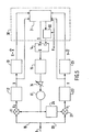
- FIG. 5 represents the block diagram of the carrier wave recovery circuit.
- the digitally modulated wave arrives at the input connection 5 and is subdivided into two channels 10 and 20 respectively in phase and in quadrature with the wave of the oscillator 17.
- the latter delivers its signal directly to the demodulator 11 of the channel in phase, and also to the demodulator 21 of the quadrature channel through the phase shifter of r / 2 24.
- the outputs of the demodulators 11 and 21 are filtered respectively in the low-pass filters 12 and 22 having the output signal respectively X and Y.
- the error signals e x and ey as well as the filtered signals X and Y enter the phase comparison device 30, which also receives the base clock H and which delivers the binary comparison signal S and the clock d 'sampling.
- These two signals enter a flip-flop 14 whose data input receives the comparison signal S and the clock input receives the sampling clock from the selection and comparison means 31 and the generation means 32 constituting the phase comparison device 30 which contains the invention.
- the output signal of the flip-flop 14 passes through a low-pass filter 15 then through an amplifier 16 to supply the control signal ⁇ ( ⁇ ) which controls the oscillator 17.
- the signals A x and Ay enter a NON-OR-exclusive gate 70 whose output enters, with the signals P x and Py, in an AND gate 71 which delivers the signal P z .
- This signal P z indicates whether the point (X, Y) received belongs or does not belong to the particular zones which it is desired to detect.
- the signal P z and the base clock H enter an AND gate 32 which delivers the sampling clock He.
- the outputs of comparators 81 and 53 enter an exclusive OR gate 85 and the outputs of comparators 83 and 63 enter an exclusive OR gate 86.
- the outputs of doors 85 and 86 enter an exclusive OR gate 87 whose output enters, with the base clock H, in an AND gate 88 which delivers a signal which serves as a clock for a flip-flop 89 whose input data come from the output of the OR-exclusive gate 85.
- This flip-flop 89 delivers an output signal S which enters the data input of the flip-flop 14 of FIG. 5, the clock of the latter being constituted by the sampling clock.
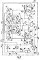
- FIG. 7 represents the logic diagram of an exemplary embodiment of the phase comparison device 30, according to the invention, in the case of zones eccentric on the diagonal states of a constellation MAQ 16.
- a first difference lies in the fact that the signals Ny, My and Qy enter a selection circuit 67 which performs the logical operation defined by:
- a second difference lies in the fact that the signals N x , M x and Q x enter a selection circuit 57 which performs the logic operation defined by:
Landscapes
- Engineering & Computer Science (AREA)
- Computer Networks & Wireless Communication (AREA)
- Signal Processing (AREA)
- Digital Transmission Methods That Use Modulated Carrier Waves (AREA)
- Communication Control (AREA)
Abstract
L'invention concerne un circuit de récupération de l'onde porteuse d'une onde modulée numériquement de symétrie 2π/M, comprenant un oscillateur commandable en tension (17) par un signal d'erreur ε(φ) afin de modifier et d'asservir la phase de l'oscillateur, l'onde modulée étant introduite sur deux voies, l'une en phase et l'autre en quadrature avec la porteuse, comprenant en série chacune : un démodulateur (11, 21), un filtre passe-bas (12, 22), des moyens de reconstruction (13, 23) d'un signal reconstruit et de détermination de l'erreur faite, la voie en quadrature comprenant en outre un déphaseur à 90° (24), les deux voies se réunissant à l'aide d'un dispositif de comparaison de phase (30) qui délivre un signal de comparaison S et une horloge d'échantillonnage He. L'invention est remarquable en ce que le dispositif de comparaison de phase comprend des moyens de sélection (31) des points reçus à l'aide de zones centrées ou excentrées sur certains états diagonaux de la constellation et des moyens de génération (32) de l'horloge He dans laquelle ont été éliminés tous les fronts actifs susceptibles de valider dans la bascule les transitions par zéro du signal de comparaison de la sortie du comparateur de phase qui ne correspondent pas à un écart de phase égale à 2kπ/M. Application : Transmission numérique, faisceaux hertziens...The invention relates to a circuit for recovering the carrier wave of a digitally modulated wave of symmetry 2π / M, comprising a voltage-controllable oscillator (17) by an error signal ε (φ) in order to modify and slave the phase of the oscillator, the modulated wave being introduced on two channels, one in phase and the other in quadrature with the carrier, each comprising in series: a demodulator (11, 21), a pass filter bottom (12, 22), means for reconstructing (13, 23) a reconstructed signal and determining the error made, the quadrature channel further comprising a 90 ° phase shifter (24), the two channels combining by means of a phase comparison device (30) which delivers a comparison signal S and a sampling clock He. The invention is remarkable in that the phase comparison device comprises means for selecting (31) the points received using zones centered or eccentric on certain diagonal states of the constellation and means for generating (32) the clock He in which all the active edges capable of validating in the flip-flop the zero transitions of the comparison signal of the output of the phase comparator which do not correspond to a phase difference equal to 2 kπ / M have been eliminated. Application: Digital transmission, radio-relay systems ...
Description
L'invention concerne un circuit de récupération de l'onde porteuse d'une onde modulée numériquement de symétrie de phase 2n/M, où M est l'ordre de la symétrie, muni de moyens d'acquisition automatiques et rapides, comprenant un oscillateur commandable en tension ayant une sortie délivrant ladite onde porteuse et une entrée de commande sur laquelle est appliqué un signal d'erreur ε(φ) afin de modifier la phase de l'oscillateur et l'asservir à celle de l'onde modulée numériquement, celle-ci étant introduite :
- . sur une première voie comprenant en série :
- - un démodulateur recevant l'onde modulée et la sortie de l'oscillateur, et délivrant un signal démodulé X1,
- - un filtre passe-bas agissant sur le signal démodulé X1 et délivrant un signal filtré X,
- - des moyens de reconstruction d'un signal X et de détermination de l'erreur ex = X-X entre les signaux X et X,
- . sur une seconde voie comprenant en série :
- - un déphaseur à 90° du signal de l'oscillateur
- - un démodulateur recevant l'onde modulée et la sortie du déphaseur et délivrant un signal démodulé Yi,
- - un filtre passe-bas agissant sur le signal démodulé Y1 et délivrant un signal filtré Y,
- - des moyens de reconstruction d'un signal Y et de détermination d'une erreur ey = Y-Y entre les signaux Y et Y, les deux voies se réunissant à l'aide d'un dispositif de comparaison de phase qui reçoit les signaux X, ex, Y, ey et une horloge de base H (horloge symbole récupérée), et qui délivre un signal de comparaison S, ainsi qu'une horloge d'échantillonnage à cadence variable qui reproduit l'horloge de base H en excluant certains fronts, le signal de comparaison entrant dans une bascule sous le contrôle de l'horloge d'échantillonnage, la sortie de la bascule étant réunie à un filtre amplificateur qui délivre le signal d'erreur ε(ø) de commande de l'oscillateur, la représentation des signaux en phase et en quadrature définissant les états d'une constellation.
- . on a first track comprising in series:
- a demodulator receiving the modulated wave and the output of the oscillator, and delivering a demodulated signal X 1 ,
- a low-pass filter acting on the demodulated signal X 1 and delivering a filtered signal X,
- means for reconstructing a signal X and for determining the error e x = XX between the signals X and X,
- . on a second channel comprising in series:
- - a 90 ° phase shifter of the oscillator signal
- a demodulator receiving the modulated wave and the output of the phase shifter and delivering a demodulated signal Y i ,
- a low-pass filter acting on the demodulated signal Y 1 and delivering a filtered signal Y,
- means for reconstructing a signal Y and for determining an error ey = YY between the signals Y and Y, the two channels coming together using a phase comparison device which receives the signals X, e x , Y, ey and a base clock H (recovered symbol clock), which delivers a comparison signal S, as well as a variable rate sampling clock which reproduces the base clock H, excluding certain edges , the comparison signal entering a flip-flop under the control of the sampling clock, the output of the flip-flop being connected to an amplifier filter which delivers the error signal ε (ø) controlling the oscillator, the representation of the signals in phase and in quadrature defining the states of a constellation.
L'invention concerne également les dispositifs où un circuit de récupération de l'onde porteuse trouve son application, tels que les dispositifs de transmission numérique, en particulier ceux pour lesquels une information, après avoir été transmise par modulation d'une onde électromagnétique est restituée par démodulation cohérente. Ces dispositifs trouvent leur application dans les modems de transmission de données, les faisceaux hertziens, les systèmes de communications spatiales ou optiques dans le cas de liaisons hétérodynes.The invention also relates to devices where a carrier wave recovery circuit finds its application, such as digital transmission devices, in particular those for which information, after having been transmitted by modulation of an electromagnetic wave is restored. by coherent demodulation. These devices find their application in data transmission modems, radio-relay systems, spatial or optical communications systems in the case of heterodyne links.
Pour effectuer la démodulation cohérente, la phase de l'onde porteuse est restituée en général à l'aide d'un oscillateur placé dans une boucle de récupération de porteuse. Cet oscillateur est commandé en tension par une version filtrée du signal de sortie d'un comparateur de phase qui détecte l'erreur de phase entre l'oscillateur et l'onde porteuse d'émission.To carry out the coherent demodulation, the phase of the carrier wave is generally restored using an oscillator placed in a carrier recovery loop. This oscillator is voltage-controlled by a filtered version of the output signal from a phase comparator which detects the phase error between the oscillator and the transmission carrier wave.
Pour des modulations numériques à grand nombre d'états, l'écart de phase entre l'oscillateur et l'onde porteuse doit être impérativement limité à des petites valeurs. La bande de bruit de la boucle de récupération est alors réduite à l'aide d'un filtrage passe-bas étroit. Cette réduction entraine un faible bruit de phase, et aussi une diminution considérable de la plage d'acquisition. Pour surmonter cet inconvénient on utilise des dispositifs d'aide à l'acquisition.For digital modulations with a large number of states, the phase difference between the oscillator and the carrier wave must be limited to small values. The noise band of the recovery loop is then reduced using narrow low-pass filtering. This reduction results in low phase noise, and also a considerable reduction in the acquisition range. To overcome this drawback, acquisition aid devices are used.
Parmi ces dispositifs on utilise couramment des discriminateurs de fréquence qui génèrent une tension qui dépend de l'écart de fréquence entre l'oscillateur et l'onde porteuse tel que celui décrit dans la demande de brevet français n° 2 552 959. Cette demande concerne un circuit de récupération de porteuse pour des modulations numériques de symétrie 2π/M dans lequel un échantillonnage à cadence variable de la sortie du comparateur de phase transforme celui-ci en discriminateur de fréquence. Cette propriété est obtenue par l'élimination des transitions par zéro de la sortie du comparateur de phase qui surviennent lorsque l'erreur de phase entre l'oscillateur et l'onde porteuse est égale à X + 2kw, M M où k et M sont des nombres entiers.Among these devices, frequency discriminators are commonly used which generate a voltage which depends on the frequency difference between the oscillator and the carrier wave such as that described in the French patent application. çais n ° 2 552 959. This request relates to a carrier recovery circuit for digital modulations of 2π / M symmetry in which a variable rate sampling of the output of the phase comparator transforms it into frequency discriminator. This property is obtained by eliminating the zero transitions of the phase comparator output which occur when the phase error between the oscillator and the carrier wave is equal to X + 2k w , MM where k and M are whole numbers.
Or en présence de modulations numériques d'amplitude de deux porteuses en quadrature à multi-états, le discriminateur de fréquence, décrit dans cette demande, présente des inconvénients, son gain se trouvant dégradé, car il subsiste sur la sortie échantillonnée du comparateur de phase des transitions par zéro qui sont prises en compte, et qui ne correspondent pas à une erreur de phase nulle. En effet, ce discri- minateur de fréquence génère une horloge d'échantillonnage, à partir d'une horloge de base H, dans laquelle certains fronts actifs de cette dernière sont éliminés. Cette élimination survient lorsque l'on détecte des transitions par zéro pour lesquelles l'écart de phase entre l'oscillateur et l'onde porteuse est égal à Ξ + 2kπ.However in the presence of digital amplitude modulations of two carriers in quadrature with multi-states, the frequency discriminator, described in this request, has drawbacks, its gain being degraded, because it remains on the sampled output of the phase comparator transitions by zero which are taken into account, and which do not correspond to a zero phase error. Indeed, it discrimi - Frequency denominator generates a sampling clock from a basic clock H, wherein some active edges of the latter are eliminated. This elimination occurs when zero transitions are detected for which the phase difference between the oscillator and the carrier wave is equal to Ξ + 2kπ.
M M Mais il apparaît à l'expérience, dans des modulations de phase et d'amplitude, qu'il existe d'autres transitions par zéro à la sortie du comparateur de phase qui mettent en défaut une acquisition correcte de l'onde porteuse. Par exemple dans le cas d'une modulation MAQ 16, la sortie des comparateurs de phase couramment utilisés présentent des transitions par zéro alors que l'écart de phase est égal à 8 = Arc tg 1/3 pour les états (3,1), (-1,3), (-3,-1), (1,-3). D'autres états présentent un comportement analogue. De plus, avec un nombre d'états de modulation plus important, le nombre de ces transitions par zéro indésirables va croître, et ceci entraîne une détérioration des performances du discriminateur.M M But it appears from experience, in phase and amplitude modulations, that there are other zero transitions at the output of the phase comparator which put in error a correct acquisition of the carrier wave. For example in the case of an MAQ 16 modulation, the output of the phase comparators commonly used have zero transitions while the phase difference is equal to 8 =
Le but de l'invention est donc d'éviter cette dégradation en supprimant la prise en compte de toutes les transitions par zéro indésirables.The object of the invention is therefore to avoid this dice gradation by removing the taking into account of all the undesirable zero transitions.
Pour cela l'invention telle que définie dans le préambule est remarquable en ce que le circuit de récupération de l'onde porteuse possède un dispositif de comparaison de phase qui comprend des moyens de sélection des points reçus à l'aide de zones de sélection situées autour de certains états diagonaux de la constellation de sorte que les cercles passant par les états non-diagonaux ne coupent pas lesdites zones de sélection, et que les zones tracées autour des points de type (i1, ±1) ne viennent pas en contact avec les axes OX, OY de la constellation, et des moyens de génération de l'horloge d'échantillonnage dans laquelle ont été éliminés tous les fronts actifs susceptibles de valider dans la bascule les transitions par zéro du signal de comparaison de la sortie du comparateur de phase qui ne correspondent pas à un écart de phase égal à 2kπ/M, où k et M sont des nombres entiers.For this, the invention as defined in the preamble is remarkable in that the carrier wave recovery circuit has a phase comparison device which includes means for selecting the points received using selection zones located around certain diagonal states of the constellation so that the circles passing through the non-diagonal states do not intersect said selection areas, and that the areas drawn around the points of type (i1, ± 1) do not come into contact with the axes OX, OY of the constellation, and means for generating the sampling clock in which all the active edges capable of validating in the flip-flop the zero transitions of the comparison signal of the comparator output are eliminated. phase which do not correspond to a phase difference equal to 2kπ / M, where k and M are whole numbers.
Ce dispositif est basé sur la mémorisation du signe de la sortie du comparateur de phase lorsque la valeur absolue de l'écart de phase dépasse une certaine valeur. Cette mémorisation s'effectue dans une bascule dont la sortie présente une tension qui reste constante entre deux transitions par zéro reconnues valables. Cette tension constante est de même signe que l'écart de fréquence entre l'oscillateur et l'onde porteuse.This device is based on the memorization of the sign of the output of the phase comparator when the absolute value of the phase difference exceeds a certain value. This storage takes place in a flip-flop whose output has a voltage which remains constant between two zero transitions recognized as valid. This constant voltage is the same sign as the frequency difference between the oscillator and the carrier wave.
Pour effectuer la mémorisation, on définit des zones pour lesquelles l'erreur de phase à la sortie du comparateur s'annule une seule fois, le signe de la sortie du comparateur de phase restant identique au signe de l'erreur de phase.To carry out the storage, zones are defined for which the phase error at the output of the comparator is canceled out only once, the sign of the output of the phase comparator remaining identical to the sign of the phase error.
Ce circuit de récupération de l'onde porteuse fait appel à un comparateur de phase qui possède les propriétés suivantes :
- - sa caractéristique s'annule pour une erreur de phase nulle ;
- - sa caractéristique est périodique de période 2π/M où M est l'ordre de symétrie de la modulation.
- - its characteristic is canceled for a zero phase error;
- - its characteristic is periodic of period 2π / M where M is the order of symmetry of the modulation.
L'invention trouve son application pour des modulations numériques de symétrie de phase 2n/M où M est l'ordre de symétrie de la constellation. Ainsi, une modulation de phase à 4 états présente une symétrie d'ordre 4, pour une modulation de phase à 8 états la symétrie est d'ordre 8, pour une modulation de phase et d'amplitude de deux porteuses en quadrature MAQ 16, la symétrie est d'ordre 4.The invention finds its application for digital modulations of phase symmetry 2n / M where M is the order of symmetry of the constellation. Thus, a 4-state phase modulation has a 4-order symmetry, for an 8-state phase modulation the symmetry is of an 8 order, for a phase and amplitude modulation of two carriers in quadrature MAQ 16, symmetry is of order 4.
Mais l'invention présente ses avantages déterminants dans le cas des modulations d'amplitude et de phase pour lesquelles les écarts de phase entre certains points de la constellation sont inférieurs à la symétrie 2r/M. Ainsi en modulation MAQ 16 la symétrie est de π/2, mais l'écart de phase entre les états (1,1) et (1,3) est de π/4 - arc (tg.1/3) donc inférieur à w/2.However, the invention has its decisive advantages in the case of amplitude and phase modulations for which the phase differences between certain points of the constellation are less than the 2r / M symmetry. Thus in MAQ 16 modulation the symmetry is π / 2, but the phase difference between the states (1,1) and (1,3) is π / 4 - arc (tg. 1/3) therefore less than w / 2.
Au cours de la période d'acquisition de la porteuse, l'onde modulée numériquement va pouvoir présenter tous les points de la constellation. L'invention élimine donc tous les points reçus qui sont susceptibles de provoquer une acquisition erronée.During the carrier acquisition period, the digitally modulated wave will be able to present all the points of the constellation. The invention therefore eliminates all the points received which are liable to cause an erroneous acquisition.
Ainsi, le circuit de récupération de l'onde porteuse, selon l'invention, possède des moyens de sélection des points reçus à l'aide de zones situées autour de certains états de la constellation.Thus, the carrier wave recovery circuit, according to the invention, has means for selecting the points received using zones located around certain states of the constellation.
Cette sélection s'effectue en déterminant l'appartenance ou la non-appartenance des points reçus à des zones possédant les propriétés suivantes :
- - tout point reçu dans ces zones présente un écart de phase avec le point émis, tel que la valeur absolue de cet écart de phase reste inférieure, à 2ku/M près, à une valeur choisie, ce qui permet d'éliminer les transitions par zéro à ku/M ;
- - tout signal reconstruit à partir d'un point reçu dans ces zones est identique à 2kπ/M près, au signal émis correspondant.
- - any point received in these zones has a phase difference with the transmitted point, such that the absolute value of this phase difference remains less, to within 2ku / M, than a chosen value, which makes it possible to eliminate the transitions by zero to ku / M;
- - any signal reconstructed from a point received in these areas is identical to within 2kπ / M, with the corresponding transmitted signal.
Ainsi l'information prise en compte est seulement celle fournie par les points reçus dans ces zones. En modulation MAQ ces zones peuvent être formées de carrés centrés sur des états diagonaux de la modulation. D'une manière plus générale, les zones peuvent être constituées d'un contour fermé, borné en X et Y, entourant ces états diagonaux.Thus the information taken into account is only that provided by the points received in these areas. In MAQ modulation, these zones can be formed by squares centered on diagonal states of the modulation. More generally, the zones can consist of a closed contour, bounded in X and Y, surrounding these diagonal states.
Pour déterminer l'appartenance à ces zones, puis la prise en compte de l'information y afférente, l'invention construit un dispositif de comparaison de phase qui s'insère dans un circuit de récupération d'une onde porteuse. Pour cela l'onde modulée numériquement est introduite simultanément sur deux démodulateurs, recevant également l'un la sortie de l'oscillateur et l'autre cette même sortie mais après avoir traversé un déphaseur de t/2 et délivrant respectivement les signaux démodulés X, et Y1. Ceux-ci sont filtrés et fournissent respectivement les signaux X (en phase) et Y (en quadrature) à partir desquels des signaux reconstruits X et Y sont obtenus. Les erreurs ex et ey entre les signaux filtrés et reconstruits, ainsi que les signaux X et Y, sont introduits dans le dispositif de comparaison de phase qui délivre un signal binaire indiquant le signe de la caractéristique du comparateur de phase pour I'angle φ apparaissant entre l'onde modulée reçue et l'onde de l'oscillateur. Ce signal binaire est introduit dans une bascule sous le contrôle de l'horloge d'échantillonnage qui ne comprend que les fronts actifs souhaités. La sortie de la bascule est filtrée puis amplifiée pour délivrer le signal de commande ε(φ) pour l'oscillateur. Le dispositif de comparaison génère un signal Pz caractérisant la sélection des zones qui sert à construire l'horloge d'échantillonnage.To determine membership in these zones, then taking into account the information relating thereto, the invention constructs a phase comparison device which is inserted into a circuit for recovering a carrier wave. For this, the digitally modulated wave is introduced simultaneously on two demodulators, one also receiving the output of the oscillator and the other this same output but after having passed through a phase shifter of t / 2 and respectively delivering the demodulated signals X, and Y 1 . These are filtered and respectively provide the signals X (in phase) and Y (in quadrature) from which reconstructed signals X and Y are obtained. The errors e x and ey between the filtered and reconstructed signals, as well as the signals X and Y, are introduced into the phase comparison device which delivers a binary signal indicating the sign of the characteristic of the phase comparator for the angle φ appearing between the received modulated wave and the oscillator wave. This binary signal is introduced into a flip-flop under the control of the sampling clock which only includes the desired active edges. The output of the rocker is filtered then amplified to deliver the control signal ε (φ) for the oscillator. The comparison device generates a signal P z characterizing the selection of the zones which is used to construct the sampling clock.
L'invention sera mieux comprise à l'aide des dessins annexés, donnés à titre d'exemples non limitatifs, et qui représentent :
- Figure 1 : la représentation, dans un quart de plan, de la constellation d'une onde MAQ 16.
- Figure 2 : la représentation, dans un quart de plan, de la constellation d'une onde MAQ 64.
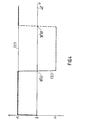
- Figure 3 : une représentation de la caractéristique du comparateur de phase et des variations, avec la phase, du signal de sortie du comparateur de phase avant et après mémorisation dans une bascule.
- Figure 4 : une représentation des variations, avec la phase, du signal de sortie du comparateur de phase, pour certains états de la constellation en MAQ 16.
- Figure 5 : un schéma-bloc du circuit de récupération de l'onde porteuse selon l'invention.
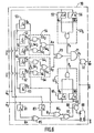
- Figure 6 : un schéma logique du dispositif de comparaison de phase selon l'invention dans le cas de zones carrées centrées sur les états de la constellation.
- Figure 7 : un schéma logique du dispositif de comparaison de phase selon l'invention dans le cas de zones carrées excentrées sur les états de la constellation.
- Figure 1: the representation, in a quarter of a plane, of the constellation of an MAQ wave 16.
- Figure 2: the representation, in a quarter of a plane, of the constellation of an MAQ 64 wave.
- FIG. 3: a representation of the characteristic of the phase comparator and of the variations, with the phase, of the output signal of the phase comparator before and after storage in a flip-flop.
- Figure 4: a representation of the variations, with the phase, of the output signal of the phase comparator, for certain states of the constellation in MAQ 16.
- Figure 5: a block diagram of the carrier wave recovery circuit according to the invention.
- Figure 6: a logic diagram of the phase comparison device according to the invention in the case of square areas centered on the states of the constellation.
- Figure 7: a logic diagram of the phase comparison device according to the invention in the case of eccentric square zones on the states of the constellation.
La figure 1 représente dans un quart de plan XOY la partie de constellation MAQ 16. Elle présente quatre états (1,1), (3,1), (1,3), (3,3) dans ce quart de plan. Pour le plan total cette constellation a une symétrie 2π = π. Elle pré-M 2 sente un écart de phase minimal tel que
Les droites 41, 42 et les axes OX et OY définissent les zones de décision pour les états du quart de plan représentés sur la figure 1.The
Selon la variation de phase de l'onde modulée incidente par rapport à l'oscillateur, pour un état particulier de la constellation, le point reçu va se déplacer sur un cercle centré en 0 et passant par l'état particulier. Sur le cercle 40 apparaît une position A qui correspond à la distance la plus faible entre le cercle 40 et l'état (3,3). Un état détecté se situant en A est interprété comme étant un état (3,3) alors qu'il s'agit d'un état (3,1) ou d'un état (1,3) avec un écart de phase. Pour cela l'invention définit autour de chaque état une zone d'acquisition 43 qui n'entre pas en contact avec le cercle 40 pour l'exemple choisi. Dans le cas de la modulation MAQ 16, les états sélectionnés en vue de l'acquisition sont les états (1,1) et (3,3) car en effet l'écart de phase entre les 4 états de type (±1, ±1), ainsi qu'entre les 4 états de type (±3, ±3), est de π/2. Par contre, entre les 8 états de type (±1, ±3) et (±3, ±1) l'écart de phase minimal est de 2.Arc tg(1/3)=36°87. Une erreur de phase β, entre l'émission et la réception, supérieure à environ 19° par exemple, ramène un point (+1, +3) dans la zone de décision du point (-1, +3). Par conséquent avec les points (i1, ±3) et (±3, ±1) une erreur de phase de β ne peut être distinguée d'une erreur 2.(Arc tg1/3)-β ou d'une erreur de phase 2α-β (pour a, voir figure 1). Lors de l'émission d'un état (+3, +1) et pour une erreur de phase de +48° par exemple, le point peut être détecté comme un état (+1, +3) avec une erreur de phase estimée à -5°. De même pour un état (3, -1), avec une erreur de phase de + 48° par exemple, le point peut être détecté comme un état (+3, +1) avec un erreur de phase estimée à +11°. Ainsi, si on se fixe de prendre en compte l'erreur de phase, modulo π/2, seulement lorsqu'elle est inférieure à 15° par exemple, il est clair que l'on ne peut pas prendre en compte les états non-diagonaux, car il serait impossible de déterminer si l'erreur de phase détectée est à l'intérieur de l'intervalle prédéterminé.According to the phase variation of the incident modulated wave with respect to the oscillator, for a particular state of the constellation, the received point will move on a circle centered in 0 and passing through the particular state. On the
L'invention sélectionne donc les états qui présentent la même symétrie que la modulation elle-même et définit autour de chaque état une zone où l'acquisition peut être effectuée. La zone d'acquisition 43 est centrée sur l'état sélectionné. Par contre, la zone d'acquisition 44 est excentrée.The invention therefore selects the states which have the same symmetry as the modulation itself and defines around each state an area where the acquisition can be carried out. The
La figure 2 indique le même type de représentation pour une modulation MAQ 64. Dans ce cas les problèmes d'acquisition sont beaucoup plus nombreux du fait de l'existence d'un grand nombre d'états qui peuvent conduire à une perturbation du mécanisme d'acquisition. Dans ce cas, les états sélectionnés sont les états (1,1),(3,3),(7,7) qui possèdent un ordre de symétrie identique à celui de la modulation elle-même. L'état (5, 5) ne peut pas être sélectionné car il se trouve sur le cercle qui passe par les états (1, 7) et (7, 1). Autour de chacun des états sélectionnés on définit une zone d'acquisition 43 ou 44 dans laquelle l'acquisition doit s'effectuer, cette zone d'acquisition n'entrant pas en contact avec les cercles passant par les autres états.Figure 2 shows the same type of representation for a 64 MAQ modulation. In this case, the acquisition problems are much more numerous due to the existence of a large number of states which can lead to a disturbance of the mechanism d 'acquisition. In this case, the selected states are the states (1,1), (3,3), (7,7) which have an order of symmetry identical to that of the modulation itself. The state (5, 5) cannot be selected because it is on the circle which passes through the states (1, 7) and (7, 1). Around each of the selected states, an
La figure 3 représente en B les caractéristiques d'un comparateur de phase pour une phase comprise entre -w/M et +π/M. De part et d'autre du point o (écart de phase nul), le comparateur de phase délivre une tension fonction de l'écart de phase qui permet d'asservir la fréquence de l'oscillateur. La tension de sortie du comparateur est représentée en C. La valeur moyenne de cette tension de sortie est nulle. Pour effectuer la correction de fréquence de l'oscillateur, on mémorise la valeur de la tension de sortie du comparateur de phase à l'aide de moyens de sélection et d'acquisition qui caractérisent l'invention. Lorsque la valeur absolue de l'écart de phase dépasse une valeur 80, ce qui correspond au franchissement de la zone d'acquisition choisie, un circuit d'acquisition mémorise l'état du signal de sortie du comparateur. Un tel signal mémorisé est représenté en D, sa valeur moyenne n'est plus nulle. Elle permet d'effectuer la correction de fréquence de l'oscillateur. Les courbes C et D de la figure 3 sont représentatives d'un écart de fréquence positif c'est-à-dire une fréquence de porteuse d'onde modulée plus grande que la fréquence de l'oscillateur. Pour un écart de fréquence négatif les courbes C et D présentent une allure inversée.FIG. 3 shows in B the characteristics of a phase comparator for a phase between -w / M and + π / M. On either side of point o (zero phase difference), the phase comparator delivers a voltage which is a function of the phase difference which makes it possible to control the frequency of the oscillator. The comparator output voltage is shown in C. The average value of this output voltage is zero. To effect the frequency correction of the oscillator, the value of the output voltage of the phase comparator is memorized using selection and acquisition means which characterize the invention. When the absolute value of the phase difference exceeds a value 8 0 , which corresponds to the crossing of the chosen acquisition area, an acquisition circuit stores the state of the comparator output signal. Such a stored signal is represented in D, its average value is no longer zero. It allows the frequency correction of the oscillator to be carried out. The curves C and D of FIG. 3 are representative of a positive frequency deviation, that is to say a frequency of the modulated wave carrier greater than the frequency of the oscillator. For a negative frequency difference the curves C and D have an inverted shape.
La figure 4 représente, dans le cas d'une modulation MAQ 16, l'état du signal de sortie d'un comparateur de phase pour un écart de phase variant de 0 à v/4. Ce domaine est suffisant car la caractéristique du comparateur est périodique de v/2 et est impaire. Le comparateur considéré est un comparateur d'un type classique qui délivre un signal de sortie S tel que S = -sgn(ey).sgn(X) si sgn(ey).sgn(X) est de signe opposé à sgn(ex).sgn(Y), et tel que S garde la valeur présente à l'instant précédent dans le cas contraire. Un tel comparateur va délivrer un signal qui, examiné sur une demi-période (O,w/4), va présenter certaines singularités selon l'état de la constellation étudié. Ainsi en limitant l'analyse à la demi-période (0,π/4), soit la moitié de la symétrie, on constate que certains états vont conduire à des transitions par zéro de la sortie du comparateur mais pour lesquelles l'erreur de phase n'est pas nulle. Ainsi la figure 4 montre qu'un état (3,1) peut conduire à des transitions par zéro de la sortie du comparateur qui doivent être éliminées pour effectuer l'acquisition.FIG. 4 represents, in the case of an MAQ 16 modulation, the state of the output signal of a phase comparator for a phase difference varying from 0 to v / 4. This domain is sufficient because the characteristic of the comparator is periodic of v / 2 and is odd. The comparator considered is a comparator of a conventional type which delivers an output signal S such that S = -sgn (ey) .sgn (X) if sgn (ey) .sgn (X) is of opposite sign to sgn (e x ) .sgn ( Y), and such that S keeps the value present at the previous instant in the opposite case. Such a comparator will deliver a signal which, examined over a half-period (O, w / 4), will present certain singularities depending on the state of the constellation studied. Thus by limiting the analysis to the half-period (0, π / 4), that is to say half of the symmetry, we note that certain states will lead to transitions by zero of the output of the comparator but for which the error of phase is not zero. Thus Figure 4 shows that a state (3,1) can lead to zero transitions of the comparator output which must be eliminated to carry out the acquisition.
La figure 5 représente le schéma-bloc du circuit de récupération de l'onde porteuse. L'onde modulée numériquement arrive sur la connexion d'entrée 5 et se subdivise en deux voies 10 et 20 respectivement en phase et en quadrature avec l'onde de l'oscillateur 17. Celui-ci délivre son signal directement au démodulateur 11 de la voie en phase, et également au démodulateur 21 de la voie en quadrature à travers le déphaseur de r/2 24. Les sorties des démodulateurs 11 et 21 sont filtrées respectivement dans les filtres passe-bas 12 et 22 ayant pour signal de sortie respectivement X et Y. Ces signaux pénètrent dans des circuits de reconstruction, respectivement 13 et 23, qui délivrent respectivement les erreurs ex = X-X et ey = Y-Y entre les signaux filtrés X et Y et les signaux reconstruits X et Y.FIG. 5 represents the block diagram of the carrier wave recovery circuit. The digitally modulated wave arrives at the
Les signaux d'erreur ex et ey ainsi que les signaux filtrés X et Y pénètrent dans le dispositif de comparaison de phase 30, qui reçoit également l'horloge de base H et qui délivre le signal binaire de comparaison S et l'horloge d'échantillonnage. Ces deux signaux entrent dans une bascule 14 dont l'entrée des données reçoit le signal de comparaison S et l'entrée d'horloge reçoit l'horloge d'échantillonnage issue des moyens de sélection et de comparaison 31 et des moyens de génération 32 constituant le dispositif de comparaison de phase 30 qui contient l'invention. Le signal de sortie de la bascule 14 passe dans un filtre passe-bas 15 puis dans un amplificateur 16 pour fournir le signal de commande ε(φ) qui contrôle l'oscillateur 17.The error signals e x and ey as well as the filtered signals X and Y enter the
La figure 6 représente le schéma logique d'un exemple de réalisation du dispositif de comparaison de phase 30 selon l'invention dans le cas de zones carrées centrées sur les états diagonaux d'une constellation MAQ 16. Il reçoit en entrée les signaux X, Y, ex = X-X, ey = Y-Y et l'horloge de base H. Il délivre le signal S et l'horloge d'échantillonnage He. Le signal Y entre dans :
- - un comparateur 61 à seuil -2 qui délivre le signal Ty
- -
un comparateur 62 à seuil 2 qui délivre le signal Ry - -
un comparateur 63 à seuil 0 qui délivre le signal Qy.
- - a comparator 61 at threshold -2 which delivers the signal Ty
- - a
comparator 62 at threshold 2 which delivers the signal Ry - - a
comparator 63 atthreshold 0 which delivers the signal Qy.
Les signaux Ty, Ry, Qy entrent dans un circuit de sélection 64 qui effectue l'opération logique définie par Ay = Ry.Qy + Ty.Qy, où le symbole (.) représente la fonction logique ET et le symbole (+) représente la fonction logique OU. Ceci est effectué à l'aide d'une porte ET 642 qui reçoit Ry et Qy, d'un inverseur 643 qui délivre Qy, signal inverse du signal d'entrée Qy, une porte ET 641 qui reçoit les signaux Ty et Qy, les sorties des portes ET 641 et ET 642 entrant dans une porte OU 644 qui délivre le signal Ay.The signals Ty, Ry, Qy enter a selection circuit 64 which performs the logic operation defined by Ay = Ry.Qy + Ty.Qy, where the symbol (.) Represents the logic function AND and the symbol (+) represents the OR logic function. This is done using an AND gate 64 2 which receives Ry and Qy, an inverter 64 3 which delivers Qy, reverse signal of the input signal Qy, an AND gate 64 1 which receives the signals Ty and Qy, the outputs of AND gates 64 1 and AND 64 2 entering an OR gate 64 4 which delivers the signal Ay.
Le signal X est traité de la même façon que le signal Y. Il entre dans :
- -
un comparateur 51 à seuil -2 qui délivre le signal Tx - -
un comparateur 52 à seuil 2 qui délivre le signal Rx - -
un comparateur 53 à seuil 0 qui délivre le signal Qx.
- - a
comparator 51 at threshold -2 which delivers the signal T x - - a
comparator 52 at threshold 2 which delivers the signal R x - - a
comparator 53 atthreshold 0 which delivers the signal Q x .
Les signaux Tx, Rx et Qx entrent dans un circuit de sélection 54 qui effectue l'opération logique définie par Ax = Rx.Qx + Tx.Qx.The signals T x , R x and Q x enter a
Ceci est effectué à l'aide d'une porte ET 542 qui reçoit Rx et Qx, d'un inverseur 543 qui délivre Qx, signal inverse du signal d'entrée Qx, une porte ET 541 qui reçoit les signaux
D'autre part le signal ey entre dans :
- -
un comparateur 65 à seuil -a qui délivre le signal Ny - - un comparateur 66 à seuil a qui délivre le signal My Les signaux Ny et My entrent dans une
porte ET 675 qui effectue l'opération logique définie par Py = Ny.M y.
- - a
comparator 65 at threshold -a which delivers the signal Ny - a comparator 66 with threshold a which delivers the signal My The signals Ny and My enter an AND
gate 67 5 which performs the logic operation defined by P y = N y .M y .
De la même façon le signal ex entre dans :
- -
un comparateur 55 à seuil -a qui délivre le signal Nx - -
un comparateur 56 à seuil a qui délivre le signal Mx. Les signaux Nx et Mx entrent dans uneporte ET 575 qui effectue l'opération logique définie par Px = Nx.Mx.
- - a
comparator 55 at threshold -a which delivers the signal N x - - A
comparator 56 with threshold a which delivers the signal M x . The signals N x and M x enter an ANDgate 57 5 which performs the logic operation defined by P x = N x . M x.
Les signaux Ax et Ay entrent dans une porte NON-OU-exclusif 70 dont la sortie entre, avec les signaux Px et Py, dans une porte ET 71 qui délivre le signal Pz. Ce signal Pz indique si le point (X, Y) reçu appartient ou n'appartient pas aux zones particulières que l'on désire détecter.The signals A x and Ay enter a NON-OR-
Le signal Pz et l'horloge de base H entrent dans une porte ET 32 qui délivre l'horloge d'échantillonnage He.The signal P z and the base clock H enter an AND
D'autre part on détermine le signe des signaux exi ey, X, Y afin de déterminer, à un instant donné, le signal de sortie S tel que :
- - le signal ey dans
un comparateur 81 - - le signal ex dans
un comparateur 83.
- - the ey signal in a
comparator 81 - - the signal e x in a
comparator 83.
Les sorties des comparateurs 81 et 53 entrent dans une porte OU-exclusif 85 et les sorties des comparateurs 83 et 63 entrent dans une porte OU-exclusif 86. Les sorties des portes 85 et 86 entrent dans une porte OU-exclusif 87 dont la sortie entre, avec l'horloge de base H, dans une porte ET 88 qui délivre un signal qui sert d'horloge à une bascule 89 dont les données d'entrée sont issues de la sortie de la porte OU-exclusif 85. Cette bascule 89 délivre un signal de sortie S qui entre sur l'entrée des données de la bascule 14 de la figure 5, l'horloge de cette dernière étant constituée par l'horloge d'échantillonnage.The outputs of
La figure 7 représente le schéma logique d'un exemple de réalisation du dispositif de comparaison de phase 30, selon l'invention, dans le cas de zones excentrées sur les états diagonaux d'une constellation MAQ 16.FIG. 7 represents the logic diagram of an exemplary embodiment of the
Une première différence se situe dans le fait que les signaux Ny, My et Qy entrent dans un circuit de sélection 67 qui effectue l'opération logique définie par :
Ceci est effectué à l'aide d'une porte ET 672 qui reçoit Ny et Qy, d'un inverseur 673 qui délivre Qy, signal inverse du signal d'entrée Qy, une porte ET 671 qui reçoit les signaux My et Qy, les sorties des portes ET 671 et 672 entrant dans une porte OU 674 qui délivre le signal Py.This is done using an AND
Une seconde différence se situe dans le fait que les signaux Nx, Mx et Qx entrent dans un circuit de sélection 57 qui effectue l'opération logique définie par :
Ceci est effectué à l'aide d'une porte ET 572 qui reçoit Nx et Qx, d'un inverseur 573 qui délivre Qx, signal inverse du signal d'entrée Qx, une porte ET 571 qui reçoit les signaux
Tous les signaux sont ensuite traités de manière analogue à celle utilisée pour la figure 6.All the signals are then processed in a similar manner to that used for FIG. 6.
Bien évidemment les schémas logiques donnés sur les figures 6 et 7 sont des exemples non limitatifs et tout autre schéma logique correspondant à l'objet de l'invention en fait également partie.Obviously the logic diagrams given in FIGS. 6 and 7 are nonlimiting examples and any other logic diagram corresponding to the object of the invention also forms part of it.
Claims (5)
et sur la voie en quadrature,
et un circuit ET recevant la sortie du circuit NON-OU-exclusif et les signaux Px et Py, et délivrant le signal Pz qui entre dans un circuit ET ainsi que l'horloge de base H pour délivrer l'horloge d'échantillonnage.4. Circuit for recovering the carrier wave of a digitally modulated wave of phase symmetry 2π / M according to one of claims 1 to 3, characterized in that the means for selecting the received points and the means for generating the sampling clock include: on the phasing channel,
and on the quadrature track,
and an AND circuit receiving the output of the NOT-OR-exclusive circuit and the signals P x and Py, and delivering the signal P z which enters an AND circuit as well as the base clock H for issue the sampling clock.
et un circuit ET recevant la sortie du circuit NON-OU-exclusif et les signaux Px et Py, et délivrant le signal Pz qui entre dans un circuit ET ainsi que l'horloge de base H pour délivrer l'horloge d'échantillonnage.
and an AND circuit receiving the output of the NOT-OR-exclusive circuit and the signals P x and Py, and delivering the signal P z which enters an AND circuit as well as the base clock H to deliver the sampling clock .
Applications Claiming Priority (2)
| Application Number | Priority Date | Filing Date | Title |
|---|---|---|---|
| FR8506561 | 1985-04-30 | ||
| FR8506561A FR2581277A1 (en) | 1985-04-30 | 1985-04-30 | VEHICLE WAVE RECOVERY CIRCUIT FOR DIGITAL TRANSMISSION SYSTEMS |
Publications (2)
| Publication Number | Publication Date |
|---|---|
| EP0200271A1 true EP0200271A1 (en) | 1986-11-05 |
| EP0200271B1 EP0200271B1 (en) | 1990-01-31 |
Family
ID=9318824
Family Applications (1)
| Application Number | Title | Priority Date | Filing Date |
|---|---|---|---|
| EP86200712A Expired - Lifetime EP0200271B1 (en) | 1985-04-30 | 1986-04-25 | Carrier recovery circuit for digital transmission systems |
Country Status (9)
| Country | Link |
|---|---|
| US (1) | US4687999A (en) |
| EP (1) | EP0200271B1 (en) |
| JP (1) | JPH0793644B2 (en) |
| AU (1) | AU5676986A (en) |
| CA (1) | CA1256953A (en) |
| DE (1) | DE3668741D1 (en) |
| FI (1) | FI86126C (en) |
| FR (1) | FR2581277A1 (en) |
| NO (1) | NO172670C (en) |
Cited By (5)
| Publication number | Priority date | Publication date | Assignee | Title |
|---|---|---|---|---|
| FR2620885A1 (en) * | 1987-09-18 | 1989-03-24 | Alcatel Thomson Faisceaux | METHOD FOR DETECTING FALSE ATTACHMENTS OF THE SIGNAL REFERENCE ON THE SIGNAL TO BE DEMODULATED IN COHERENT DIGITAL DEMODULATION AND DEVICE IMPLEMENTING SAID METHOD |
| GB2282030A (en) * | 1993-09-14 | 1995-03-22 | Plessey Semiconductors Ltd | Direct conversion receivers |
| EP0703687A1 (en) * | 1994-09-23 | 1996-03-27 | France Telecom | Carrier recovery for PSK signals |
| EP0719002A1 (en) * | 1994-12-22 | 1996-06-26 | ALCATEL BELL Naamloze Vennootschap | Carrier recovery processor |
| EP1940104A3 (en) * | 2006-12-29 | 2012-07-25 | Trident Microsystems (Far East) Ltd. | Method and device for determining a symbol when receiving a signal coupled with a quadrature signal pair for QAM frequency control and/or rotation control |
Families Citing this family (36)
| Publication number | Priority date | Publication date | Assignee | Title |
|---|---|---|---|---|
| DE3619744A1 (en) * | 1986-06-12 | 1987-12-17 | Ant Nachrichtentech | METHOD FOR OBTAINING A PHASE DIFFERENTIAL SIGNAL |
| US4860320A (en) * | 1986-06-12 | 1989-08-22 | Ant Nachrichtentechnik Gmbh | Method for recovering a control signal for controlling the phase of a local carrier signal |
| EP0281652B1 (en) * | 1987-03-10 | 1990-12-05 | ANT Nachrichtentechnik GmbH | Method for obtaining a phase difference signal |
| US4736386A (en) * | 1987-04-06 | 1988-04-05 | Rockwell International Corporation | Carrier out-of-lock detector apparatus |
| US4771438A (en) * | 1987-08-04 | 1988-09-13 | Hayes Microcomputer Products, Inc. | Method and apparatus for phase reference recovery in high speed fast turnaround modem |
| FR2621188B1 (en) * | 1987-09-25 | 1989-12-29 | Labo Electronique Physique | CIRCUIT FOR RECOVERING THE CARRIER WAVE OF DIGITAL TRANSMISSION SYSTEMS |
| FR2627653B1 (en) * | 1988-02-18 | 1994-04-08 | Alcatel Thomson Faisceaux Hertzi | PROCESS OF SERVOTING THE REGENERATION MOMENT IN A DIGITAL TRANSMISSION USING A CARRIER MODULATION ACCORDING TO TWO QUADRATURE AXES AND DEVICE FOR CARRYING OUT SAID METHOD |
| JPH02217045A (en) * | 1989-02-17 | 1990-08-29 | Fujitsu Ltd | Signal point arranging system |
| US4959844A (en) * | 1989-10-24 | 1990-09-25 | Amp Incorporated | Clock recovery circuit for digital demodulator |
| US5287351A (en) * | 1990-11-27 | 1994-02-15 | Scientific-Atlanta, Inc. | Method and apparatus for minimizing error propagation in correlative digital and communication system |
| AU1918892A (en) * | 1991-05-10 | 1992-12-30 | Echelon Corporation | Power line communication while avoiding determinable interference harmonics |
| US5271041A (en) * | 1992-03-16 | 1993-12-14 | Scientific-Atlanta, Inc. | Method and apparatus for QPR carrier recovery |
| US5528632A (en) * | 1994-07-28 | 1996-06-18 | Motorola, Inc. | Non-complex dual-correlation phase reversal detector and method |
| JP3540393B2 (en) * | 1994-10-31 | 2004-07-07 | 三洋電機株式会社 | Costas Loop |
| AUPN455695A0 (en) * | 1995-08-01 | 1995-08-24 | Canon Kabushiki Kaisha | Qam spread spectrum demodulation system |
| US5640425A (en) * | 1995-12-26 | 1997-06-17 | Golden Bridge Technology, Inc. | Fast-acting costas loop |
| DE59709234D1 (en) * | 1997-07-31 | 2003-03-06 | Micronas Semiconductor Holding | Carrier control loop for a receiver of digitally transmitted signals |
| DE19733732C2 (en) * | 1997-08-04 | 1999-05-12 | Siemens Ag | Method to support simple synchronization to the carrier of an energy-blown QPSK signal |
| US6738429B1 (en) * | 1999-06-01 | 2004-05-18 | Harris Corporation | Decision-directed carrier frequency detector and method for QAM |
| EP1503500B1 (en) * | 2003-07-28 | 2006-06-28 | Frank Dr.-Ir. Op 't Eynde | A phase-locked loop |
| US7355470B2 (en) | 2006-04-24 | 2008-04-08 | Parkervision, Inc. | Systems and methods of RF power transmission, modulation, and amplification, including embodiments for amplifier class transitioning |
| US7327803B2 (en) | 2004-10-22 | 2008-02-05 | Parkervision, Inc. | Systems and methods for vector power amplification |
| US8041538B2 (en) * | 2005-07-05 | 2011-10-18 | Stmicroelectronics S.A. | Estimating of the amplitude of a noisy binary signal |
| RU2296432C1 (en) * | 2005-10-07 | 2007-03-27 | Военно-космическая академия имени А.Ф. Можайского | Method for autocorrelation receipt of noise-like signals |
| US7911272B2 (en) | 2007-06-19 | 2011-03-22 | Parkervision, Inc. | Systems and methods of RF power transmission, modulation, and amplification, including blended control embodiments |
| US8013675B2 (en) | 2007-06-19 | 2011-09-06 | Parkervision, Inc. | Combiner-less multiple input single output (MISO) amplification with blended control |
| US9106316B2 (en) | 2005-10-24 | 2015-08-11 | Parkervision, Inc. | Systems and methods of RF power transmission, modulation, and amplification |
| RU2309550C1 (en) * | 2006-02-22 | 2007-10-27 | Институт Прикладной Астрономии Российской Академии Наук | Method for auto-correlation receipt of noise-like signals |
| US8031804B2 (en) | 2006-04-24 | 2011-10-04 | Parkervision, Inc. | Systems and methods of RF tower transmission, modulation, and amplification, including embodiments for compensating for waveform distortion |
| US8315336B2 (en) | 2007-05-18 | 2012-11-20 | Parkervision, Inc. | Systems and methods of RF power transmission, modulation, and amplification, including a switching stage embodiment |
| WO2009005768A1 (en) | 2007-06-28 | 2009-01-08 | Parkervision, Inc. | Systems and methods of rf power transmission, modulation, and amplification |
| RU2422989C1 (en) * | 2010-01-11 | 2011-06-27 | Открытое акционерное общество "Концерн "Созвездие" | Method of information transfer with broadband pseudorandom signals |
| EP2695294A1 (en) | 2011-04-08 | 2014-02-12 | Parkervision, Inc. | Systems and methods of rf power transmission, modulation, and amplification |
| KR20140034895A (en) | 2011-06-02 | 2014-03-20 | 파커비전, 인크. | Antenna control |
| WO2015042142A1 (en) | 2013-09-17 | 2015-03-26 | Parkervision, Inc. | Method, apparatus and system for rendering an information bearing function of time |
| CN113872902B (en) * | 2020-06-30 | 2023-04-07 | 华为技术有限公司 | Signal modulation circuit, method and related product |
Citations (5)
| Publication number | Priority date | Publication date | Assignee | Title |
|---|---|---|---|---|
| US3970946A (en) * | 1973-07-12 | 1976-07-20 | Nippon Electric Company, Ltd. | Demodulator for amplitude-and-phase modulated signals having control means for reducing phase and amplitude errors |
| US4057762A (en) * | 1975-12-26 | 1977-11-08 | Nippon Electric Company, Ltd. | Device for phase synchronizing a reproduced reference carrier signal with windows specified for preselected ones of amplitude and phase modulated signal points |
| US4334312A (en) * | 1979-08-10 | 1982-06-08 | Nippon Electric Co., Ltd. | Phase synchronizing circuit for use in multi-level, multi-phase, superposition-modulated signal transmission system |
| EP0118156A1 (en) * | 1983-03-07 | 1984-09-12 | Telecommunications Radioelectriques Et Telephoniques T.R.T. | Circuit recovering the carrier of a signal modulated by amplitude steps and phase steps |
| FR2552959A1 (en) * | 1983-10-04 | 1985-04-05 | Vandamme Patrick | Carrier wave recovery circuit provided with automatic and rapid acquisition assistance means |
Family Cites Families (2)
| Publication number | Priority date | Publication date | Assignee | Title |
|---|---|---|---|---|
| JPS5820181B2 (en) * | 1974-09-25 | 1983-04-21 | 日本電気株式会社 | Tasoui Soudou Kifukuchiyousouchi |
| US4571550A (en) * | 1984-06-22 | 1986-02-18 | Rockwell International Corporation | QAM Demodulator carrier recovery loop using n-m LSB's |
-
1985
- 1985-04-30 FR FR8506561A patent/FR2581277A1/en not_active Withdrawn
-
1986
- 1986-04-23 US US06/855,527 patent/US4687999A/en not_active Expired - Lifetime
- 1986-04-24 CA CA000507482A patent/CA1256953A/en not_active Expired
- 1986-04-25 DE DE8686200712T patent/DE3668741D1/en not_active Expired - Lifetime
- 1986-04-25 EP EP86200712A patent/EP0200271B1/en not_active Expired - Lifetime
- 1986-04-25 FI FI861757A patent/FI86126C/en not_active IP Right Cessation
- 1986-04-28 NO NO861664A patent/NO172670C/en unknown
- 1986-04-28 AU AU56769/86A patent/AU5676986A/en not_active Abandoned
- 1986-04-30 JP JP61098394A patent/JPH0793644B2/en not_active Expired - Lifetime
Patent Citations (5)
| Publication number | Priority date | Publication date | Assignee | Title |
|---|---|---|---|---|
| US3970946A (en) * | 1973-07-12 | 1976-07-20 | Nippon Electric Company, Ltd. | Demodulator for amplitude-and-phase modulated signals having control means for reducing phase and amplitude errors |
| US4057762A (en) * | 1975-12-26 | 1977-11-08 | Nippon Electric Company, Ltd. | Device for phase synchronizing a reproduced reference carrier signal with windows specified for preselected ones of amplitude and phase modulated signal points |
| US4334312A (en) * | 1979-08-10 | 1982-06-08 | Nippon Electric Co., Ltd. | Phase synchronizing circuit for use in multi-level, multi-phase, superposition-modulated signal transmission system |
| EP0118156A1 (en) * | 1983-03-07 | 1984-09-12 | Telecommunications Radioelectriques Et Telephoniques T.R.T. | Circuit recovering the carrier of a signal modulated by amplitude steps and phase steps |
| FR2552959A1 (en) * | 1983-10-04 | 1985-04-05 | Vandamme Patrick | Carrier wave recovery circuit provided with automatic and rapid acquisition assistance means |
Non-Patent Citations (2)
| Title |
|---|
| ELECTRONICS & COMMUNICATIONS IN JAPAN, vol. 63, no. 7, 1980, pages 75-84, Scripta Publishing Co., Silver Spring, Maryland, US; I. HORIKAWA et al.: "16-QAM carrier recovery with selective gated phase-locked loop" * |
| IEEE TRANSACTIONS ON COMMUNICATIONS, vol. COM-31, no. 1, janvier 1983, pages 130-136, IEEE, New York, US; A. LECLERT et al.: "Universal carrier recovery loop for QASK and PSK signal sets" * |
Cited By (12)
| Publication number | Priority date | Publication date | Assignee | Title |
|---|---|---|---|---|
| FR2620885A1 (en) * | 1987-09-18 | 1989-03-24 | Alcatel Thomson Faisceaux | METHOD FOR DETECTING FALSE ATTACHMENTS OF THE SIGNAL REFERENCE ON THE SIGNAL TO BE DEMODULATED IN COHERENT DIGITAL DEMODULATION AND DEVICE IMPLEMENTING SAID METHOD |
| EP0309306A1 (en) * | 1987-09-18 | 1989-03-29 | Alcatel Telspace | Method for detecting false locks of a reference signal on a signal to be demodulated in coherent digital demodulation , and device for carrying out the method |
| US4847578A (en) * | 1987-09-18 | 1989-07-11 | Alcatel Thomson Faiscequx Hertziens | Method and device for detecting false locks between a reference signal and a signal to be demodulated by coherent digital demodulation |
| GB2282030A (en) * | 1993-09-14 | 1995-03-22 | Plessey Semiconductors Ltd | Direct conversion receivers |
| US5451899A (en) * | 1993-09-14 | 1995-09-19 | Plessey Semiconductors Limited | Direct conversion FSK receiver using frequency tracking filters |
| GB2282030B (en) * | 1993-09-14 | 1997-09-24 | Plessey Semiconductors Ltd | Direct conversion receiver |
| EP0703687A1 (en) * | 1994-09-23 | 1996-03-27 | France Telecom | Carrier recovery for PSK signals |
| FR2725097A1 (en) * | 1994-09-23 | 1996-03-29 | France Telecom | METHOD AND DEVICE FOR DIGITAL EVALUATION OF THE PHASE OF A MODULATED CARRIER |
| US5740202A (en) * | 1994-09-23 | 1998-04-14 | France Telecom | Method and apparatus for digitally evaluating the phase of a modulated carrier |
| EP0719002A1 (en) * | 1994-12-22 | 1996-06-26 | ALCATEL BELL Naamloze Vennootschap | Carrier recovery processor |
| US5657355A (en) * | 1994-12-22 | 1997-08-12 | Alcatel N.V. | Signal processor module |
| EP1940104A3 (en) * | 2006-12-29 | 2012-07-25 | Trident Microsystems (Far East) Ltd. | Method and device for determining a symbol when receiving a signal coupled with a quadrature signal pair for QAM frequency control and/or rotation control |
Also Published As
| Publication number | Publication date |
|---|---|
| EP0200271B1 (en) | 1990-01-31 |
| JPS61253959A (en) | 1986-11-11 |
| NO861664L (en) | 1986-10-31 |
| US4687999A (en) | 1987-08-18 |
| FI86126C (en) | 1992-07-10 |
| JPH0793644B2 (en) | 1995-10-09 |
| FI861757A7 (en) | 1986-10-31 |
| NO172670C (en) | 1993-08-18 |
| FI86126B (en) | 1992-03-31 |
| CA1256953A (en) | 1989-07-04 |
| NO172670B (en) | 1993-05-10 |
| AU5676986A (en) | 1986-11-06 |
| FI861757A0 (en) | 1986-04-25 |
| DE3668741D1 (en) | 1990-03-08 |
| FR2581277A1 (en) | 1986-10-31 |
Similar Documents
| Publication | Publication Date | Title |
|---|---|---|
| EP0200271B1 (en) | Carrier recovery circuit for digital transmission systems | |
| EP0309038B1 (en) | Carrier regeneration circuit for digital transmission systems | |
| EP0071514B1 (en) | Carrier wave recovery device | |
| EP0530107B1 (en) | PSK demodulator with baseband correction for phase or frequency errors | |
| FR2494059A1 (en) | QUICK ACQUISITION CARRIER DEMODULATION METHOD AND DEVICE | |
| FR2523388A1 (en) | ADAPTIVE THRESHOLD DEVICE | |
| FR2880482A1 (en) | DEVICE FOR CONVERTING A SIGNAL TRANSMITTED TO A DIGITAL SIGNAL | |
| FR2713855A1 (en) | A method of detecting carrier recovery stall and determining the EB / NO ratio of a digital transmission link and device implementing this method. | |
| EP0125979B1 (en) | Demodulator for constant envelope and continuous phase signals angularly modulated by a series of binary symbols | |
| CA2201387A1 (en) | Heavy-duty phase estimator and recuperator for digital signals affected by phase jitter | |
| EP0352159B1 (en) | Frequency drift tolerant method and device for demodulating constant envelope and continuous phase signals angularly modulated by a series of binary symbols | |
| EP0063842B1 (en) | Carrier recovery device for a 16-state amplitude and phase modulation, and digital data receiving system using such a device | |
| FR2466145A1 (en) | PHASE SYNCHRONIZATION CIRCUIT FOR MULTI-PHASE, MULTI-LEVEL OVERLAY MODULATED SIGNAL TRANSMISSION SYSTEM | |
| EP0230900B1 (en) | Device for clock recovery | |
| FR2613560A1 (en) | AUTOMATIC EQUALIZER FOR DIGITAL TRANSMISSION | |
| CA1312657C (en) | Shifted four state phase modulation synchronisation device | |
| EP0461022B1 (en) | Apparatus for carrier recovery with means for preventing a false frequency lock | |
| FR2824977A1 (en) | Demodulation of digital signals uses modulation constellation with each received value have corresponding point providing region of decision | |
| EP2504963B1 (en) | System and method for transmitting and receiving a digital radio signal | |
| FR2552959A1 (en) | Carrier wave recovery circuit provided with automatic and rapid acquisition assistance means | |
| FR2758038A1 (en) | DEVICE FOR ESTIMATING THE FREQUENCY DIFFERENCE BETWEEN THE CARRIER FREQUENCY OF A DIGITAL SIGNAL AND THE FREQUENCY OF A LOCAL RECEPTION OSCILLATOR, AND CORRESPONDING RECEIVER | |
| FR2812985A1 (en) | Circuit for demodulation of logic signal transmitted by analogue means, comprising phase-shifter compensating time delay introduced by low-pass filter in line to comparator | |
| EP0309306B1 (en) | Method for detecting false locks of a reference signal on a signal to be demodulated in coherent digital demodulation , and device for carrying out the method | |
| WO2005083964A1 (en) | Multi-modulation reception method based on demodulation of signals from modulations whose symbols are included in a main constellation | |
| EP0683946B1 (en) | System for serial reception or reading of information with sampling at regular intervals |
Legal Events
| Date | Code | Title | Description |
|---|---|---|---|
| PUAI | Public reference made under article 153(3) epc to a published international application that has entered the european phase |
Free format text: ORIGINAL CODE: 0009012 |
|
| AK | Designated contracting states |
Kind code of ref document: A1 Designated state(s): BE CH DE FR GB IT LI NL SE |
|
| 17P | Request for examination filed |
Effective date: 19870505 |
|
| 17Q | First examination report despatched |
Effective date: 19890517 |
|
| GRAA | (expected) grant |
Free format text: ORIGINAL CODE: 0009210 |
|
| RAP1 | Party data changed (applicant data changed or rights of an application transferred) |
Owner name: N.V. PHILIPS' GLOEILAMPENFABRIEKEN Owner name: LABORATOIRES D'ELECTRONIQUE PHILIPS |
|
| AK | Designated contracting states |
Kind code of ref document: B1 Designated state(s): BE CH DE FR GB IT LI NL SE |
|
| REF | Corresponds to: |
Ref document number: 3668741 Country of ref document: DE Date of ref document: 19900308 |
|
| ITF | It: translation for a ep patent filed | ||
| PGFP | Annual fee paid to national office [announced via postgrant information from national office to epo] |
Ref country code: NL Payment date: 19900430 Year of fee payment: 5 |
|
| GBT | Gb: translation of ep patent filed (gb section 77(6)(a)/1977) | ||
| PLBE | No opposition filed within time limit |
Free format text: ORIGINAL CODE: 0009261 |
|
| STAA | Information on the status of an ep patent application or granted ep patent |
Free format text: STATUS: NO OPPOSITION FILED WITHIN TIME LIMIT |
|
| 26N | No opposition filed | ||
| PG25 | Lapsed in a contracting state [announced via postgrant information from national office to epo] |
Ref country code: NL Effective date: 19911101 |
|
| NLV4 | Nl: lapsed or anulled due to non-payment of the annual fee | ||
| PGFP | Annual fee paid to national office [announced via postgrant information from national office to epo] |
Ref country code: BE Payment date: 19930429 Year of fee payment: 8 |
|
| PGFP | Annual fee paid to national office [announced via postgrant information from national office to epo] |
Ref country code: CH Payment date: 19930720 Year of fee payment: 8 |
|
| ITTA | It: last paid annual fee | ||
| PG25 | Lapsed in a contracting state [announced via postgrant information from national office to epo] |
Ref country code: LI Effective date: 19940430 Ref country code: CH Effective date: 19940430 Ref country code: BE Effective date: 19940430 |
|
| BERE | Be: lapsed |
Owner name: PHILIPS' GLOEILAMPENFABRIEKEN N.V. Effective date: 19940430 Owner name: LABORATOIRES D'ELECTRONIQUE PHILIPS Effective date: 19940430 |
|
| REG | Reference to a national code |
Ref country code: CH Ref legal event code: PL |
|
| EAL | Se: european patent in force in sweden |
Ref document number: 86200712.7 |
|
| ITPR | It: changes in ownership of a european patent |
Owner name: CAMBIO RAGIONE SOCIALE;PHILIPS ELECTRONICS N.V. |
|
| REG | Reference to a national code |
Ref country code: FR Ref legal event code: CJ Ref country code: FR Ref legal event code: CD |
|
| PGFP | Annual fee paid to national office [announced via postgrant information from national office to epo] |
Ref country code: SE Payment date: 19960425 Year of fee payment: 11 |
|
| PG25 | Lapsed in a contracting state [announced via postgrant information from national office to epo] |
Ref country code: SE Effective date: 19970426 |
|
| EUG | Se: european patent has lapsed |
Ref document number: 86200712.7 |
|
| PGFP | Annual fee paid to national office [announced via postgrant information from national office to epo] |
Ref country code: GB Payment date: 19990420 Year of fee payment: 14 |
|
| PGFP | Annual fee paid to national office [announced via postgrant information from national office to epo] |
Ref country code: FR Payment date: 19990427 Year of fee payment: 14 |
|
| PGFP | Annual fee paid to national office [announced via postgrant information from national office to epo] |
Ref country code: DE Payment date: 19990624 Year of fee payment: 14 |
|
| REG | Reference to a national code |
Ref country code: FR Ref legal event code: TP |
|
| PG25 | Lapsed in a contracting state [announced via postgrant information from national office to epo] |
Ref country code: GB Free format text: LAPSE BECAUSE OF NON-PAYMENT OF DUE FEES Effective date: 20000425 |
|
| GBPC | Gb: european patent ceased through non-payment of renewal fee |
Effective date: 20000425 |
|
| PG25 | Lapsed in a contracting state [announced via postgrant information from national office to epo] |
Ref country code: FR Free format text: LAPSE BECAUSE OF NON-PAYMENT OF DUE FEES Effective date: 20001229 |
|
| PG25 | Lapsed in a contracting state [announced via postgrant information from national office to epo] |
Ref country code: DE Free format text: LAPSE BECAUSE OF NON-PAYMENT OF DUE FEES Effective date: 20010201 |
|
| REG | Reference to a national code |
Ref country code: FR Ref legal event code: ST |
|
| PG25 | Lapsed in a contracting state [announced via postgrant information from national office to epo] |
Ref country code: IT Free format text: LAPSE BECAUSE OF NON-PAYMENT OF DUE FEES;WARNING: LAPSES OF ITALIAN PATENTS WITH EFFECTIVE DATE BEFORE 2007 MAY HAVE OCCURRED AT ANY TIME BEFORE 2007. THE CORRECT EFFECTIVE DATE MAY BE DIFFERENT FROM THE ONE RECORDED. Effective date: 20050425 |