EP0200516A2 - Elektrische Endstückvorrichtung - Google Patents
Elektrische Endstückvorrichtung Download PDFInfo
- Publication number
- EP0200516A2 EP0200516A2 EP86303198A EP86303198A EP0200516A2 EP 0200516 A2 EP0200516 A2 EP 0200516A2 EP 86303198 A EP86303198 A EP 86303198A EP 86303198 A EP86303198 A EP 86303198A EP 0200516 A2 EP0200516 A2 EP 0200516A2
- Authority
- EP
- European Patent Office
- Prior art keywords
- terminals
- electrical
- circuit board
- impedance
- holes
- Prior art date
- Legal status (The legal status is an assumption and is not a legal conclusion. Google has not performed a legal analysis and makes no representation as to the accuracy of the status listed.)
- Granted
Links
- 230000013011 mating Effects 0.000 claims abstract description 9
- 241000270295 Serpentes Species 0.000 claims description 4
- 230000000295 complement effect Effects 0.000 claims 1
- 230000002093 peripheral effect Effects 0.000 description 3
- RYGMFSIKBFXOCR-UHFFFAOYSA-N Copper Chemical compound [Cu] RYGMFSIKBFXOCR-UHFFFAOYSA-N 0.000 description 1
- 229910052802 copper Inorganic materials 0.000 description 1
- 239000010949 copper Substances 0.000 description 1
- 239000000428 dust Substances 0.000 description 1
- 239000003822 epoxy resin Substances 0.000 description 1
- 239000003365 glass fiber Substances 0.000 description 1
- 238000012015 optical character recognition Methods 0.000 description 1
- 229920000515 polycarbonate Polymers 0.000 description 1
- 239000004417 polycarbonate Substances 0.000 description 1
- 229920000647 polyepoxide Polymers 0.000 description 1
- 238000010079 rubber tapping Methods 0.000 description 1
- 239000012815 thermoplastic material Substances 0.000 description 1
- 238000009423 ventilation Methods 0.000 description 1
Images


Classifications
-
- H—ELECTRICITY
- H01—ELECTRIC ELEMENTS
- H01R—ELECTRICALLY-CONDUCTIVE CONNECTIONS; STRUCTURAL ASSOCIATIONS OF A PLURALITY OF MUTUALLY-INSULATED ELECTRICAL CONNECTING ELEMENTS; COUPLING DEVICES; CURRENT COLLECTORS
- H01R9/00—Structural associations of a plurality of mutually-insulated electrical connecting elements, e.g. terminal strips or terminal blocks; Terminals or binding posts mounted upon a base or in a case; Bases therefor
-
- H—ELECTRICITY
- H01—ELECTRIC ELEMENTS
- H01R—ELECTRICALLY-CONDUCTIVE CONNECTIONS; STRUCTURAL ASSOCIATIONS OF A PLURALITY OF MUTUALLY-INSULATED ELECTRICAL CONNECTING ELEMENTS; COUPLING DEVICES; CURRENT COLLECTORS
- H01R13/00—Details of coupling devices of the kinds covered by groups H01R12/70 or H01R24/00 - H01R33/00
- H01R13/66—Structural association with built-in electrical component
- H01R13/665—Structural association with built-in electrical component with built-in electronic circuit
- H01R13/6658—Structural association with built-in electrical component with built-in electronic circuit on printed circuit board
-
- H—ELECTRICITY
- H01—ELECTRIC ELEMENTS
- H01R—ELECTRICALLY-CONDUCTIVE CONNECTIONS; STRUCTURAL ASSOCIATIONS OF A PLURALITY OF MUTUALLY-INSULATED ELECTRICAL CONNECTING ELEMENTS; COUPLING DEVICES; CURRENT COLLECTORS
- H01R13/00—Details of coupling devices of the kinds covered by groups H01R12/70 or H01R24/00 - H01R33/00
- H01R13/66—Structural association with built-in electrical component
-
- H—ELECTRICITY
- H01—ELECTRIC ELEMENTS
- H01R—ELECTRICALLY-CONDUCTIVE CONNECTIONS; STRUCTURAL ASSOCIATIONS OF A PLURALITY OF MUTUALLY-INSULATED ELECTRICAL CONNECTING ELEMENTS; COUPLING DEVICES; CURRENT COLLECTORS
- H01R13/00—Details of coupling devices of the kinds covered by groups H01R12/70 or H01R24/00 - H01R33/00
- H01R13/02—Contact members
- H01R13/28—Contacts for sliding cooperation with identically-shaped contact, e.g. for hermaphroditic coupling devices
-
- H—ELECTRICITY
- H05—ELECTRIC TECHNIQUES NOT OTHERWISE PROVIDED FOR
- H05K—PRINTED CIRCUITS; CASINGS OR CONSTRUCTIONAL DETAILS OF ELECTRIC APPARATUS; MANUFACTURE OF ASSEMBLAGES OF ELECTRICAL COMPONENTS
- H05K1/00—Printed circuits
- H05K1/02—Details
- H05K1/0286—Programmable, customizable or modifiable circuits
-
- H—ELECTRICITY
- H05—ELECTRIC TECHNIQUES NOT OTHERWISE PROVIDED FOR
- H05K—PRINTED CIRCUITS; CASINGS OR CONSTRUCTIONAL DETAILS OF ELECTRIC APPARATUS; MANUFACTURE OF ASSEMBLAGES OF ELECTRICAL COMPONENTS
- H05K1/00—Printed circuits
- H05K1/18—Printed circuits structurally associated with non-printed electric components
Definitions
- This invention relates to electrical connectors, and particularly to an electrical terminator device for terminating an open signal path of an electronic device. More particularly, this invention relates to a terminator for input/output interfaces of electronic digital computers.
- Electronic digital computers are typically equipped with a plurality of input/output interface ports.
- each port is a standard array of terminals to which any one of a number of peripheral devices -- e.g., printers, card readers, disk drives, optical character readers, video display terminals, and modems or other devices for communicating with other computers -- can be connected.
- peripheral devices e.g., printers, card readers, disk drives, optical character readers, video display terminals, and modems or other devices for communicating with other computers -- can be connected.
- peripheral devices e.g., printers, card readers, disk drives, optical character readers, video display terminals, and modems or other devices for communicating with other computers -- can be connected.
- peripheral devices e.g., printers, card readers, disk drives, optical character readers, video display terminals, and modems or other devices for communicating with other computers -- can be connected.
- peripheral devices e.g., printers, card readers, disk drives, optical character readers, video display terminals, and modems or other devices
- ports some may be dedicated to particular essential peripheral devices. If one of these devices is absent, it may be desirable for the computer to shut down automatically, or to automatically start or stop selected functions. Even if a port is not dedicated, it may be desirable to have some means for informing the central processing unit that it need not search for any input/output devices at that port. At the very least, it is desirable to cover unused ports to keep out dust, and to prevent accidental short circuits or physical terminal damage.
- Terminor devices which indicate to the central processing unit that a port is unused or that it should shut down some or all functions or start some functions.
- Known terminator devices include a circuit board having impedance elements. The impedance elements are arranged to provide the appropriate information to the central processing unit, whether by matching the characteristic impedance of the input/output port or by presenting some other preselected impedance or impedances to the port or to selected terminals in the port.
- the impedance elements on the circuit board must be connected to terminals which can be mated with those of the input/output port.
- the connections are made by providing a plurality of socket terminals on the edge of the circuit board.
- the terminals are designed to receive straight pins parallel to the surface of the board on which the impedance elements are located. Because many computer input/output ports are not composed of straight pins in the same configuration, it is necessary to interpose an adapter of which one end plugs into the terminals on the edge of the circuit board and which presents on its other end a set of terminals which is "plug-compatible" with the computer in question.
- the adapter can be separate from the terminator, or it could be built into the same housing as the circuit board.
- a circuit board having such terminals plugs into the port edge-on, it protrudes a relatively large distance from the panel in which the port is located. This is so even if no adapter is necessary. In this position, it could present a hazard to those passing by, and it is susceptible to being damaged or knocked off if struck, because of the relatively larger torque that can be applied. It would be desirable to have terminators protrude as little as possible from the computer panel.
- the lines on the circuit board are relatively long. It would be desirable to shorten them to reduce signal delay time and power dissipation.
- an electrical device comprising a circuit board having first and second sides and a plurality of through holes, and having signal leads on at least one side in electrical contact with said plurality of through holes.
- a plurality of electrical terminals each of said terminals having first and second contact ends, are each mounted on said first side of said circuit board in a respective one of said plurality of through holes in electrical contact therewith at said first contact end.
- the terminals extend substantially perpendicularly from said circuit board and substantially parallel to one another.
- a plurality of impedance elements are mounted on said second side of said circuit board. Each of said impedance elements is mounted in electrical contact with at least two of said plurality of through holes.
- a first dielectric housing having multiple terminal receiving channels mates with said second contact ends of said terminals on said first side of said circuit board.
- a second dielectric housing covers said impedance elements on said second side of said circuit board. Means are provided for retaining said first dielectric housing, said circuit board, and said second dielectric housing in assembled relationship, whereby said second ends of said terminals project from said terminal receiving channels in said first dielectric housing for connection to a further electrical device, a selected impedance being observable between any two selected ones of said terminals.
- the present invention can be used to provide line terminator devices for any type of electronic or data processing equipment.
- Terminator devices according to the invention can be made with any type of terminal configuration.
- a terminator can be provided which mates with a D-subminiature connector of the type commonly used in military electronics.
- FIGS. 1-6 A preferred embodiment of the invention which is compatible with the 360/370 series of electronic digital computers produced by the International Business Machines Corporation (IBM), and with other IBM products, is shown in FIGS. 1-6. This embodiment is provided with an array of serpent terminals on 0.125 inch by 0.250 inch centers.
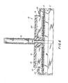
- Terminator 10 includes circuit board 11 sandwiched between first dielectric housing 12 and second dielectric housing 13.
- Circuit board 11 is preferably made from copper clad glass fiber base epoxy resin.
- Dielectric housing 12 is preferably made from unfilled polycarbonate with a flammability rating of 94V-O.
- Dielectric housing 13 is preferably made from a thermoplastic material with a flammability rating of 94V-O.
- Circuit board 11 has a first side 30 and a second side 31, and a plurality of through holes 32. Signal leads 33 are in electrical contact with through holes 32. A plurality of serpent terminals 34 are mounted on first side 30 of circuit board 11. A first contact end of each terminal 34 is mounted in, and is in electrical contact with, a respective hole 32.
- Terminals 34 extend substantially perpendicularly from circuit board 11 substantially parallel to one another.
- resistor networks 35 each equivalent to six resistors, are each mounted on circuit board 11 in electrical contact with twelve of the holes 32.
- Resistor networks 35 together with signal leads 33, present selected resistances between the various terminals 34. These resistances can be selected, by choosing resistor networks 35 and the arrangement of signal leads 33, to create a terminator 10 which will "tell" a computer, with an input/output port of which it is mated, that there is no device in the port, that it should shut down if the particular port in question is accessed, or that it should turn on, or any other "message" of which one skilled in the art might conceive.
- Other types of resistor networks or individual resistors or other types of impedance elements could also be used.
- First dielectric housing 12 has a plurality of terminal receiving channels 14, one for each terminal 34.
- Second dielectric housing 13 covers resistor networks 35 and signal leads 33, and has ventilation openings 15 for dissipation of the heat produced by resistor networks 35. Housings 12, 13 and circuit board 11 are held together by four self-tapping screws 20.
- a jack screw 16 is provided to fix terminator 10 to the connector to which it is mated.
- Jack screw 16 knurled to provide a frictional surface for twisting, is attached to second housing 13 through hole 36 by a C-clip 37, which allows jack screw 16 to rotate while preventing its longitudinal withdrawal from housing 13.
- Jack screw 16 passes through holes 38 in circuit board 11 and first housing 12 for engagement with a threaded hole in the mating connector.
- a threaded insert is provided in hole 39 in first housing 12 to receive a screw, if any, from the mating connector.
- resistor networks 35 in conjunction with signal leads 33 on a circuit board 11 mounted parallel to the mating face of terminator 10 as described above, it is thereby possible to create a terminator which is much more compact than those previously known, and which will project less from the device to which it is mated.
Landscapes
- Engineering & Computer Science (AREA)
- Microelectronics & Electronic Packaging (AREA)
- Details Of Connecting Devices For Male And Female Coupling (AREA)
- Liquid Developers In Electrophotography (AREA)
- Amplifiers (AREA)
- Electrical Discharge Machining, Electrochemical Machining, And Combined Machining (AREA)
- Coupling Device And Connection With Printed Circuit (AREA)
- Cable Accessories (AREA)
- Insulated Conductors (AREA)
Priority Applications (1)
| Application Number | Priority Date | Filing Date | Title |
|---|---|---|---|
| AT86303198T ATE64241T1 (de) | 1985-04-29 | 1986-04-28 | Elektrische endstueckvorrichtung. |
Applications Claiming Priority (2)
| Application Number | Priority Date | Filing Date | Title |
|---|---|---|---|
| US72791885A | 1985-04-29 | 1985-04-29 | |
| US727918 | 1985-04-29 |
Publications (3)
| Publication Number | Publication Date |
|---|---|
| EP0200516A2 true EP0200516A2 (de) | 1986-11-05 |
| EP0200516A3 EP0200516A3 (en) | 1989-02-22 |
| EP0200516B1 EP0200516B1 (de) | 1991-06-05 |
Family
ID=24924638
Family Applications (1)
| Application Number | Title | Priority Date | Filing Date |
|---|---|---|---|
| EP86303198A Expired - Lifetime EP0200516B1 (de) | 1985-04-29 | 1986-04-28 | Elektrische Endstückvorrichtung |
Country Status (9)
| Country | Link |
|---|---|
| EP (1) | EP0200516B1 (de) |
| JP (1) | JPS61250980A (de) |
| KR (1) | KR900003181B1 (de) |
| AT (1) | ATE64241T1 (de) |
| AU (1) | AU583618B2 (de) |
| CA (1) | CA1247750A (de) |
| DE (1) | DE3679589D1 (de) |
| HK (1) | HK100491A (de) |
| SG (1) | SG82391G (de) |
Cited By (4)
| Publication number | Priority date | Publication date | Assignee | Title |
|---|---|---|---|---|
| AU583618B2 (en) * | 1985-04-29 | 1989-05-04 | E.I. Du Pont De Nemours And Company | Electrical terminator device |
| EP0907227A3 (de) * | 1997-10-03 | 1999-11-03 | Thomas & Betts Japan,Ltd. | Elektrischer Verbinder für eine Einheit mit elektronischem Bauteil |
| SG2013094396A (en) * | 2013-12-19 | 2015-07-30 | Rockwell Automation Asia Pacific Business Ctr Pte Ltd | Slice-io housing with side ventilation |
| US9864352B2 (en) | 2015-06-01 | 2018-01-09 | Rockwell Automation Asia Pacific Business Ctr. Pte., Ltd. | Slice I/O—field power bus breaker |
Family Cites Families (8)
| Publication number | Priority date | Publication date | Assignee | Title |
|---|---|---|---|---|
| FR1367183A (fr) * | 1962-11-19 | 1964-07-17 | Burndy Corp | Connexions électriques concentrées |
| DE1930856U (de) * | 1965-08-31 | 1966-01-13 | Licentia Gmbh | Steckbares schaltungselement. |
| GB1397249A (en) * | 1971-12-30 | 1975-06-11 | Lucas Electrical Co Ltd | Electrical connector arrangement |
| JPS5933686U (ja) * | 1982-08-27 | 1984-03-01 | 富士通株式会社 | 抵抗付コネクタ |
| JPS5949378U (ja) * | 1982-09-25 | 1984-04-02 | 株式会社東芝 | コネクタ |
| JPS59165680U (ja) * | 1983-04-22 | 1984-11-06 | 矢崎総業株式会社 | ダイオ−ド及びヒユ−ズ付コネクタ |
| EP0130844B2 (de) * | 1983-07-05 | 1997-09-03 | Sumitomo Wiring Systems, Ltd. | Zwischenverbindungseinrichtung für Kabelbäume |
| KR900003181B1 (ko) * | 1985-04-29 | 1990-05-09 | 이 아이 듀우판 디 네모아 앤드 캄파니 | 전기 종단 장치(terminator device) |
-
1986
- 1986-04-28 KR KR1019860003265A patent/KR900003181B1/ko not_active Expired
- 1986-04-28 JP JP61097029A patent/JPS61250980A/ja active Granted
- 1986-04-28 AT AT86303198T patent/ATE64241T1/de not_active IP Right Cessation
- 1986-04-28 DE DE8686303198T patent/DE3679589D1/de not_active Expired - Lifetime
- 1986-04-28 EP EP86303198A patent/EP0200516B1/de not_active Expired - Lifetime
- 1986-04-29 AU AU56880/86A patent/AU583618B2/en not_active Ceased
- 1986-04-29 CA CA000507840A patent/CA1247750A/en not_active Expired
-
1991
- 1991-10-08 SG SG823/91A patent/SG82391G/en unknown
- 1991-12-12 HK HK1004/91A patent/HK100491A/en not_active IP Right Cessation
Cited By (6)
| Publication number | Priority date | Publication date | Assignee | Title |
|---|---|---|---|---|
| AU583618B2 (en) * | 1985-04-29 | 1989-05-04 | E.I. Du Pont De Nemours And Company | Electrical terminator device |
| EP0907227A3 (de) * | 1997-10-03 | 1999-11-03 | Thomas & Betts Japan,Ltd. | Elektrischer Verbinder für eine Einheit mit elektronischem Bauteil |
| US6379189B2 (en) * | 1997-10-03 | 2002-04-30 | Thomas & Betts Japan, Ltd. | Connector |
| SG2013094396A (en) * | 2013-12-19 | 2015-07-30 | Rockwell Automation Asia Pacific Business Ctr Pte Ltd | Slice-io housing with side ventilation |
| US9420719B2 (en) | 2013-12-19 | 2016-08-16 | Rockwell Automation Asia Pacific Business Ctr. Pte., Ltd. | Slice-IO housing with side ventilation |
| US9864352B2 (en) | 2015-06-01 | 2018-01-09 | Rockwell Automation Asia Pacific Business Ctr. Pte., Ltd. | Slice I/O—field power bus breaker |
Also Published As
| Publication number | Publication date |
|---|---|
| JPS61250980A (ja) | 1986-11-08 |
| AU583618B2 (en) | 1989-05-04 |
| EP0200516B1 (de) | 1991-06-05 |
| KR900003181B1 (ko) | 1990-05-09 |
| KR860008630A (ko) | 1986-11-17 |
| SG82391G (en) | 1991-11-22 |
| AU5688086A (en) | 1987-11-05 |
| EP0200516A3 (en) | 1989-02-22 |
| CA1247750A (en) | 1988-12-28 |
| JPH0578915B2 (de) | 1993-10-29 |
| ATE64241T1 (de) | 1991-06-15 |
| DE3679589D1 (de) | 1991-07-11 |
| HK100491A (en) | 1991-12-20 |
Similar Documents
| Publication | Publication Date | Title |
|---|---|---|
| US4881902A (en) | Electrical terminator device | |
| US4857002A (en) | Terminator assembly for interconnecting computer devices | |
| US5040993A (en) | Interchangeable adapter module for electronic devices | |
| EP0175426B1 (de) | Adapterstecker für den Übergang zwischen zwei Masssystemen unter Verwendung einer gedruckten Schaltung | |
| US4971563A (en) | Modular backplane assemblies for computers | |
| US6948983B1 (en) | Slim USB male connector with anti-disorientation design | |
| US5173063A (en) | Receptacle connector having protected power contacts | |
| US5495584A (en) | SCSI bus concatenator/splitter | |
| US5214567A (en) | Modular peripheral platform having two disk drives and one electrical connector | |
| US5330370A (en) | Multiple-interface selection system for computer peripherals | |
| US5293636A (en) | Module for insertion into a multi-module system having electronic keying for preventing power to improperly connected modules with improperly configured diode connections | |
| US5518418A (en) | SCSI ID connector assembly | |
| US4335272A (en) | Breakaway circuit board with flexible coupling | |
| DE69527199D1 (de) | Programmierbarer kabeladapter | |
| US4954089A (en) | Terminator assembly for interconnecting computer devices | |
| US6945820B1 (en) | Electrical connect having integrated over current protector | |
| US4398779A (en) | Keying apparatus for interconnecting electrical components | |
| EP0467595B1 (de) | Personalcomputer mit Verbinderanordnung, welcher eine Verriegelungsvorrichtung aufweist | |
| US4235496A (en) | Circuit board and card interconnection system | |
| US5692917A (en) | Computer hardware insert device for software authorization | |
| EP0443492B1 (de) | Steckverbinder mit geschützten Leistungskontakten | |
| US4272141A (en) | Electronic card cage interfacing assembly | |
| EP0200516B1 (de) | Elektrische Endstückvorrichtung | |
| US6480925B1 (en) | Compact and versatile SCA to SCSI bus adapter | |
| US5436800A (en) | Zero impact module ejection system |
Legal Events
| Date | Code | Title | Description |
|---|---|---|---|
| PUAI | Public reference made under article 153(3) epc to a published international application that has entered the european phase |
Free format text: ORIGINAL CODE: 0009012 |
|
| AK | Designated contracting states |
Kind code of ref document: A2 Designated state(s): AT BE CH DE FR GB IT LI LU NL SE |
|
| PUAL | Search report despatched |
Free format text: ORIGINAL CODE: 0009013 |
|
| AK | Designated contracting states |
Kind code of ref document: A3 Designated state(s): AT BE CH DE FR GB IT LI LU NL SE |
|
| 17P | Request for examination filed |
Effective date: 19890621 |
|
| 17Q | First examination report despatched |
Effective date: 19891220 |
|
| GRAA | (expected) grant |
Free format text: ORIGINAL CODE: 0009210 |
|
| AK | Designated contracting states |
Kind code of ref document: B1 Designated state(s): AT BE CH DE FR GB IT LI LU NL SE |
|
| REF | Corresponds to: |
Ref document number: 64241 Country of ref document: AT Date of ref document: 19910615 Kind code of ref document: T |
|
| ITF | It: translation for a ep patent filed | ||
| ET | Fr: translation filed | ||
| REF | Corresponds to: |
Ref document number: 3679589 Country of ref document: DE Date of ref document: 19910711 |
|
| PLBE | No opposition filed within time limit |
Free format text: ORIGINAL CODE: 0009261 |
|
| STAA | Information on the status of an ep patent application or granted ep patent |
Free format text: STATUS: NO OPPOSITION FILED WITHIN TIME LIMIT |
|
| 26N | No opposition filed | ||
| PGFP | Annual fee paid to national office [announced via postgrant information from national office to epo] |
Ref country code: SE Payment date: 19930301 Year of fee payment: 8 |
|
| PGFP | Annual fee paid to national office [announced via postgrant information from national office to epo] |
Ref country code: CH Payment date: 19930302 Year of fee payment: 8 |
|
| PGFP | Annual fee paid to national office [announced via postgrant information from national office to epo] |
Ref country code: BE Payment date: 19930401 Year of fee payment: 8 |
|
| PGFP | Annual fee paid to national office [announced via postgrant information from national office to epo] |
Ref country code: LU Payment date: 19930406 Year of fee payment: 8 |
|
| PGFP | Annual fee paid to national office [announced via postgrant information from national office to epo] |
Ref country code: AT Payment date: 19930413 Year of fee payment: 8 |
|
| PGFP | Annual fee paid to national office [announced via postgrant information from national office to epo] |
Ref country code: NL Payment date: 19930430 Year of fee payment: 8 |
|
| EPTA | Lu: last paid annual fee | ||
| PG25 | Lapsed in a contracting state [announced via postgrant information from national office to epo] |
Ref country code: LU Free format text: LAPSE BECAUSE OF NON-PAYMENT OF DUE FEES Effective date: 19940428 Ref country code: AT Effective date: 19940428 |
|
| PG25 | Lapsed in a contracting state [announced via postgrant information from national office to epo] |
Ref country code: SE Effective date: 19940429 |
|
| PG25 | Lapsed in a contracting state [announced via postgrant information from national office to epo] |
Ref country code: LI Effective date: 19940430 Ref country code: CH Effective date: 19940430 Ref country code: BE Effective date: 19940430 |
|
| BERE | Be: lapsed |
Owner name: E.I. DU PONT DE NEMOURS AND CY Effective date: 19940430 |
|
| PG25 | Lapsed in a contracting state [announced via postgrant information from national office to epo] |
Ref country code: NL Effective date: 19941101 |
|
| NLV4 | Nl: lapsed or anulled due to non-payment of the annual fee | ||
| REG | Reference to a national code |
Ref country code: CH Ref legal event code: PL |
|
| EUG | Se: european patent has lapsed |
Ref document number: 86303198.5 Effective date: 19941110 |
|
| REG | Reference to a national code |
Ref country code: GB Ref legal event code: 732E |
|
| REG | Reference to a national code |
Ref country code: FR Ref legal event code: TP |
|
| REG | Reference to a national code |
Ref country code: GB Ref legal event code: IF02 |
|
| PGFP | Annual fee paid to national office [announced via postgrant information from national office to epo] |
Ref country code: GB Payment date: 20020315 Year of fee payment: 17 |
|
| PGFP | Annual fee paid to national office [announced via postgrant information from national office to epo] |
Ref country code: FR Payment date: 20020404 Year of fee payment: 17 |
|
| PGFP | Annual fee paid to national office [announced via postgrant information from national office to epo] |
Ref country code: DE Payment date: 20020430 Year of fee payment: 17 |
|
| PG25 | Lapsed in a contracting state [announced via postgrant information from national office to epo] |
Ref country code: GB Free format text: LAPSE BECAUSE OF NON-PAYMENT OF DUE FEES Effective date: 20030428 |
|
| PG25 | Lapsed in a contracting state [announced via postgrant information from national office to epo] |
Ref country code: DE Free format text: LAPSE BECAUSE OF NON-PAYMENT OF DUE FEES Effective date: 20031101 |
|
| GBPC | Gb: european patent ceased through non-payment of renewal fee | ||
| PG25 | Lapsed in a contracting state [announced via postgrant information from national office to epo] |
Ref country code: FR Free format text: LAPSE BECAUSE OF NON-PAYMENT OF DUE FEES Effective date: 20031231 |
|
| REG | Reference to a national code |
Ref country code: FR Ref legal event code: ST |
|
| PG25 | Lapsed in a contracting state [announced via postgrant information from national office to epo] |
Ref country code: IT Free format text: LAPSE BECAUSE OF NON-PAYMENT OF DUE FEES;WARNING: LAPSES OF ITALIAN PATENTS WITH EFFECTIVE DATE BEFORE 2007 MAY HAVE OCCURRED AT ANY TIME BEFORE 2007. THE CORRECT EFFECTIVE DATE MAY BE DIFFERENT FROM THE ONE RECORDED. Effective date: 20050428 |