EP0200977B1 - Démodulateur numérique - Google Patents
Démodulateur numérique Download PDFInfo
- Publication number
- EP0200977B1 EP0200977B1 EP86105467A EP86105467A EP0200977B1 EP 0200977 B1 EP0200977 B1 EP 0200977B1 EP 86105467 A EP86105467 A EP 86105467A EP 86105467 A EP86105467 A EP 86105467A EP 0200977 B1 EP0200977 B1 EP 0200977B1
- Authority
- EP
- European Patent Office
- Prior art keywords
- signal
- output
- pass filter
- low
- frequency
- Prior art date
- Legal status (The legal status is an assumption and is not a legal conclusion. Google has not performed a legal analysis and makes no representation as to the accuracy of the status listed.)
- Expired - Lifetime
Links
Images

Classifications
-
- H—ELECTRICITY
- H03—ELECTRONIC CIRCUITRY
- H03D—DEMODULATION OR TRANSFERENCE OF MODULATION FROM ONE CARRIER TO ANOTHER
- H03D1/00—Demodulation of amplitude-modulated oscillations
- H03D1/22—Homodyne or synchrodyne circuits
- H03D1/24—Homodyne or synchrodyne circuits for demodulation of signals wherein one sideband or the carrier has been wholly or partially suppressed
-
- G—PHYSICS
- G08—SIGNALLING
- G08G—TRAFFIC CONTROL SYSTEMS
- G08G1/00—Traffic control systems for road vehicles
- G08G1/09—Arrangements for giving variable traffic instructions
- G08G1/091—Traffic information broadcasting
- G08G1/094—Hardware aspects; Signal processing or signal properties, e.g. frequency bands
-
- H—ELECTRICITY
- H04—ELECTRIC COMMUNICATION TECHNIQUE
- H04H—BROADCAST COMMUNICATION
- H04H40/00—Arrangements specially adapted for receiving broadcast information
- H04H40/18—Arrangements characterised by circuits or components specially adapted for receiving
-
- G—PHYSICS
- G08—SIGNALLING
- G08G—TRAFFIC CONTROL SYSTEMS
- G08G1/00—Traffic control systems for road vehicles
- G08G1/09—Arrangements for giving variable traffic instructions
- G08G1/091—Traffic information broadcasting
-
- H—ELECTRICITY
- H04—ELECTRIC COMMUNICATION TECHNIQUE
- H04H—BROADCAST COMMUNICATION
- H04H2201/00—Aspects of broadcast communication
- H04H2201/10—Aspects of broadcast communication characterised by the type of broadcast system
- H04H2201/13—Aspects of broadcast communication characterised by the type of broadcast system radio data system/radio broadcast data system [RDS/RBDS]
Definitions
- the invention relates to a digital demodulator for demodulating input signals which have a first amplitude-modulated signal (AM signal) containing a high-frequency carrier and / or a second amplitude-modulated signal (AM signal) with suppressed carrier, the two carriers having the same frequency and around 90 ° are out of phase, the type specified in the preamble of claim 1.
- AM signal first amplitude-modulated signal
- AM signal second amplitude-modulated signal
- Such digital demodulators are required for car radios with and without traffic broadcasting (VRF) identification, in which so-called RDS; (radio data system) - information must be decoded.
- VRF traffic broadcasting
- RDS radio data system
- the VRF identifier is a switching information item that is sent out by so-called VRF transmitters. This switching information is contained in an amplitude-modulated 57 kHz carrier, which is emitted as an additive part of a so-called MPX signal by certain radio stations.
- the RDS information relates to transmitter identification, program type, alternative transmission frequencies etc.
- a 1.1875 kHz square wave is phase-modulated on the transmitter side with a bit sequence that characterizes the RDS information, the change in the value of a bit from 0 to 1 Phase of the square wave shifts by 180 ° and vice versa.
- the resulting RDS signal is modulated onto a 57 kHz carrier (amplitude modulation) and phase-shifted by 90 ° compared to a so-called VRF carrier, whose carrier frequency is also 57 kHz.
- the 57 kHz carrier is suppressed in the modulated signal and the resulting signal is added to an MPX signal, which is then processed into a frequency-modulated transmission signal.
- the FM-demodulated signal i.e. the recovered MPX signal
- the digital demodulator which recovers both the VRF identifier and the RDS information - if available - from this input signal.
- the analog-to-digital converter hereinafter referred to as A / D converter
- a / D converter is designed as a delta modulator, to which the input signal is fed.
- the delta-modulated input signal is mixed with an auxiliary signal and fed to a low-pass filter circuit.
- the mixer consists of two exclusive-OR elements, hereinafter referred to as EX / OR elements, the auxiliary signal supplied to one input of the one EX / OR element being phase-shifted by 90 '.
- the low-pass filter circuit here consists of two counters which integrate the input values over a counting period corresponding to three times the period of the carrier.
- the demodulated AM signal that is to say the modulation signal or RDS signal
- a signal shifted by 90 ' the most significant bit of which directly forms the synchronization signal for the frequency generator, can be removed from the second counter.
- the auxiliary signal is multiplied in the mixer by the signal of the modulation signal, that is to say the RDS signal, and is restricted to the processing path which is connected upstream of the second counter.
- this digital demodulator can also snap onto the VRF carrier, the locking of its PLL onto the carrier-free signal with the RDS information or onto the VRF carrier being purely random. however, if the demodulator is locked onto the carrier-free signal, the VRF identifier cannot be demodulated and occurs as a fault.
- the invention has for its object to provide a demodulator of the type mentioned, which demodulates both an AM signal with an existing carrier and an AM signal with a suppressed carrier and can be implemented as a largely monolithically integrable circuit.
- the demodulator according to the invention has the advantage that its PLL always snaps onto the VRF carrier when it is present. Only when there is no VRF carrier does the PLL lock onto the AM signal with the carrier suppressed. In all cases, the RDS information is recovered largely without interference. If the VRF carrier is present, the VRF identifier is also reliably determined.
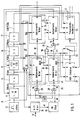
- the digital demodulator shown in the block diagram in FIG. 1 serves to demodulate input signals which have a first amplitude-modulated signal containing a high-frequency carrier, hereinafter referred to as AM signal, and / or a second AM signal with suppressed carrier, the two carriers are of the same frequency and are out of phase by 90 * .
- the first AM signal contains the so-called VRF signal as a modulation signal
- the second AM signal contains the so-called RDS signal as a modulation signal.
- the frequency of the VRF carrier like the frequency of the suppressed RDS carrier, is 57 kHz.
- Both AM signals are contained as an additive part in a so-called MPX signal, which is received by the receiver as a frequency-modulated transmission signal.
- the MPX signal lacks the first AM signal and only the second AM signal with the carrier suppressed is present.
- the additive part of the MPX signal is fed to the input 10 of the demodulator via a bandpass filter.
- the demodulator has a frequency generator 11 which consists of a 4 MHz square wave generator 12 and a plurality of frequency dividers connected in series.
- the frequency divider 13 directly connected to the square wave generator 12 has a controllable divider ratio, which depending on the input signal at its control input can be switched from 17 to 18 and vice versa.
- a 228 kHz rectangular pulse train is thus available on average.
- the subsequent frequency divider 14 has the constant divider ratio 4, so that a 57 kHz square wave pulse sequence can be removed at its output.
- the subsequent frequency divider 15 in turn has a controllable divider ratio, which can be switched from 12 to 11 or 13 and vice versa, depending on the control signal.
- a 4.75 kHz rectangular pulse train can be removed.
- the two subsequent frequency dividers 16 and 17 each have the divider ratio 2, so that a 2,375 kHz or 1.1875 kHz square pulse sequence is present at their outputs.
- a / D converter 18 8-bit analog-to-digital converter 18, hereinafter referred to as A / D converter 18, is connected, which is clocked with the 228 kHz rectangular pulse train.
- the digital values are fed to a serial shift register 19.
- the digital values are supplied bit by bit to a mixer 20 from the shift register 19, with eight further zeros being added after every 8 bit values of the A / D converter 18, so that a 16 bit word is present in series at the input of the mixer 20.
- the mixer 20 is also supplied with a carrier-frequency auxiliary signal, which is represented here by the 57 kHz rectangular pulse train of the frequency generator 11.
- the mixer 20 is followed by a low-pass filter circuit 21, the output signal of which is separated into sine and cosine components and can be taken off at a first output 22 as the first output signal and at a second output 23 as the second output signal.
- a first low-pass filter 24 is connected to the first output 22 and a second low-pass filter 26 is connected to the second output 23 with the interposition of a multiplier 25.
- the output d of the second low-pass filter 26 is connected to the control input of the first frequency divider 13 with the interposition of logic not shown here.
- the low-pass filter circuit 21 has an output data rate which is an even multiple of the modulation frequency of the second AM signal, ie the frequency. of the RDS signal, and is dimensioned at least equal to four times this modulation frequency and at most equal to the carrier frequency 57 kHz of the first AM signal.
- the output data rate of the low-pass filter circuit 21 is chosen to be 4.75 kHz.
- the output data rate of the two low-pass filters 24, 26 is equal to the modulation frequency of the second AM signal, ie 1.1875 kHz.
- the modulation signal contained in the first AM signal, ie the VRF signal can be removed.
- the mixer 20 has two exclusive-OR elements 28, 29, hereinafter referred to as EX / OR elements 28, 29 for short.
- EX / OR elements 28, 29 One input each of the two EXJOR elements 28, 29 is connected to the output of the serial shift register 19.
- the other output of the EX / OR gate 28 is occupied with the 57 kHz square pulse sequence and the other input of the EX / OR gate 29 with the rectangular pulse sequence shifted by 90 ', for which purpose here in the connecting line from the output of the frequency divider 14 to the input of the EX / OR gate 29, a 90 'phase shifter 30 is shown.
- this phase shifter will not be found, since usually the frequency dividers are constructed in such a way that with a divider ratio of 1: 4, all four phases are therefore 0, ⁇ 90 ', 180' available.
- the low-pass filter circuit 21 has two serial adders 31, 32, the input a of the first adder 31 being connected to the output of the EX / OR gate 28 and the input a of the second adder 32 being connected to the output of the EX / OR gate 29 .
- the further inputs b and c of the two adders 31, 32 are connected to a clock adapter 37, which in turn is connected to some outputs of the frequency generator 11.
- the two low-pass filters 24, 26 are also formed in FIG. 1 as serial adders 33, 34, the input a of the third adder 33 being connected directly to the output d of the first adder 31, while the input a of the fourth adder 34 is connected via the Multiplier 25 is connected to the output d of the second adder 32.
- the multiplier 25 here has an EX / OR gate 35 and a NOR gate 36.
- the output of the EX / OR gate 35 is connected to the input a of the fourth Adding unit 34 connected.
- One input of the EX / OR gate 35 is at the output d of the second adder 32 and the other input is at the output of the NOR gate 36.
- the two inputs of the NOR gate 36 one is at the output f of the VRF -Detector 27 and the other at a partial output of the first adder 31, which carries the most significant bit (MSB) of the first output signal.
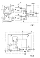
- the structure of the clock matching circuit 37 is shown in detail in FIG. 2. For the sake of clarity, the frequency assignment of the connections I-V and the connections of the outputs VI-IX of the clock matching circuit 37 to other components are listed in FIG. 1 in FIG. 2.
- the logical combination of the logic elements, such as D flip-flops 90, 91, 92, 93, NOR gate 94, AND gate 95 and OR gate 96 with one another and with the inputs IV of the clock matching circuit 37 ensures that at the Output VI a bundle of sixteen 4 MHz pulses with a repetition frequency of 228 kHz, at output VIII an identical bundle of sixteen pulses with a repetition frequency of 4.75 kHz, at output VII an inverted 4.75 kHz square-wave pulse train with a duty cycle of 1:48 and at the output IX there is an inverted 1.1875 kHz square pulse train with a duty cycle of 1: 4.
- the D flip-flops 90, 91 generate a 228 kHz square pulse sequence with a test ratio of 1 17.5, which is linked to the 228 kHz square pulse sequence by the NOR gate 94.
- the series connection of the D flip-flops 92, 93 generates a 4.75 kHz square pulse sequence with a pulse duty factor of 1:48, which is linked to the output of the NOR gate 94 through the AND gate 95.
- the inverted rectangular pulse train at output VII is taken from the Q output of the D flip-flop 95, while the inverted rectangular pulse train at output IX is obtained by ORing the 2.375 kHz and 1.1875 kHz rectangular pulse trains in OR gate 96 .
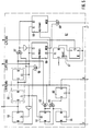
- the structure of the adders 31-34 is identical and shown in Fig. 4.
- the adders 31 and 32 differ from the adders 33 and 34 only in the clock assignment of the inputs b and c, as described above.
- Each adder 31-34 has a serial 1-bit adder 40 and a 16-bit serial shift register 41 connected downstream thereof, the output of which is fed back to the input of the adder 40 via an AND gate 42 which acts as a gate element.
- the other input of the AND gate 42 is connected to the input c of the adder 31-34.
- the clock inputs 01 of the adder 40 and the shift register 41 are connected to the input b of the respective adder 31-34.
- the fine structure of the 1-bit adder 40 is readily apparent from FIG. 4.
- the 16-bit word present at the input a is added bit by bit to the content of the shift register 41.
- this goes over twelve periods of 57 kHz (one period of 4.75 kHz), i. H. 48 16-bit words or sampies from mixer 20 are added up (see pulse bundle at output VI of the key matching circuit 37).
- the input c of the adders 31, 32 is logic 0 (cf. 4.75 kHz square-wave pulse sequence with asymmetrical duty cycle at the output VII of the clock matching circuit 37), so that only the bit values appearing at the input a are in the shift register 41 can be registered.
- the shift register 41 is thus reset.
- the bit values appearing at the output d and previously stored in the shift register 41 are each transferred to the adders 33, 34.
- the input b of these adders 33, 34 receives a bundle of 16 pulses from the output VIII of the clock matching circuit 37, but only if the input c of the adders 31, 32 is zero.
- the adder units 33 and 34 four of the 16 bit words adopted by the adder units 31 and 32 are first added up. After every fourth of these additions - that is to say at a rate of 1.1875 kHz - the input c of the two adders 33, 34 becomes zero for a 4.75 kHz period (cf. 1.1875 kHz square-wave pulse sequence with asymmetrical pulse duty factor at the output IX the clock matching circuit 37).
- the shift registers 41 of the two adders 33, 34 are evaluated.
- the PLL of the demodulator should snap onto its carrier and if the VRF signal is missing, it must be able to snap onto the second AM signal with the carrier suppressed.
- the 16-bit output signal of the adder 32 is multiplied by the signum of the 16-bit output signal of the adder 31. This signum is represented by the MSB of the 16-bit output signal, so that the one input of the EX / OR gate 35 is connected via the NOR gate 36 to the partial output of the adder 31 carrying this most significant bit. If the VRF signal is present, this signal multiplication must be suppressed so that the PLL snaps onto the VRF carrier.
- the VRF detector 27 takes on this task.
- the VRF detector 27 works in such a way that it outputs the output signals of the low-pass filter circuit 21, here. that is, the output signals of the two adders 31 and 32 are checked for constancy of their polarity and then emits an output signal which is characteristic of the presence of the VRF signal if at least one of the two output signals of the low-pass filter circuit 21 has constant polarity over a predetermined period of time.
- the two detector inputs a and b are each connected to the outputs of the adder units 31, 32, specifically with the partial output which carries the most significant bit.
- a D flip-flop 43 or 44, a NAND gate 45 or 46 and a 4-bit counter 47 or 48 are assigned to each detector input a or b, the D input of the D flip-flop in each case 43 and 44 and one input of the NAND gate 45 and 46 with the detector input a and b, the other input of the NAND gate 45 and 46 with the Q input of the D flip-flop 43 and 44 and the output of the D flip-flop 45 or 46 is connected to the negated reset input of the 4-bit counter 47 or 48.
- the clock input of the two 4-bit counters 47, 48 is connected to the 1.1875 kHz output of the frequency generator 11 via a NOR gate 49 and 50, while the other input of the NOR gate 49, 50 is connected to the MSB Output of the assigned 4-bit counter 47 or 48 is connected.
- the MSB outputs of the two 4-bit counters 47, 48 are connected via a further NOR gate 51 to the up / down counter input of an 8-bit up / down counter 52, at the clock input CI of which a rectangular pulse sequence of approximately 500 Hz lies, the z. B. can be obtained from the 1.1875 kHz rectangular pulse train by appropriate frequency division (z. B. by the divider 2).
- the MSB output of the up / down counter 52 forms the output f of the VRF detector gate 27, which is connected to the multiplier 25.
- an output signal of the adders 31 and 32 has a constant sign, the output signal of the adder 32 being constant when the PLL is locked onto the second AM signal with the carrier suppressed.
- the sign is constant, there are no edges at detector inputs a and b: If the signs are not constant, however, the edges at inputs a and b reset the 4-bit counters 47, 48. If the sign of one of the output signals is constant, at least one counter 47, 48 reaches the number 8 and remains there because its clock frequency of 1.1875 kHz is switched off via the MSB.
- the output signal of the VRF detector 27 is simultaneously supplied as a control signal to an electronic switch 53, the output of which is connected to the input E of a circuit arrangement for demodulating the phase modulation contained in the modulation signal of the AM signal with suppressed carrier.
- This circuit arrangement is referred to below as an RDS or phase demolator 54.
- the two inputs of the changeover switch 53 are connected to the two outputs of the low-pass filter circuit 21, and expediently to the partial output carrying the most significant bit.
- the changeover switch 53 is controlled so that when the VRF signal is present (output signal of the VRF detector 27 logic 1), the changeover switch assumes the position shown in FIG.
- phase demodulator 54 1, in which the most significant bit of the 16 bit output signal of the second adder 32 arrives is the input E of the Pasdemodulators 54, four times per 1.1875 kHz period. If there is no VRF signal, the output of the switch 53 is switched to the other input, so that the most significant bit of the output signal of the first adder 31 now reaches the phase demodulator 54 in the same way.
- the structure and mode of operation of the phase demodulator 54 which is also described in the document DE-A-3510562- (published on September 25, 1986), will be discussed below.
- the FM signal after FM demodulation of the received signal as an additive part of the MPX signal after bandpass filtering at input 10 of the demodulator can be described with with the modulation signals
- VRF identifier and RDS information are contained in the MPX signal, A and R assume the values given above. If the VRF identifier or the RDS information is missing, A and R are zero in each case.
- This input signal is converted into 8-bit samples in the A / D converter 18 with a clock frequency of 228 kHz and read into the shift register 19.
- the samples converted into a 16-bit word when read out from the shift register 19 are mutually separated by 90 'in the mixer 20 phase-shifted 57 kHz rectangular pulse trains are multiplied, the signal path being divided into a sine and a cosine path.
- This multiplication corresponds to an evaluation of the four 228 kHz samples per 57 kHz period in the sine path with + 1, + 1, - 1, - and in the cosine path with + 1, - 1, - 1, + 1.
- the samples of a total of twelve 57 kHz periods ie a total of 48 samples, are added up separately for each signal path.
- the GI. (1) assumed signal would result in the addition of the samples in a 57 kHz period for the sine path in the first adder 31 and for the cosine path in the second adder 32
- the output variables of the two adders 31, 32 are then approximately twelve times as large, corresponding to the summation over twelve 57 kHz periods.
- each of the two adders 33 and 34 four output variables or output signals of the adders 31, 32 are added. If the PLL is locked onto the 57 kHz VRF carrier, the phase shift ⁇ p is approximately zero. How to get out of the GI. (4) and (5) can be seen, is therefore at the output d of the third adder 33, the modulation signal A, so the VRF signal, and at the output d of the fourth adder 34, the VRF signal multiplied by the sine of the phase error, as a result of integration over a 1.1875 kHz period the RDS component of the signal becomes zero on average.
- the output signal of the adder 34 is fed to the frequency generator 11 as a phase correction signal, as a result of which the divider ratio of the first frequency divider 13 is changed briefly and the phase error ⁇ is thereby further reduced.
- the RDS signal (R) appears at the output of the second adder 32.
- the four output values at the output of the second adder 32 are multiplied by the signum (sign) of the output values at the output of the first adder 31 in every 4.75 kHz period and by a 1.1875 kHz Period added up. If the PLL is locked onto the carrier-free AM signal, the phase shift is ⁇ ⁇ - 90 °.
- the output signal of the first adder 31 represents the RDS signal (R), while zero occurs at the output d of the third adder 33, since the integration of the four output values of the first adder 31 via a 1, 1875 kHz period results in zero on average.
- the electronic Since - as mentioned - the RDS signal, depending on whether the VRF signal is present in the MPX signal or not, is present once at the output of the second adder 32 and once at the output of the first adder 31, the electronic becomes - as described Switch 53 controlled by the VRF detector 27 so that the RDS signal always appears at the output of the electronic switch 53 and is therefore at the input E of the RDS or pasmodule 24. It is sufficient - as here - of the 16 bit word of the RDS signal, only the most significant bit (MSB) is to be fed to the input E of the phase demodulator 54.
- MSB most significant bit
- phase demodulator 54 The structure of the phase demodulator 54 is shown in detail in FIG. 5. It should also be noted that the structure and mode of operation of the phase demodulator 54 are described in detail in document DE-A-3510562, so that the phase demodulator 54 is only briefly dealt with here for the sake of completeness.
- the task of the phase demodulator 54 is to recover the bit sequence contained in the RDS signal, the so-called RDS information.
- the input of a 2-bit shift register 55 clocked with the 2.375 kHz square-wave pulse sequence and the input of a 1-bit shift register 56 clocked with the inverted 2.375 kHz square-wave pulse sequence are connected to input E.
- the two parallel bit outputs of the 2-bit shift register 55 are connected to a first comparator 57 and the one bit output of the 2-bit shift register 55 and the output of the 1-bit shift register 56 to a comparator 58.
- Two up / down counters 59, 60 are connected to the output of the first comparator 57 in such a way that an inequality signal at the comparator output which is characteristic of the inequality of the comparator input signals is given to the first counter 59 and an equality signal at the comparator output which is characteristic of the equality of the comparator input signals is at the second Counter 60 is supplied.
- the two counters 59, 60 are designed such that the respective output signal of the comparator 57 increments the first counter 59 depending on the output signal of the second comparator 58 and the second counter 60 depending on the current polarity of the 1.1875 kHz square-wave pulse sequence decremented.
- a synchronization circuit 61 is connected to the outputs of the two counters 59, 60, the outputs of which form the 2-bit phase correction output r / r 'of the phase demodulator 54, which is connected to the control input of the third frequency divider 15 with a controllable division ratio.
- the synchronization circuit 61 generates a time-limited control signal for switching the divider ratio of the frequency divider 15 from the output signals of the counters 59, 60.
- a third comparator 62 is connected on the input side, on the one hand, to a bit output of the 2-bit shift register 55 and, on the other hand, is assigned the 1.1875 kHz square-wave pulse sequence.
- the series connection of two D-flip-flops 63, 64 is connected to the output of the third comparator 62, of which the first D-flip-flop 63 is clocked at 2.375 kHz and the second D-flip-flop 64 is clocked at 1.1875 kHz becomes.
- the D input and the Q output of the first D flip-flop 63 are connected to a further comparator 65, to the output of which a D flip-flop 66 is connected, which is clocked at 1.1875 kHz.
- the bit sequence T of the RDS information can be removed at the Q output of the D flip-flop 63, that is to say at the output t of the phase demodulator 54.
- a quality statement Q about the correctness of the bit sequence present at the D output can be removed.
- the comparators 57, 58, 62 and 65 are all designed here as exclusive-OR gates.
- the MSB of a 16-bit word is at the input E of the phase demodulator 54 at the output of the first or second adder 31 or 32, that is to say four bits within an RDS period of 1.1875 kHz. These bits represent samples of the RDS signal and are out of phase with each other by a quarter of the RDS period. Each sample lies approximately in a zero or an extreme value of the RDS signal.
- the clock of the two ski registers reads all even-numbered samples that correspond to the extreme values of the RDS signal into the 2-bit shift register 55 and all odd-numbered samples that correspond to zeros of the RDS signal into the 1-bit shift register 56. Sampling one period of the RDS signal forms one sampling cycle.
- the successive even-numbered samples of all sampling cycles are compared with one another in the comparator 57. If the comparison values are not identical, the intermediate odd sample value is checked in the comparator 58 for parity with the comparison value that follows or precedes the scan sequence.
- the test results of the comparator 58 are added or subtracted in the counter 59 according to their parity, which means that the counter 59 is incremented or decremented by 1 for each clock. From the sum, a synchronization signal is generated by the synchronization circuit 61 via the MSB of the counter 59, which controls the direction of an RDS phase tracking by incremental 1 per 57 kHz period. The frequency of this measure is determined by the carry pulse of counter 59, which resets counter 59 by a quarter of its counting range.
- the carry pulse triggers in a gate 67 of the synchronization circuit 61 a gate pulse of the duration of a 4.75 kHz period in which the synchronization signal of the synchronization circuit 61 is effective.
- the PLL of the phase demodulator 54 can thus snap into place, but is undetermined by 180 '.
- the counter 60 is used to determine whether the two sampling values belong to successive sampling cycles or to the same sampling cycle.
- the bit limit of the RDS information with the RDS signal is correct, the RDS PLL is correctly locked.
- the RDS-PLL is locked out of phase by 180 °.
- the counter 60 is incremented by 1 with each clock.
- the MSB of the counter 60 the direction of the RDS phase correction is inverted via an exclusive-OR gate 68 of the synchronization circuit 61, so that the phase runs away, the stable position changes into a labile one and the PLL can then latch properly.
- the comparator 62 is used to decide twice per RDS period whether the even-numbered sample values, that is to say the extreme values, correspond in polarity to the 1.1875 kHz rectangular pulse sequence men, ie whether the telegram content, ie the current bit of the bit sequence of the RDS switching information is logic 0 or logic 1.
- One of these results is output at the Q output of the D flip-flop 64 as a bit of the RDS switching information.
- the comparison of the two results of an RDS period in the comparator 65 provides the quality statement Q at the output of the D flip-flop 66.
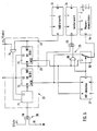
- FIG. 6 shows a modified exemplary embodiment of a demodulator, as described for FIG. 1, in sections.
- This demodulator differs from that in FIG. 1 only with regard to the construction of the mixer 20 and the low-pass filter circuit 21. The same components are therefore provided with the same reference numerals.
- the mixer 20 consists of only one EX / OR gate 70, at one input of which the 57 kHz rectangular pulse train from the output of the frequency divider 14 is connected and the other input of which is connected to the shift register 19 in FIG. 1 is.
- the low-pass filter circuit 21 connected downstream of the mixer 20 represents a serial adder with two memories.
- This serial adder has a serial 1-bit adder 71, which is constructed identically to the 1-bit adder 40 in FIG. 4.
- a series circuit comprising two 16-bit shift registers 72, 73 is connected to the output of the adder 71.
- Each output of a shift register forms an output 22, 23 of the low-pass filter circuit 21, the output of the shift register 72 directly connected to the adder 71 representing the second output 23 and the output of the last shift register 73 in the series connection representing the first output 22 low-pass filter circuit.
- the output of the last shift register 73 in the series circuit is fed back via an AND gate 74 in the same way as in FIG. 4 to the input of the adder 71.
- the other input of the AND gate 74 is at the input c, which is connected to the output VII of the clock matching circuit 37.
- the clock inputs of adder 71 and shift register 72, 73 are connected to the input b, which in turn - as in FIG.
- the inputs b of the adders 31, 32 - is connected to the output VI of the clock matching circuit 37.
- the other components and their electrical connection are the same as in FIG. 1, so that this circuit supplement has not been shown in some cases.
- the adder 33 is connected to the first output 22 of the low-pass filter circuit 21 and the adder 34 is connected to the second output 23, the signum multiplier 25 consisting of the EX / OR Member 35 and the NOR gate 36 is turned on.
- the MSB outputs of the shift registers 72, 73 are connected on the one hand to the inputs of the electronic switch 53 and on the other hand to the inputs of the VRF detector 27.
- the MSB output of the shift register 73 is also connected to one input of the NOR gate 36, the other input of which is in a known manner at the output f of the VRF detector 27.
- the 16-bit samples at the output of the shift register 19 are multiplied in the mixer 20 by the carrier-frequency auxiliary signal, that is to say by the 57 kHz square-wave pulse sequence.
- This multiplication corresponds to an evaluation of the four 228 kHz samples per 57 kHz period with + 1, + 1, - 1, - 1. Divided into a cosine and sine path, this would result in an evaluation in the sine path with 0, + 1, 0, - 1 and in the cosine path with + 1, 0, - 1, 0 mean.
- this demodulator is that the two memories can be made 1 bit smaller because fewer bit values are added up in a 4.75 kHz period (twelve 57 kHz periods).
- the circuit complexity for mixer 20 and low-pass filter circuit 21 is almost halved, since the processing in the sine path and in the cosine path is not carried out in parallel, but alternately.
- This time-division multiplexing of the hardware is particularly interesting when complex feedback or higher-order filters (cascading) are required to increase the low-pass effect.
- FIG. 7 Another exemplary embodiment of the demodulator described here is shown in detail in FIG. 7 in the block diagram.
- the A / D conversion and the mixing of the input signal are reversed here.
- the analog input signal in the mixer 81 is multiplied once by the carrier-frequency auxiliary signal and once by the carrier-frequency auxiliary signal which is out of phase.
- Each mixed product at the output of the mixer 81 is processed separately, first to a low-pass filter 82 or 83, then to an A / D converter 84 or 85, to which the low-pass filter circuit 21 with its two inputs is finally connected.
- the low-pass filter circuit 21 consists of two adders 31 and 32, each assigned to an input.
- the outputs 22, 23 of the low-pass filter circuit 21 are then connected to the identical circuit as in FIG. 1.
- the A / D converters 84, 85 are also clocked as in FIG. 1 by the 228 kHz rectangular pulse train of the frequency generator 11.
- This demodulator has the advantage that interference that is far outside 57 kHz (LF, stereo) is already eliminated before the A / D conversion, so that the A / D converter 84, 85 already has a smaller word length of z. B. 5 or 6 bits instead of 8 bits is sufficient.
- the sampling frequency of the A / D converter 84, 85 can be chosen to be significantly lower, e.g. B. 19 kHz instead of 228 kHz.
Landscapes
- Engineering & Computer Science (AREA)
- Signal Processing (AREA)
- Power Engineering (AREA)
- Multimedia (AREA)
- Physics & Mathematics (AREA)
- General Physics & Mathematics (AREA)
- Digital Transmission Methods That Use Modulated Carrier Waves (AREA)
- Signal Processing For Digital Recording And Reproducing (AREA)
- Stabilization Of Oscillater, Synchronisation, Frequency Synthesizers (AREA)
- Superheterodyne Receivers (AREA)
- Optical Recording Or Reproduction (AREA)
- Amplifiers (AREA)
Claims (10)
Priority Applications (1)
| Application Number | Priority Date | Filing Date | Title |
|---|---|---|---|
| AT86105467T ATE51478T1 (de) | 1985-05-07 | 1986-04-21 | Digitaler demodulator. |
Applications Claiming Priority (2)
| Application Number | Priority Date | Filing Date | Title |
|---|---|---|---|
| DE19853516282 DE3516282A1 (de) | 1985-05-07 | 1985-05-07 | Digitaler demodulator |
| DE3516282 | 1985-05-07 |
Publications (3)
| Publication Number | Publication Date |
|---|---|
| EP0200977A2 EP0200977A2 (fr) | 1986-11-12 |
| EP0200977A3 EP0200977A3 (en) | 1988-11-23 |
| EP0200977B1 true EP0200977B1 (fr) | 1990-03-28 |
Family
ID=6269976
Family Applications (1)
| Application Number | Title | Priority Date | Filing Date |
|---|---|---|---|
| EP86105467A Expired - Lifetime EP0200977B1 (fr) | 1985-05-07 | 1986-04-21 | Démodulateur numérique |
Country Status (3)
| Country | Link |
|---|---|
| EP (1) | EP0200977B1 (fr) |
| AT (1) | ATE51478T1 (fr) |
| DE (2) | DE3516282A1 (fr) |
Cited By (1)
| Publication number | Priority date | Publication date | Assignee | Title |
|---|---|---|---|---|
| DE19754203A8 (de) * | 1996-12-17 | 2009-12-03 | Motorola Gmbh | Frequenzerzeugungsschaltung und Betriebsweise |
Families Citing this family (11)
| Publication number | Priority date | Publication date | Assignee | Title |
|---|---|---|---|---|
| DE3536820A1 (de) * | 1985-10-16 | 1987-04-16 | Bosch Gmbh Robert | Verkehrfunk-decoder |
| JPS6387052A (ja) * | 1986-09-30 | 1988-04-18 | Pioneer Electronic Corp | Fm多重放送受信機におけるデ−タ復調回路 |
| GB2197554B (en) * | 1986-09-30 | 1991-06-05 | Pioneer Electronic Corp | Fm multiplex broadcast receiver |
| DE3709523A1 (de) * | 1987-03-23 | 1988-10-13 | Bosch Gmbh Robert | Rundfunkempfaenger mit mindestens einem verkehrsfunkdecoder |
| DE3715571A1 (de) * | 1987-05-09 | 1988-12-08 | Blaupunkt Werke Gmbh | Demodulator zur demodulation von eingangssignalen |
| DE3816568A1 (de) * | 1988-05-14 | 1989-11-16 | Bodenseewerk Geraetetech | Verfahren und vorrichtung zur demodulation eines wechselspannungs-signals |
| DE3823552C2 (de) * | 1988-07-12 | 1995-08-24 | Blaupunkt Werke Gmbh | Schaltungsanordnung zur Demodulation eines Hilfsträgers |
| FR2706713B1 (fr) * | 1993-06-17 | 1995-09-29 | Telediffusion Fse | Procédé et dispositif de démodulation numérique de données numériques. |
| JP3540393B2 (ja) * | 1994-10-31 | 2004-07-07 | 三洋電機株式会社 | コスタスループ |
| JP3578839B2 (ja) * | 1995-07-18 | 2004-10-20 | 三菱電機株式会社 | ディジタル受信機 |
| EP1571757B1 (fr) | 2004-03-04 | 2012-05-23 | Harman Becker Automotive Systems GmbH | Processeur pour récepteurs radio FM |
Family Cites Families (4)
| Publication number | Priority date | Publication date | Assignee | Title |
|---|---|---|---|---|
| FR2368826A1 (fr) * | 1976-10-19 | 1978-05-19 | Thomson Csf | Dispositif de demodulation synchrone et poste telephonique utilisant un tel dispositif |
| US4241451A (en) * | 1978-06-26 | 1980-12-23 | Rockwell International Corporation | Single sideband signal demodulator |
| DE3433592A1 (de) * | 1984-09-13 | 1986-03-20 | Blaupunkt-Werke Gmbh, 3200 Hildesheim | Verfahren zur demodulation amplitudenmodulierter eingangssignale mit unterdruecktem traeger und schaltungsanordnung hierfuer |
| DE3510562A1 (de) * | 1985-03-23 | 1986-09-25 | Blaupunkt Werke Gmbh | Verfahren zur demodulation eines mit einer binaeren bitfolge phasenmodulierten eingangssignals und schaltungsanordnung zum durchfuehren des verfahrens |
-
1985
- 1985-05-07 DE DE19853516282 patent/DE3516282A1/de not_active Withdrawn
-
1986
- 1986-04-21 AT AT86105467T patent/ATE51478T1/de not_active IP Right Cessation
- 1986-04-21 EP EP86105467A patent/EP0200977B1/fr not_active Expired - Lifetime
- 1986-04-21 DE DE8686105467T patent/DE3669970D1/de not_active Expired - Fee Related
Cited By (1)
| Publication number | Priority date | Publication date | Assignee | Title |
|---|---|---|---|---|
| DE19754203A8 (de) * | 1996-12-17 | 2009-12-03 | Motorola Gmbh | Frequenzerzeugungsschaltung und Betriebsweise |
Also Published As
| Publication number | Publication date |
|---|---|
| EP0200977A2 (fr) | 1986-11-12 |
| EP0200977A3 (en) | 1988-11-23 |
| ATE51478T1 (de) | 1990-04-15 |
| DE3516282A1 (de) | 1986-11-13 |
| DE3669970D1 (de) | 1990-05-03 |
Similar Documents
| Publication | Publication Date | Title |
|---|---|---|
| EP0080014A2 (fr) | Démodulateur numérique pour signaux modulés en fréquence | |
| EP0200977B1 (fr) | Démodulateur numérique | |
| EP0308520B1 (fr) | Démodulateur numérique | |
| EP0469622B1 (fr) | Procédé et dispositif pour démoduler un signal à codage biphasé | |
| EP0627138B1 (fr) | Demodulateur pour signaux de donnees radio | |
| EP0195989B1 (fr) | Procédé pour la démodulation d'un signal d'entrée modulé en phase à une séquence binaire de bits et circuit pour mise en oeuvre du procédé | |
| DE3433592C2 (fr) | ||
| EP0717529A1 (fr) | Procédé et circuit pour la synchronisation de phase de signaux RDS à la réception | |
| EP0627832B1 (fr) | Démodulateur pour signaux "RDS" | |
| DE3624529C2 (fr) | ||
| DE3716025A1 (de) | Digitaler demodulator | |
| EP0256287B1 (fr) | Démodulateur pour la démodulation de signaux d'entrée | |
| DE3233829C2 (fr) | ||
| EP0627833B1 (fr) | Procédé de démodulation et démodulateur pour signaux "RDS" | |
| DE4205014C2 (de) | Demodulator für Radio-Daten-Signale | |
| DE4140132A1 (de) | Digitaler oszillator | |
| DE2721283C2 (de) | Drahtloses digitales Informationsübertragungssystem für sehr kurze Wellen | |
| DE4238373C2 (de) | Schaltungsanordnung zur Regenerierung eines Hilfsträgers für die Demodulation von Radio-Daten-Signalen | |
| DE4205015C2 (de) | Demodulator für Radio-Daten-Signale | |
| EP0113436A2 (fr) | Système de transmission de télévision avec transmission intégrée d'information additionnelle, en particulier des signaux de son | |
| EP0474710B1 (fr) | Procede de transmission ou de memorisation analogique d'informations numeriques | |
| DE4238374B4 (de) | Verfahren zur Erzeugung eines Signals mit einer steuerbaren stabilen Frequenz | |
| EP0290830A2 (fr) | Démodulateur pour la démodulation de signaux d'entrée | |
| DE3627045A1 (de) | Alarmanlage | |
| DE2028450A1 (de) | Nachrichtenubertragungsverfahren zur Anpassung des Frequenzspektrums zu über tragender Signale an die Charakteristik eines Ubertragungskanals |
Legal Events
| Date | Code | Title | Description |
|---|---|---|---|
| PUAI | Public reference made under article 153(3) epc to a published international application that has entered the european phase |
Free format text: ORIGINAL CODE: 0009012 |
|
| AK | Designated contracting states |
Kind code of ref document: A2 Designated state(s): AT DE FR GB IT SE |
|
| PUAL | Search report despatched |
Free format text: ORIGINAL CODE: 0009013 |
|
| AK | Designated contracting states |
Kind code of ref document: A3 Designated state(s): AT DE FR GB IT SE |
|
| 17P | Request for examination filed |
Effective date: 19881208 |
|
| 17Q | First examination report despatched |
Effective date: 19890607 |
|
| GRAA | (expected) grant |
Free format text: ORIGINAL CODE: 0009210 |
|
| AK | Designated contracting states |
Kind code of ref document: B1 Designated state(s): AT DE FR GB IT SE |
|
| REF | Corresponds to: |
Ref document number: 51478 Country of ref document: AT Date of ref document: 19900415 Kind code of ref document: T |
|
| ET | Fr: translation filed | ||
| GBT | Gb: translation of ep patent filed (gb section 77(6)(a)/1977) | ||
| REF | Corresponds to: |
Ref document number: 3669970 Country of ref document: DE Date of ref document: 19900503 |
|
| ITF | It: translation for a ep patent filed | ||
| PLBE | No opposition filed within time limit |
Free format text: ORIGINAL CODE: 0009261 |
|
| STAA | Information on the status of an ep patent application or granted ep patent |
Free format text: STATUS: NO OPPOSITION FILED WITHIN TIME LIMIT |
|
| 26N | No opposition filed | ||
| ITTA | It: last paid annual fee | ||
| EAL | Se: european patent in force in sweden |
Ref document number: 86105467.4 |
|
| REG | Reference to a national code |
Ref country code: GB Ref legal event code: IF02 |
|
| PGFP | Annual fee paid to national office [announced via postgrant information from national office to epo] |
Ref country code: GB Payment date: 20030324 Year of fee payment: 18 |
|
| PGFP | Annual fee paid to national office [announced via postgrant information from national office to epo] |
Ref country code: AT Payment date: 20030410 Year of fee payment: 18 |
|
| PGFP | Annual fee paid to national office [announced via postgrant information from national office to epo] |
Ref country code: FR Payment date: 20030417 Year of fee payment: 18 |
|
| PGFP | Annual fee paid to national office [announced via postgrant information from national office to epo] |
Ref country code: SE Payment date: 20030424 Year of fee payment: 18 |
|
| PGFP | Annual fee paid to national office [announced via postgrant information from national office to epo] |
Ref country code: DE Payment date: 20030602 Year of fee payment: 18 |
|
| PG25 | Lapsed in a contracting state [announced via postgrant information from national office to epo] |
Ref country code: GB Free format text: LAPSE BECAUSE OF NON-PAYMENT OF DUE FEES Effective date: 20040421 Ref country code: AT Free format text: LAPSE BECAUSE OF NON-PAYMENT OF DUE FEES Effective date: 20040421 |
|
| PG25 | Lapsed in a contracting state [announced via postgrant information from national office to epo] |
Ref country code: SE Free format text: LAPSE BECAUSE OF NON-PAYMENT OF DUE FEES Effective date: 20040422 |
|
| PG25 | Lapsed in a contracting state [announced via postgrant information from national office to epo] |
Ref country code: DE Free format text: LAPSE BECAUSE OF NON-PAYMENT OF DUE FEES Effective date: 20041103 |
|
| EUG | Se: european patent has lapsed | ||
| GBPC | Gb: european patent ceased through non-payment of renewal fee |
Effective date: 20040421 |
|
| PG25 | Lapsed in a contracting state [announced via postgrant information from national office to epo] |
Ref country code: FR Free format text: LAPSE BECAUSE OF NON-PAYMENT OF DUE FEES Effective date: 20041231 |
|
| REG | Reference to a national code |
Ref country code: FR Ref legal event code: ST |
|
| PG25 | Lapsed in a contracting state [announced via postgrant information from national office to epo] |
Ref country code: IT Free format text: LAPSE BECAUSE OF NON-PAYMENT OF DUE FEES;WARNING: LAPSES OF ITALIAN PATENTS WITH EFFECTIVE DATE BEFORE 2007 MAY HAVE OCCURRED AT ANY TIME BEFORE 2007. THE CORRECT EFFECTIVE DATE MAY BE DIFFERENT FROM THE ONE RECORDED. Effective date: 20050421 |