EP0201429A2 - Dispositif antiparasite pour circuits logiques numériques - Google Patents
Dispositif antiparasite pour circuits logiques numériques Download PDFInfo
- Publication number
- EP0201429A2 EP0201429A2 EP86400982A EP86400982A EP0201429A2 EP 0201429 A2 EP0201429 A2 EP 0201429A2 EP 86400982 A EP86400982 A EP 86400982A EP 86400982 A EP86400982 A EP 86400982A EP 0201429 A2 EP0201429 A2 EP 0201429A2
- Authority
- EP
- European Patent Office
- Prior art keywords
- node
- network
- circuit
- voltage
- deglitching
- Prior art date
- Legal status (The legal status is an assumption and is not a legal conclusion. Google has not performed a legal analysis and makes no representation as to the accuracy of the status listed.)
- Granted
Links
Images


Classifications
-
- H—ELECTRICITY
- H03—ELECTRONIC CIRCUITRY
- H03K—PULSE TECHNIQUE
- H03K19/00—Logic circuits, i.e. having at least two inputs acting on one output; Inverting circuits
- H03K19/003—Modifications for increasing the reliability for protection
- H03K19/00346—Modifications for eliminating interference or parasitic voltages or currents
- H03K19/00353—Modifications for eliminating interference or parasitic voltages or currents in bipolar transistor circuits
-
- H—ELECTRICITY
- H03—ELECTRONIC CIRCUITRY
- H03K—PULSE TECHNIQUE
- H03K19/00—Logic circuits, i.e. having at least two inputs acting on one output; Inverting circuits
- H03K19/003—Modifications for increasing the reliability for protection
- H03K19/00369—Modifications for compensating variations of temperature, supply voltage or other physical parameters
- H03K19/00376—Modifications for compensating variations of temperature, supply voltage or other physical parameters in bipolar transistor circuits
-
- H—ELECTRICITY
- H03—ELECTRONIC CIRCUITRY
- H03K—PULSE TECHNIQUE
- H03K5/00—Manipulating of pulses not covered by one of the other main groups of this subclass
- H03K5/01—Shaping pulses
- H03K5/08—Shaping pulses by limiting; by thresholding; by slicing, i.e. combined limiting and thresholding
Definitions
- This invention relates to electronic circuits and particularly to a low level clamping circuit for stabilizing current flow through a circuit node connected to a high level voltage clamping network.
- the invention is particularly applicable to programmable logic arrays.
- a plurality of word lines are connected to a plurality of bit lines through logic gates.
- the product terms of the logic gates are delivered to the bit lines, which are connected by OR gates to sense amplifiers. Because all the output sense nodes are virtually independent of each other, significant variations in their output voltage levels may occur in ordinary operation.
- the state-of-the-art column clamp circuit introduces into the logic array its own inherent deficiencies and limitations.
- a large programmable logic array there may be 64 product terms, each presented at an individual sense node.
- the product terms are mutually independent so that any one or all of the bit lines may be on at a given time.
- a large current load is sunk to ground through the column clamp.
- actuation of many or all of the bit lines will shunt the current load to ground through the word lines, and the column clamp will experience a sudden load drop.
- This load drop which is a function of the programming of the logic device, will cause the voltage of the sense nodes to drop briefly but precipitously.
- the column clamp circuit is intended to prevent such fluctuations, but in reality its response is undesirably slow in responding to large load shifts.
- the diode connections of the sense nodes to the column clamp act to defeat the intended purpose of the column clamp. That is, the 64 diodes each exert an intrinsic capacitance, and the aggregate of these capacitances creates a significant RC network connected to the reference node of the column clamp.
- the column clamp may require two or three nanoseconds to overcome the resulting RC rise time effect, which in a system having a 10 nanosecond access time, is, of course, quite significant.
- the sense node high level reference node voltage drop indicative of a logic level shift may fall below the noise margin of the sense amplifiers, causing the sense amplifiers to switch prematurely, or to read incorrect bit line conditions. This condition causes a glitch in which the system fails to operate.
- the present invention provides a deglitching network for digital logic circuits to prevent voltage excursions in the column clamp network or similar circuits.
- the deglitching network comprises a voltage actuated current source coupled to a constant voltage column clamp circuit.
- the deglitching network threshold level tracks closely with the predetermined voltage of the reference node of the column clamp, which also acts as a current sink. When heavy current loads are switched from the column clamp and the voltage level of the high level reference node falls briefly, the deglitching network is actuated to inject current into the column clamp circuit and restore the preset voltage.
- the deglitching network includes a pair of transistors connected between V and the voltage reference node of the column clamp.
- One of the transistors is connected in a voltage divided feedback loop which establishes a reference voltage level slightly below the level set by the column clamp.
- the other transistor is switched on to form a low impedance path to V cc and deliver a large amount of current to the clamped node.
- the voltage divider feedback loop is similar to that of the column clamp, so that both networks track closely over temperature variations.
- the typical column clamp is designed to act as a sink for large amounts of current, whereas the deglitching network of the present invention is adapted to provide a virtually instantaneous source of large amounts of current.
- the current injected by the deglitching network is sufficient to overcome the parasitic RC rise time effects in a programmable logic array or the like in which diodes connect the voltage reference node to a large plurality of bit lines.
- a preferred embodiment of the present invention generally comprises a deglitching network adapted to stabilize a high level voltage clamped reference node in a logic circuit or the like.
- the deglitching network will be described with reference to its use in a programmable logic array.
- the deglitching network may be employed in any voltage-clamped node arrangement in which the node undergoes large and sudden drops in current load conditions.
- a typical programmable logic array includes a plurality of word lines 21a-21k, each connected to a respective word line driver 22a-22k.
- the array also includes a plurality of bit lines 23a-23n, each connected to the operating voltage V through a respective controlled voltage source 24a-24n.
- Each of the intersections of the word lines 21 and the bit lines 23 is connected by one or an array of transistors 26aa-26an, 26ka-26kn.
- the transistors 26 comprise functional logic gates connecting each bit line to all the word lines.
- the logic levels of the bit lines comprise the product terms of the word lines, as is known in the prior art.
- Each bit line 23 includes a bit sense node 27a-27n.
- One of a plurality of sense amplifiers 29a-291 is connected to all the sense nodes 27 through OR gates 28a-28n, respectively.
- the sense nodes are clamped to a predetermined high level reference voltage. This is accomplished by connecting the bit lines 23a-23n through diodes 31a-31n, respectively, to a voltage reference node 32. Also connected to the node 32 is a linear tracking, constant voltage column clamp network 30.
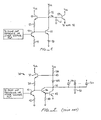
- FIG. 2 is a schematic diagram of a typical column clamp network 30 known in the prior art.
- a transistor 37 has its base connected through resistor 38 to V , and the collector is also connected to V .
- cc cc The emitter of transistor 37 is coupled through a resistor 39 to the collector of transistor 41.
- the base of transistor 41 is connected to a fixed bandgap reference voltage (e.g., 1.3v), and the emitter is connected through resistor 42 to ground.
- the bandgap reference voltage is translated through the base-emitter drop of transistor 41, establishing a current through resistor 42 to ground. This current is mirrored by the collector of transistor 41 to create a voltage across resistor 39.
- the voltage drop across resistor 39 is applied across the base-emitter junction of transistor 37, establishing a reference voltage at node 43.
- Node 43 is connected through diode 44 to the array reference node 32.
- Transistors 46 and 47 are connected between the collector of transistor 41 and node 32 and ground in a high level driver configuration to provide a current sinking path directly to ground.
- the voltage drop across diode 44 sets the clamp voltage level at node 32 at 2V be plus the voltage drop across resistor 39.
- a negative feedback loop comprising transistor 37, diode 44, and resistor 39 maintains the voltage level by reducing base drive to transistor 37 when the output falls below the predetermined value, and increasing the base drive at elevated voltages.
- the reference node 32 is also connected to all of the diodes 31a-31n. Each of these diodes has an intrinsic capacitance, and their sum comprises a substantial capacitance, represented schematically by capacitor 50 connected to the node 32.
- a large current drop may occur at node 32 if an appropriate AC data pattern is fused into the array such that many or all of the product terms are sunk by a single word driver at the same time.
- the high level clamp driver composed of transistors 46 and 47 will momentarily continue to draw a large collector load, although the word driver is now sinking this current. As a result, a negative voltage spike will occur at node 32.
- the duration of the negative voltage spike is determined by the RC rise time of the node 32, which in turn is established by the resistor 38 and the large parasitic capacitance 50.
- the resulting RC rise time is depicted in Figure 3b. A substantial portion of that rise time represents a period in which the sense amplifiers cannot acquire a single or low number of rising bit line signals, and thus limits the operating speed of the logic array.
- the deglitching network of the present invention reduces the magnitude and duration of the negative voltage spike to' tolerable levels.
- the deglitching network is connected in parallel with the column clamp, and is designed to provide a transient current spike into reference node 32 when the voltage level of node 32 drops below a predetermined noise margin.
- a transistor 51 has its base connected through resistor 52 to V , and its collector also connected to V .
- the emitter of cc transistor 51 is coupled through a resistor 53 to the collector of transistor 54.
- the base of transistor 54 is connected to a fixed bandgap reference voltage (e.g., 1.3v), or similar voltage reference and the emitter is connected through resistor 55 to ground.
- the bandgap reference voltage is translated through the base-emitter drop of transistor 54, establishing a current through resistor 55 to ground. This current is mirrored by the collector of transistor 54, establishing a voltage across resistor 53.
- the voltage drop across resistor 53 is applied across the base-emitter junction of transistor 51, establishing a reference voltage at node 56 equal to 3V be plus the voltage drop across resistor 53.
- a feedback loop similar to the feedback loop described in the column clamp network varies the base drive to transistor 51 to maintain a constant voltage at node 56.
- the deglitching network also includes a transistor 59 having a collector connected directly to V , and the emitter connected directly to reference node 32.
- the base of transistor 59 is connected through capacitor 61 to ground, and also to node 56.
- Transistor 59 when actuated, forms a low impedance path directly from V to the reference node 32, so that a large amount of current may be delivered to the reference node 32 when that node voltage falls suddenly, as described above.
- Capacitor 61 is provided for added base drive should the transistor 59 be required to deliver an extraordinary amount of current without consuming DC power.
- the circuit configuration of the deglitching network is intentionally similar to that of the column clamp so both networks will track closely over the operating temperature range.
- the deglitching circuit includes a transistor 57 having the collector connected to node 56 and the emitter coupled through diode 58 to ground. The base of transistor 57 is connected directly to the collector of transistor 55.
- the component values are chosen so that the node 56 of the deglitching network is maintained, for example, 120mv lower than the voltage at node 43 of the column clamp network.
- transistor 59 requires greater than 120mv forward bias to switch on and conduct.
- any negative excursion of node 32 with respect to node 56 exceeding -120mv will forward bias and actuate transistor 59 and initiate a low level clamping action approximately equal to the high level clamp voltage.
- transistor 59 is reverse biased to turn off, and no further low level clamping action will occur.
- the overall result, depicted in Figure 3c is that the magnitude and rise time of the negative excursion is substantially reduced or even eliminated, and the access time of the logic array is likewise reduced.
- the deglitching network of the present invention has been described in use specifically to stabilize the bit sense nodes of a logic array in conjunction with a column voltage clamp network.
- the deglitching network may be viewed as a low level clamping network connected in parallel with a high level clamping network and adapted to correct the inherent tracking error of the high level clamping network under severe load shifting conditions.
- the high level voltage clamping network may be required to sink 40 milliamps at maximum load conditions, yet the load may drop to 400 microamps within an extremely brief period, in the nanosecond range. It is only in this circumstance that the deglitching network is actuated to inject current into the voltage reference node, and only until the high level driver transistors restabilize the voltage.
- the deglitching network may be applied to any voltage clamped node situation in which large load variations cause large voltage fluctuations of the clamped node.
Landscapes
- Physics & Mathematics (AREA)
- Engineering & Computer Science (AREA)
- Computer Hardware Design (AREA)
- Computing Systems (AREA)
- General Engineering & Computer Science (AREA)
- Mathematical Physics (AREA)
- Nonlinear Science (AREA)
- Logic Circuits (AREA)
- Electronic Switches (AREA)
- Manipulation Of Pulses (AREA)
Applications Claiming Priority (2)
| Application Number | Priority Date | Filing Date | Title |
|---|---|---|---|
| US731811 | 1985-05-07 | ||
| US06/731,811 US4763027A (en) | 1985-05-07 | 1985-05-07 | Deglitching network for digital logic circuits |
Publications (3)
| Publication Number | Publication Date |
|---|---|
| EP0201429A2 true EP0201429A2 (fr) | 1986-11-12 |
| EP0201429A3 EP0201429A3 (en) | 1988-09-21 |
| EP0201429B1 EP0201429B1 (fr) | 1992-11-11 |
Family
ID=24941046
Family Applications (1)
| Application Number | Title | Priority Date | Filing Date |
|---|---|---|---|
| EP86400982A Expired EP0201429B1 (fr) | 1985-05-07 | 1986-05-07 | Dispositif antiparasite pour circuits logiques numériques |
Country Status (5)
| Country | Link |
|---|---|
| US (1) | US4763027A (fr) |
| EP (1) | EP0201429B1 (fr) |
| JP (1) | JPS6258723A (fr) |
| CA (1) | CA1279109C (fr) |
| DE (1) | DE3687081T2 (fr) |
Cited By (2)
| Publication number | Priority date | Publication date | Assignee | Title |
|---|---|---|---|---|
| WO1988007791A1 (fr) * | 1987-03-23 | 1988-10-06 | Unisys Corporation | Circuit de terminaison d'une ligne de transmission de faible bruit |
| EP0375998A3 (fr) * | 1988-12-29 | 1991-03-13 | Motorola, Inc. | Circuit de suppression d'effets transitoires à faible puissance |
Family Cites Families (13)
| Publication number | Priority date | Publication date | Assignee | Title |
|---|---|---|---|---|
| DE1182288B (de) * | 1963-11-16 | 1964-11-26 | Boelkow Entwicklungen Kg | Schaltungsanordnung zur Einstellung der Ampitude einer von einem Pulsgenerator erzeugten Pulsspannung |
| US3350573A (en) * | 1964-09-14 | 1967-10-31 | Potter Instrument Co Inc | Circuit for suppressing noise when switching between various a-c sources superimposed on different d-c biases |
| US3521141A (en) * | 1967-10-30 | 1970-07-21 | Ibm | Leakage controlled electric charge switching and storing circuitry |
| US3937988A (en) * | 1974-04-05 | 1976-02-10 | Fairchild Camera And Instrument Corporation | Active termination network for clamping a line signal |
| US4027177A (en) * | 1975-03-05 | 1977-05-31 | Motorola, Inc. | Clamping circuit |
| JPS6053924B2 (ja) * | 1978-04-05 | 1985-11-28 | 株式会社東芝 | リミツタ回路 |
| US4242605A (en) * | 1978-05-22 | 1980-12-30 | Motorola, Inc. | Transient array drive for bipolar ROM/PROM |
| US4237414A (en) * | 1978-12-08 | 1980-12-02 | Motorola, Inc. | High impedance output current source |
| JPS55105438A (en) * | 1979-02-07 | 1980-08-13 | Nec Corp | Logic array |
| JPS5825712A (ja) * | 1981-08-07 | 1983-02-16 | Hitachi Ltd | 増幅回路 |
| US4587442A (en) * | 1983-12-01 | 1986-05-06 | Motorola, Inc. | Current threshold detector |
| DE3404317A1 (de) * | 1984-02-08 | 1985-08-08 | Robert Bosch Gmbh, 7000 Stuttgart | Schutzschaltung fuer durch elektrische signale gesteuerte geraete |
| US4620115A (en) * | 1984-09-07 | 1986-10-28 | Advanced Micro Devices, Inc. | Voltage-temperature compensated threshold for hysteresis line receiver at TTL supply voltage |
-
1985
- 1985-05-07 US US06/731,811 patent/US4763027A/en not_active Expired - Lifetime
-
1986
- 1986-05-06 CA CA000508470A patent/CA1279109C/fr not_active Expired - Lifetime
- 1986-05-07 JP JP61103249A patent/JPS6258723A/ja active Pending
- 1986-05-07 DE DE8686400982T patent/DE3687081T2/de not_active Expired - Lifetime
- 1986-05-07 EP EP86400982A patent/EP0201429B1/fr not_active Expired
Cited By (2)
| Publication number | Priority date | Publication date | Assignee | Title |
|---|---|---|---|---|
| WO1988007791A1 (fr) * | 1987-03-23 | 1988-10-06 | Unisys Corporation | Circuit de terminaison d'une ligne de transmission de faible bruit |
| EP0375998A3 (fr) * | 1988-12-29 | 1991-03-13 | Motorola, Inc. | Circuit de suppression d'effets transitoires à faible puissance |
Also Published As
| Publication number | Publication date |
|---|---|
| US4763027A (en) | 1988-08-09 |
| EP0201429B1 (fr) | 1992-11-11 |
| EP0201429A3 (en) | 1988-09-21 |
| DE3687081T2 (de) | 1993-05-13 |
| DE3687081D1 (de) | 1992-12-17 |
| CA1279109C (fr) | 1991-01-15 |
| JPS6258723A (ja) | 1987-03-14 |
Similar Documents
| Publication | Publication Date | Title |
|---|---|---|
| KR950005023B1 (ko) | Ecl게이트의 전력소비를 변화시키는 장치 및 ecl회로를 동작시키는 방법 | |
| US3619659A (en) | Integrator amplifier circuit with voltage regulation and temperature compensation | |
| JPH0328850B2 (fr) | ||
| EP0173288A2 (fr) | Circuit convertisseur de niveau de tension | |
| US4599521A (en) | Bias circuit with voltage and temperature compensation for an emitter coupled logic circuit | |
| US4400635A (en) | Wide temperature range switching circuit | |
| US4366397A (en) | Level conversion circuit | |
| US4039867A (en) | Current switch circuit having an active load | |
| US4763027A (en) | Deglitching network for digital logic circuits | |
| US5041747A (en) | Delay regulation circuit | |
| EP0207962B1 (fr) | Circuit de commande a trois etats | |
| US4485352A (en) | Current amplifier | |
| KR950015208B1 (ko) | 쇼트키 전류 모우드 논리 회로 | |
| US4675554A (en) | NPN transient driver circuit | |
| US4567381A (en) | Bias network having one mode for producing a regulated output | |
| US4980578A (en) | Fast sense amplifier | |
| US5097153A (en) | TTL compatible BICMOS input circuit | |
| US5126593A (en) | Method and circuitry for reducing output transients resulting from internal ground instabilities | |
| US4166964A (en) | Inverting buffer circuit | |
| IE53407B1 (en) | Transistor circuit | |
| US4978871A (en) | Level shift circuit for converting a signal referenced to a positive voltage to a signal referenced to a lower voltage | |
| JP2987971B2 (ja) | レベル変換回路 | |
| JP2001320122A (ja) | 駆動回路および半導体レーザ駆動装置 | |
| JP2577425B2 (ja) | 駆動回路 | |
| EP0203700A2 (fr) | Convertisseur de niveau logique |
Legal Events
| Date | Code | Title | Description |
|---|---|---|---|
| PUAI | Public reference made under article 153(3) epc to a published international application that has entered the european phase |
Free format text: ORIGINAL CODE: 0009012 |
|
| AK | Designated contracting states |
Kind code of ref document: A2 Designated state(s): DE FR GB IT NL |
|
| PUAL | Search report despatched |
Free format text: ORIGINAL CODE: 0009013 |
|
| AK | Designated contracting states |
Kind code of ref document: A3 Designated state(s): DE FR GB IT NL |
|
| 17P | Request for examination filed |
Effective date: 19890222 |
|
| 17Q | First examination report despatched |
Effective date: 19890913 |
|
| GRAA | (expected) grant |
Free format text: ORIGINAL CODE: 0009210 |
|
| AK | Designated contracting states |
Kind code of ref document: B1 Designated state(s): DE FR GB IT NL |
|
| REF | Corresponds to: |
Ref document number: 3687081 Country of ref document: DE Date of ref document: 19921217 |
|
| ET | Fr: translation filed | ||
| ITF | It: translation for a ep patent filed | ||
| PLBE | No opposition filed within time limit |
Free format text: ORIGINAL CODE: 0009261 |
|
| STAA | Information on the status of an ep patent application or granted ep patent |
Free format text: STATUS: NO OPPOSITION FILED WITHIN TIME LIMIT |
|
| 26N | No opposition filed | ||
| PGFP | Annual fee paid to national office [announced via postgrant information from national office to epo] |
Ref country code: GB Payment date: 19940412 Year of fee payment: 9 |
|
| PGFP | Annual fee paid to national office [announced via postgrant information from national office to epo] |
Ref country code: FR Payment date: 19940513 Year of fee payment: 9 |
|
| PGFP | Annual fee paid to national office [announced via postgrant information from national office to epo] |
Ref country code: NL Payment date: 19940531 Year of fee payment: 9 |
|
| PG25 | Lapsed in a contracting state [announced via postgrant information from national office to epo] |
Ref country code: GB Effective date: 19950507 |
|
| PG25 | Lapsed in a contracting state [announced via postgrant information from national office to epo] |
Ref country code: NL Effective date: 19951201 |
|
| GBPC | Gb: european patent ceased through non-payment of renewal fee |
Effective date: 19950507 |
|
| NLV4 | Nl: lapsed or anulled due to non-payment of the annual fee |
Effective date: 19951201 |
|
| PG25 | Lapsed in a contracting state [announced via postgrant information from national office to epo] |
Ref country code: FR Effective date: 19960229 |
|
| REG | Reference to a national code |
Ref country code: FR Ref legal event code: ST |
|
| REG | Reference to a national code |
Ref country code: FR Ref legal event code: ST |
|
| PG25 | Lapsed in a contracting state [announced via postgrant information from national office to epo] |
Ref country code: IT Free format text: LAPSE BECAUSE OF NON-PAYMENT OF DUE FEES;WARNING: LAPSES OF ITALIAN PATENTS WITH EFFECTIVE DATE BEFORE 2007 MAY HAVE OCCURRED AT ANY TIME BEFORE 2007. THE CORRECT EFFECTIVE DATE MAY BE DIFFERENT FROM THE ONE RECORDED. Effective date: 20050507 |
|
| PGFP | Annual fee paid to national office [announced via postgrant information from national office to epo] |
Ref country code: DE Payment date: 20050630 Year of fee payment: 20 |