EP0201453A2 - Cellules solaires à base de CuInS2 et leur procédé de fabrication - Google Patents
Cellules solaires à base de CuInS2 et leur procédé de fabrication Download PDFInfo
- Publication number
- EP0201453A2 EP0201453A2 EP86730080A EP86730080A EP0201453A2 EP 0201453 A2 EP0201453 A2 EP 0201453A2 EP 86730080 A EP86730080 A EP 86730080A EP 86730080 A EP86730080 A EP 86730080A EP 0201453 A2 EP0201453 A2 EP 0201453A2
- Authority
- EP
- European Patent Office
- Prior art keywords
- solar cell
- semiconductor material
- cell according
- marked
- mixing ratio
- Prior art date
- Legal status (The legal status is an assumption and is not a legal conclusion. Google has not performed a legal analysis and makes no representation as to the accuracy of the status listed.)
- Granted
Links
- 238000000034 method Methods 0.000 title claims abstract description 16
- 239000004065 semiconductor Substances 0.000 claims abstract description 53
- 239000000463 material Substances 0.000 claims abstract description 49
- 239000000203 mixture Substances 0.000 claims abstract description 7
- 230000008569 process Effects 0.000 claims abstract description 7
- 239000010949 copper Substances 0.000 claims description 22
- 239000007789 gas Substances 0.000 claims description 18
- 229910052751 metal Inorganic materials 0.000 claims description 13
- 239000002184 metal Substances 0.000 claims description 13
- 238000002156 mixing Methods 0.000 claims description 13
- 230000015572 biosynthetic process Effects 0.000 claims description 11
- 238000004519 manufacturing process Methods 0.000 claims description 11
- 238000012986 modification Methods 0.000 claims description 8
- 229910052709 silver Inorganic materials 0.000 claims description 8
- 239000004332 silver Substances 0.000 claims description 8
- 238000003786 synthesis reaction Methods 0.000 claims description 8
- 239000008151 electrolyte solution Substances 0.000 claims description 7
- 229910001369 Brass Inorganic materials 0.000 claims description 6
- NINIDFKCEFEMDL-UHFFFAOYSA-N Sulfur Chemical compound [S] NINIDFKCEFEMDL-UHFFFAOYSA-N 0.000 claims description 6
- 239000010951 brass Substances 0.000 claims description 6
- 229910052802 copper Inorganic materials 0.000 claims description 6
- 230000009467 reduction Effects 0.000 claims description 6
- 229920002379 silicone rubber Polymers 0.000 claims description 6
- 239000004945 silicone rubber Substances 0.000 claims description 6
- RYGMFSIKBFXOCR-UHFFFAOYSA-N Copper Chemical compound [Cu] RYGMFSIKBFXOCR-UHFFFAOYSA-N 0.000 claims description 5
- 229910000807 Ga alloy Inorganic materials 0.000 claims description 5
- 229910045601 alloy Inorganic materials 0.000 claims description 5
- 239000000956 alloy Substances 0.000 claims description 5
- 239000013078 crystal Substances 0.000 claims description 5
- 238000010292 electrical insulation Methods 0.000 claims description 5
- 230000004048 modification Effects 0.000 claims description 5
- 229910052717 sulfur Inorganic materials 0.000 claims description 5
- 239000011593 sulfur Substances 0.000 claims description 5
- 229910000846 In alloy Inorganic materials 0.000 claims description 4
- ZOMNIUBKTOKEHS-UHFFFAOYSA-L dimercury dichloride Chemical compound Cl[Hg][Hg]Cl ZOMNIUBKTOKEHS-UHFFFAOYSA-L 0.000 claims description 4
- 239000003792 electrolyte Substances 0.000 claims description 4
- 229910052738 indium Inorganic materials 0.000 claims description 4
- 238000004381 surface treatment Methods 0.000 claims description 4
- IJGRMHOSHXDMSA-UHFFFAOYSA-N Atomic nitrogen Chemical compound N#N IJGRMHOSHXDMSA-UHFFFAOYSA-N 0.000 claims description 3
- 239000007864 aqueous solution Substances 0.000 claims description 3
- 238000007664 blowing Methods 0.000 claims description 3
- 239000006227 byproduct Substances 0.000 claims description 3
- 229940075397 calomel Drugs 0.000 claims description 3
- 229910001873 dinitrogen Inorganic materials 0.000 claims description 3
- 238000001704 evaporation Methods 0.000 claims description 3
- 239000007788 liquid Substances 0.000 claims description 3
- 239000000126 substance Substances 0.000 claims description 3
- 238000012549 training Methods 0.000 claims description 3
- 238000001816 cooling Methods 0.000 claims description 2
- 238000005530 etching Methods 0.000 claims description 2
- 238000000265 homogenisation Methods 0.000 claims description 2
- 239000000155 melt Substances 0.000 claims description 2
- 238000005498 polishing Methods 0.000 claims description 2
- 238000011946 reduction process Methods 0.000 claims description 2
- 239000007858 starting material Substances 0.000 claims description 2
- 238000006243 chemical reaction Methods 0.000 abstract description 8
- 239000010931 gold Substances 0.000 description 9
- 229910052737 gold Inorganic materials 0.000 description 7
- PCHJSUWPFVWCPO-UHFFFAOYSA-N gold Chemical compound [Au] PCHJSUWPFVWCPO-UHFFFAOYSA-N 0.000 description 6
- BQCADISMDOOEFD-UHFFFAOYSA-N Silver Chemical compound [Ag] BQCADISMDOOEFD-UHFFFAOYSA-N 0.000 description 5
- 239000000243 solution Substances 0.000 description 5
- PZNSFCLAULLKQX-UHFFFAOYSA-N Boron nitride Chemical compound N#B PZNSFCLAULLKQX-UHFFFAOYSA-N 0.000 description 4
- PXHVJJICTQNCMI-UHFFFAOYSA-N Nickel Chemical compound [Ni] PXHVJJICTQNCMI-UHFFFAOYSA-N 0.000 description 4
- 239000011651 chromium Substances 0.000 description 4
- 238000005259 measurement Methods 0.000 description 4
- 238000010521 absorption reaction Methods 0.000 description 3
- 230000005540 biological transmission Effects 0.000 description 3
- 230000000694 effects Effects 0.000 description 3
- 230000005611 electricity Effects 0.000 description 3
- 239000011521 glass Substances 0.000 description 3
- OKTJSMMVPCPJKN-UHFFFAOYSA-N Carbon Chemical compound [C] OKTJSMMVPCPJKN-UHFFFAOYSA-N 0.000 description 2
- VYZAMTAEIAYCRO-UHFFFAOYSA-N Chromium Chemical compound [Cr] VYZAMTAEIAYCRO-UHFFFAOYSA-N 0.000 description 2
- 230000008901 benefit Effects 0.000 description 2
- 229910052799 carbon Inorganic materials 0.000 description 2
- 239000004020 conductor Substances 0.000 description 2
- 238000005260 corrosion Methods 0.000 description 2
- 230000007797 corrosion Effects 0.000 description 2
- 238000013461 design Methods 0.000 description 2
- 238000010586 diagram Methods 0.000 description 2
- 239000003822 epoxy resin Substances 0.000 description 2
- APFVFJFRJDLVQX-UHFFFAOYSA-N indium atom Chemical compound [In] APFVFJFRJDLVQX-UHFFFAOYSA-N 0.000 description 2
- 229910052759 nickel Inorganic materials 0.000 description 2
- 229920000647 polyepoxide Polymers 0.000 description 2
- VYPSYNLAJGMNEJ-UHFFFAOYSA-N silicon dioxide Inorganic materials O=[Si]=O VYPSYNLAJGMNEJ-UHFFFAOYSA-N 0.000 description 2
- 238000002490 spark plasma sintering Methods 0.000 description 2
- 230000003595 spectral effect Effects 0.000 description 2
- 229920003002 synthetic resin Polymers 0.000 description 2
- 239000000057 synthetic resin Substances 0.000 description 2
- 229910000497 Amalgam Inorganic materials 0.000 description 1
- 206010013786 Dry skin Diseases 0.000 description 1
- 241001295925 Gegenes Species 0.000 description 1
- 230000018199 S phase Effects 0.000 description 1
- 229920004482 WACKER® Polymers 0.000 description 1
- 229910052782 aluminium Inorganic materials 0.000 description 1
- XAGFODPZIPBFFR-UHFFFAOYSA-N aluminium Chemical compound [Al] XAGFODPZIPBFFR-UHFFFAOYSA-N 0.000 description 1
- 239000003708 ampul Substances 0.000 description 1
- 239000007795 chemical reaction product Substances 0.000 description 1
- 229910052804 chromium Inorganic materials 0.000 description 1
- 238000007796 conventional method Methods 0.000 description 1
- 239000002826 coolant Substances 0.000 description 1
- 238000011161 development Methods 0.000 description 1
- 238000005566 electron beam evaporation Methods 0.000 description 1
- 230000008020 evaporation Effects 0.000 description 1
- 239000012467 final product Substances 0.000 description 1
- 230000004907 flux Effects 0.000 description 1
- 150000002343 gold Chemical class 0.000 description 1
- 238000010438 heat treatment Methods 0.000 description 1
- 238000011065 in-situ storage Methods 0.000 description 1
- 238000002844 melting Methods 0.000 description 1
- 230000008018 melting Effects 0.000 description 1
- 229910044991 metal oxide Inorganic materials 0.000 description 1
- 150000004706 metal oxides Chemical class 0.000 description 1
- 238000001465 metallisation Methods 0.000 description 1
- 150000002739 metals Chemical class 0.000 description 1
- 230000003287 optical effect Effects 0.000 description 1
- 238000005036 potential barrier Methods 0.000 description 1
- 239000000047 product Substances 0.000 description 1
- 239000010453 quartz Substances 0.000 description 1
- 239000002994 raw material Substances 0.000 description 1
- 229910052710 silicon Inorganic materials 0.000 description 1
- 239000010703 silicon Substances 0.000 description 1
- 239000007787 solid Substances 0.000 description 1
- 238000001228 spectrum Methods 0.000 description 1
- 239000007921 spray Substances 0.000 description 1
- 238000004544 sputter deposition Methods 0.000 description 1
- 238000003860 storage Methods 0.000 description 1
- 239000000758 substrate Substances 0.000 description 1
- 238000012360 testing method Methods 0.000 description 1
- 239000002699 waste material Substances 0.000 description 1
Images
Classifications
-
- H—ELECTRICITY
- H01—ELECTRIC ELEMENTS
- H01M—PROCESSES OR MEANS, e.g. BATTERIES, FOR THE DIRECT CONVERSION OF CHEMICAL ENERGY INTO ELECTRICAL ENERGY
- H01M14/00—Electrochemical current or voltage generators not provided for in groups H01M6/00 - H01M12/00; Manufacture thereof
- H01M14/005—Photoelectrochemical storage cells
-
- H—ELECTRICITY
- H01—ELECTRIC ELEMENTS
- H01G—CAPACITORS; CAPACITORS, RECTIFIERS, DETECTORS, SWITCHING DEVICES, LIGHT-SENSITIVE OR TEMPERATURE-SENSITIVE DEVICES OF THE ELECTROLYTIC TYPE
- H01G9/00—Electrolytic capacitors, rectifiers, detectors, switching devices, light-sensitive or temperature-sensitive devices; Processes of their manufacture
- H01G9/20—Light-sensitive devices
-
- H—ELECTRICITY
- H10—SEMICONDUCTOR DEVICES; ELECTRIC SOLID-STATE DEVICES NOT OTHERWISE PROVIDED FOR
- H10F—INORGANIC SEMICONDUCTOR DEVICES SENSITIVE TO INFRARED RADIATION, LIGHT, ELECTROMAGNETIC RADIATION OF SHORTER WAVELENGTH OR CORPUSCULAR RADIATION
- H10F71/00—Manufacture or treatment of devices covered by this subclass
-
- H—ELECTRICITY
- H10—SEMICONDUCTOR DEVICES; ELECTRIC SOLID-STATE DEVICES NOT OTHERWISE PROVIDED FOR
- H10F—INORGANIC SEMICONDUCTOR DEVICES SENSITIVE TO INFRARED RADIATION, LIGHT, ELECTROMAGNETIC RADIATION OF SHORTER WAVELENGTH OR CORPUSCULAR RADIATION
- H10F77/00—Constructional details of devices covered by this subclass
- H10F77/10—Semiconductor bodies
- H10F77/12—Active materials
- H10F77/126—Active materials comprising only Group I-III-VI chalcopyrite materials, e.g. CuInSe2, CuGaSe2 or CuInGaSe2 [CIGS]
-
- Y—GENERAL TAGGING OF NEW TECHNOLOGICAL DEVELOPMENTS; GENERAL TAGGING OF CROSS-SECTIONAL TECHNOLOGIES SPANNING OVER SEVERAL SECTIONS OF THE IPC; TECHNICAL SUBJECTS COVERED BY FORMER USPC CROSS-REFERENCE ART COLLECTIONS [XRACs] AND DIGESTS
- Y02—TECHNOLOGIES OR APPLICATIONS FOR MITIGATION OR ADAPTATION AGAINST CLIMATE CHANGE
- Y02E—REDUCTION OF GREENHOUSE GAS [GHG] EMISSIONS, RELATED TO ENERGY GENERATION, TRANSMISSION OR DISTRIBUTION
- Y02E10/00—Energy generation through renewable energy sources
- Y02E10/50—Photovoltaic [PV] energy
- Y02E10/541—CuInSe2 material PV cells
Definitions
- the invention relates to solar cells with a photoanode based on CuInS 2 semiconductor material and to processes for their production.
- Silicon has been particularly widespread as an active semiconductor material. In recent times efforts have also been made to use other materials for solid-state solar cells as well.
- the invention aims to create solar cells with corresponding photo anodes. Furthermore, specific details are to be shown for both photoelectrochemical and solid-state solar cells, which lead to the desired high efficiency with such photoanodes. In addition, there is also a task to specify which measures are to be taken mainly in order to manufacture such solar cells or to be able to synthesize the semiconductor material to be used for the photoanodes.
- a method specially developed for this purpose is also used to produce solar cells according to the invention ren proposed.
- the semiconductor material for photo anodes synthesized in this way is suitable for use in both photoelectrochemical and solid-state solar cells.
- the measures of this production process consist in the fact that for the synthesis of the photoactive semiconductor material in a closed container, which has a final vacuum of 10 -5 Torr
- the synthesis of the photoactive semiconductor material is therefore of essential importance for the technical teaching according to the invention. Lessons learned so far suggest that it is particularly important that In 2 S 3 is formed, namely outside the end product with a total share of about 0.1% of the weight of indium. In any case, samples, the synthesis of which had this effect, had excellent spectral properties and the above-mentioned high efficiency in converting solar energy into electricity in a photoelectrochemical test device.
- the metalli must - specific front contact to be transparent. This can be achieved in the case of area-covering metal films by their small thickness, but also by a lattice-like design of the metallization, expediently in connection with an intermediate film made of transparent, electrically conductive material between the metal lattice and the semiconductor material.
- the undoubtedly disadvantageous absorption of the incident light at one Comprehensive metal film must be compared with the advantages associated with its much simpler manufacture compared to SIS structures with a metal grid above it.
- the metal layer formed as a full-coverage film can also be provided with an antireflection layer, in order to limit inevitable losses essentially to absorption and not to increase them by avoidable reflection.
- the present invention therefore provides a solid-state solar cell that is simple to manufacture and easy to use, the metallic front contact being decisive for the formation of a Schottky contact structure with a large potential barrier and efficient charge collection.
- the optical properties of the CuInS2 semiconductor material and its energy gap of around 1.5 eV already offer optimal prerequisites in terms of solar energy conversion.
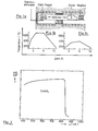
- the furnace is preferably equipped with two heating devices to be operated separately from one another. The temperatures set there can be monitored using thermocouples, one of which is shown. However, it is sufficient to provide only a heater and a sleeve on the laboratory scale, which thermally insulate the two ends of the piston from each other, and to blow or spray with a coolant the end of the piston at which the temperatures are lower than at the other end.
- Copper - Cu - and Indium - In - are placed as alloys in a crucible or boat made of pyrolytic boron nitride (PBN) at the end of the flask where the higher temperatures are to prevail.
- PBN pyrolytic boron nitride
- the sulfur - S - is deposited at the other end of the flask in a storage vessel with a fine nozzle.
- the temperature profiles at both ends of the flask are given in the two graphs as a function of time.
- the desired reactions take place, i.e. CuInS 2 crystals or crystallites with inclusions of In, Cu2-xS (0 - x ⁇ 1 ) and In 2 S 3 .
- In 2 S 3 also forms in the middle of the flask - In already at a temperature of 700 C of the Cu-In alloy or melt, In evaporates and reacts with part of the sulfur in the gas phase - and is deposited on the container wall . From the crowd outside the semiconductor ingot already incurred In 2 S 3 can be an indicator of M ATE rialzusammen arrangement in bullion pull this.
- the semiconductor bar has a length of approx. 100 mm and a diameter of approx. 10 mm.
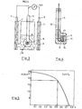
- the photoelectrochemical solar cell PECS shown in FIG. 3 has a chamber 1, in which the working electrode 4 is located, a secondary chamber 1 'with a reference electrode 7, which is used for scientific studies of the conversion process, but for the function of the solar cell PECS as a converter of light energy in electrical energy is not required, and a chamber 2 with the counter electrode 6.
- the counter electrode 6 and also the reference electrode 7 exist, for example from a carbon rod.
- the electrolyte solution 3, which at least partially wets the electrodes 4, 6, 7, is located in the chambers 1, 1 ', 2.
- a semiconductor plate 5 is attached, which is irradiated by a luminous flux 8.
- FIG. 4 shows the structure of a working electrode 4 with the contacting of the semiconductor die 5 in cross section.
- a layer 10 of In-Ga amalgam and an Ag synthetic resin layer 11 are applied between the rear side of the semiconductor chip 5 and the connecting wire 12.
- the connecting wire 12 is fastened to or in the synthetic resin layer 11 and, electrically insulated and sealed against corrosion, is guided to the outside.
- the fully contacted semiconductor chip 5 of the working electrode is also enclosed in an electrically insulating and corrosion-resistant manner by a suitable mass 13, e.g. Epoxy resin, glass or a silicone rubber, enclosed.
- the surface of the semiconductor die 5 must come into direct contact with the electrolyte liquid; when encasing, melting or the like. With the mass 13, care must therefore be taken that a window opening 14 remains open.
- This structure is essentially the same as that shown and described in EP-A-O 136 967, FIGS. 1 and 2.
- a special feature in the present case is the changed production of the back contact.
- An In-Ga alloy (mixing ratio 90: 10 mol%) forms the layer 10; the approx. 0.2 mm thick crystal plates are provided with a two-component conductive silver (3 M, A-B) and glued to a pre-polished brass holder.
- the brass sleeve is lined with silicone rubber (Wacker No. A 33).
- In 2 S 3 which is to be designated as a by-product or even as a waste product and forms outside the synthesized semiconductor material, allows simple conclusions to be drawn about the desired synthesis, so that this is also an advantage for the invention.
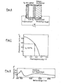
- the front contact for a solid-state solar cell according to FIG. 6 is produced in such a way that an electrode which has been assembled in accordance with the above-mentioned information is initially in an electrochemical solar cell, consisting of a working electrode (CuInS 2 ), counter electrode, electrode (carbon rod) and Reference electrode ( K alomel electrode), which are electrically connected to each other by a lead electrolyte consisting of 2.5 M CaJ 2 , 50 mM J 2 and 2 M HJ, for a period of 1 h in the potential range from 0 V to -0 , 4 V against calomel is cyclically polarized at a speed of 20 mV / s.
- the electrode surface is illuminated with an illuminance of approx. 250 mW / cm 2 illuminated.
- the solution is kept in air and not stirred.
- the distance between the electrode surface and the window of the cell is approx. 1 mm.
- the electrode is removed from the solution and the electrode surface is dried by blowing with nitrogen gas without any further treatment.
- the electrode is then immediately deposited, ie in a period of less than 60 s, in a vacuum system and the system is evacuated. At a pressure of less than 10 -3 Torr, a 200 & thick gold film is thermally evaporated onto the sample.
- a glass carrier was vaporized at the same distance from the same evaporation source for comparison purposes while working on the invention.
- the solid-state solar cell produced in this way is then to be conductively connected at one point on the electrode surface by silver epoxy resin (3M, A-B) to a Cu wire, as shown in FIG. 6.
- Measurements to determine the efficiency of solar energy conversion were carried out in such a way that the electrode surface to be illuminated was aligned with the sun until the photocurrent showed its maximum.
- the front contact was connected to the back contact via a resistor cascade and a current measuring device.
- the respective photocurrent value with the resistance set was measured and the voltage was determined in accordance with Ohm's law.
- the result for an electrode surface of 1.46 mm 2 on exposure is shown in FIG. 7.
- the illuminance was 64 mW / cm and was measured with a pyranometer from Kipp-Zonen.
- the absorption of the gold film by a multiplicative factor of 6.5 with regard to the illuminance is taken into account. This factor was determined by measuring the illuminance of the sun through the vapor-coated glass plate serving as the window (12.3 mW / cm 2 ) and comparing it with the value without using the window (81.1 mw / cm 2 ).
- the transmission of this gold film is shown in FIG. 8 and shows values between approximately 10% and 30% in the area of the sunlight spectrum.
Landscapes
- Engineering & Computer Science (AREA)
- Power Engineering (AREA)
- Chemical & Material Sciences (AREA)
- Chemical Kinetics & Catalysis (AREA)
- Electrochemistry (AREA)
- General Chemical & Material Sciences (AREA)
- Microelectronics & Electronic Packaging (AREA)
- Photovoltaic Devices (AREA)
Priority Applications (1)
| Application Number | Priority Date | Filing Date | Title |
|---|---|---|---|
| AT86730080T ATE93082T1 (de) | 1985-05-10 | 1986-05-09 | Solarzellen auf der basis von cuins2 und verfahren zu deren herstellung. |
Applications Claiming Priority (4)
| Application Number | Priority Date | Filing Date | Title |
|---|---|---|---|
| DE3517464 | 1985-05-10 | ||
| DE3517464 | 1985-05-10 | ||
| DE3536413 | 1985-10-10 | ||
| DE3536413 | 1985-10-10 |
Publications (3)
| Publication Number | Publication Date |
|---|---|
| EP0201453A2 true EP0201453A2 (fr) | 1986-11-12 |
| EP0201453A3 EP0201453A3 (en) | 1989-08-30 |
| EP0201453B1 EP0201453B1 (fr) | 1993-08-11 |
Family
ID=25832257
Family Applications (1)
| Application Number | Title | Priority Date | Filing Date |
|---|---|---|---|
| EP86730080A Expired - Lifetime EP0201453B1 (fr) | 1985-05-10 | 1986-05-09 | Cellules solaires à base de CuInS2 et leur procédé de fabrication |
Country Status (6)
| Country | Link |
|---|---|
| US (1) | US4687881A (fr) |
| EP (1) | EP0201453B1 (fr) |
| AT (1) | ATE93082T1 (fr) |
| CA (1) | CA1242785A (fr) |
| DE (2) | DE3688857D1 (fr) |
| IL (2) | IL78822A (fr) |
Cited By (1)
| Publication number | Priority date | Publication date | Assignee | Title |
|---|---|---|---|---|
| DE19504754A1 (de) * | 1995-02-03 | 1996-08-08 | Univ Leipzig | Photovoltaische und photoelektrische Bauteile |
Families Citing this family (13)
| Publication number | Priority date | Publication date | Assignee | Title |
|---|---|---|---|---|
| US5436204A (en) * | 1993-04-12 | 1995-07-25 | Midwest Research Institute | Recrystallization method to selenization of thin-film Cu(In,Ga)Se2 for semiconductor device applications |
| US5356839A (en) * | 1993-04-12 | 1994-10-18 | Midwest Research Institute | Enhanced quality thin film Cu(In,Ga)Se2 for semiconductor device applications by vapor-phase recrystallization |
| US5702185A (en) * | 1994-08-09 | 1997-12-30 | P. A. Hilton Limited | Heat flow transducer |
| US6107562A (en) * | 1998-03-24 | 2000-08-22 | Matsushita Electric Industrial Co., Ltd. | Semiconductor thin film, method for manufacturing the same, and solar cell using the same |
| US6259016B1 (en) | 1999-03-05 | 2001-07-10 | Matsushita Electric Industrial Co., Ltd. | Solar cell |
| DE19958878B4 (de) * | 1999-12-07 | 2012-01-19 | Saint-Gobain Glass Deutschland Gmbh | Dünnschicht-Solarzelle |
| JP4662616B2 (ja) | 2000-10-18 | 2011-03-30 | パナソニック株式会社 | 太陽電池 |
| DE10344315B3 (de) * | 2003-09-21 | 2004-12-09 | Hahn-Meitner-Institut Berlin Gmbh | Elektrochemisches Ätzverfahren zum selektiven Entfernen von Fremdphasen an der Oberfläche eines sulfidhaltigen Chalkopyrithalbeiters |
| US8324414B2 (en) | 2009-12-23 | 2012-12-04 | Battelle Energy Alliance, Llc | Methods of forming single source precursors, methods of forming polymeric single source precursors, and single source precursors and intermediate products formed by such methods |
| US9371226B2 (en) | 2011-02-02 | 2016-06-21 | Battelle Energy Alliance, Llc | Methods for forming particles |
| US8951446B2 (en) | 2008-03-13 | 2015-02-10 | Battelle Energy Alliance, Llc | Hybrid particles and associated methods |
| US8003070B2 (en) * | 2008-03-13 | 2011-08-23 | Battelle Energy Alliance, Llc | Methods for forming particles from single source precursors |
| US20140150850A1 (en) * | 2012-11-30 | 2014-06-05 | Amtech Systems, Inc. | Solar cell coating |
Family Cites Families (2)
| Publication number | Priority date | Publication date | Assignee | Title |
|---|---|---|---|---|
| US4601960A (en) * | 1983-08-24 | 1986-07-22 | Hahn-Meitner-Institut Fur Kernforschung Berlin Gmbh | Photoelectrochemical solar cell and method of fabricating a substrate for such a cell |
| US4559282A (en) * | 1984-09-20 | 1985-12-17 | The United States Of America As Represented By The United States Department Of Energy | Stable N-CuInSe2 /iodide-iodine photoelectrochemical cell |
-
1985
- 1985-05-18 IL IL78822A patent/IL78822A/xx not_active IP Right Cessation
-
1986
- 1986-05-09 AT AT86730080T patent/ATE93082T1/de active
- 1986-05-09 CA CA000508772A patent/CA1242785A/fr not_active Expired
- 1986-05-09 EP EP86730080A patent/EP0201453B1/fr not_active Expired - Lifetime
- 1986-05-09 DE DE8686730080T patent/DE3688857D1/de not_active Expired - Fee Related
- 1986-05-09 DE DE19863615889 patent/DE3615889A1/de not_active Withdrawn
- 1986-05-09 US US06/861,516 patent/US4687881A/en not_active Expired - Fee Related
- 1986-05-18 IL IL78822A patent/IL78822A0/xx unknown
Cited By (1)
| Publication number | Priority date | Publication date | Assignee | Title |
|---|---|---|---|---|
| DE19504754A1 (de) * | 1995-02-03 | 1996-08-08 | Univ Leipzig | Photovoltaische und photoelektrische Bauteile |
Also Published As
| Publication number | Publication date |
|---|---|
| ATE93082T1 (de) | 1993-08-15 |
| DE3688857D1 (de) | 1993-09-16 |
| US4687881A (en) | 1987-08-18 |
| EP0201453B1 (fr) | 1993-08-11 |
| IL78822A (en) | 1989-12-15 |
| IL78822A0 (en) | 1986-09-30 |
| DE3615889A1 (de) | 1986-11-13 |
| EP0201453A3 (en) | 1989-08-30 |
| CA1242785A (fr) | 1988-10-04 |
Similar Documents
| Publication | Publication Date | Title |
|---|---|---|
| EP0201453B1 (fr) | Cellules solaires à base de CuInS2 et leur procédé de fabrication | |
| EP0715358B2 (fr) | Méthode de fabrication d'une cellule solaire avec une couche d'absorption en chalcopyrite et cellule solaire ainsi produite | |
| EP0468094B1 (fr) | Procédé de fabrication d'une cellule solaire en chalcopyrite | |
| EP0721667B1 (fr) | Cellule solaire avec une couche d'absorption en chalcopyrite | |
| DE69325055T2 (de) | Orientierte polykristalline dünne Filme aus Übergangsmetallchalcogeniden | |
| DE10151415A1 (de) | Solarzelle | |
| DE4132882A1 (de) | Verfahren zur herstellung von pn cdte/cds-duennschichtsolarzellen | |
| EP0662247A1 (fr) | Procede rapide de realisation d'un semi-conducteur en chalcopyrite sur un substrat | |
| DE2639841B2 (de) | Solarzelle und Verfahren zu ihrer Herstellung | |
| DE2750607A1 (de) | Luftbestaendiges kristallines lithiumnitrid, verfahren zu seiner herstellung und seine verwendung | |
| DE102010003414A1 (de) | Verfahren zur Herstellung einer Solarzelle vom Chalcopyrit-Typ | |
| DE2806880C3 (de) | Solarzelle und Verfahren zu ihrer Herstellung | |
| EP1972014A1 (fr) | Matériau semi-conducteur actif photovoltaïque et cellule photovoltaïque | |
| DE3141241A1 (de) | Photoelektrische zelle | |
| DE10105986A1 (de) | Halbleiteranordnung mit kristallinem Silicium und Verfahren zu deren Herstellung | |
| DE69231288T2 (de) | Verfahren zur Herstellung einer Verbindungshalbleiter-Dünnschicht | |
| DE2251938C2 (de) | Legierung aus einer festen Lösung zur thermoelektrischen Energieumwandlung | |
| DE1564356A1 (de) | Verfahren zum Herstellen von photoelektrischen Zellen unter Verwendung von polykristallinen pulverfoermigen Stoffen | |
| DE3247869A1 (de) | Phosphorketten enthaltende substanzen | |
| WO1995009435A1 (fr) | Procede de production de couches microcristallines, et utilisation desdites couches | |
| DE3119631A1 (de) | "photovoltaische solarzelle" | |
| DE102005047907A1 (de) | Photovoltaische Zelle mit einem darin enthaltenen photovoltaisch aktiven Halbleitermaterial | |
| EP0136967B1 (fr) | Cellule solaire photoélectrochimique et procédé de fabrication d'une électrode de traveil pour cellules solaires | |
| EP0798786B1 (fr) | Cellule solaire comportant une couche d'absorption en chalcopyrite | |
| DE10004733C2 (de) | Dünnfilm-Halbleiterbauelement mit einer Chalkopyritschicht und Verfahren zu seiner Herstellung sowie Verwendung des Verfahrens zur Herstellung einer Dünnfilm-Solarzelle |
Legal Events
| Date | Code | Title | Description |
|---|---|---|---|
| PUAI | Public reference made under article 153(3) epc to a published international application that has entered the european phase |
Free format text: ORIGINAL CODE: 0009012 |
|
| AK | Designated contracting states |
Kind code of ref document: A2 Designated state(s): AT BE CH DE FR GB IT LI LU NL SE |
|
| RIN1 | Information on inventor provided before grant (corrected) |
Inventor name: HUSEMANN, KARL-DIETER, DIPL.-PHYS. Inventor name: FIECHTER, MANUEL, DR. RER. NAT. Inventor name: LEWERENZ, HANS-JOACHIM, DR. RER. NAT. Inventor name: GOSLOWSKY, HANS, DR. |
|
| RAP1 | Party data changed (applicant data changed or rights of an application transferred) |
Owner name: HAHN-MEITNER-INSTITUT BERLIN GESELLSCHAFT MIT BESC |
|
| PUAL | Search report despatched |
Free format text: ORIGINAL CODE: 0009013 |
|
| RHK1 | Main classification (correction) |
Ipc: H01G 9/20 |
|
| AK | Designated contracting states |
Kind code of ref document: A3 Designated state(s): AT BE CH DE FR GB IT LI LU NL SE |
|
| 17P | Request for examination filed |
Effective date: 19900105 |
|
| 17Q | First examination report despatched |
Effective date: 19910121 |
|
| GRAA | (expected) grant |
Free format text: ORIGINAL CODE: 0009210 |
|
| AK | Designated contracting states |
Kind code of ref document: B1 Designated state(s): AT BE CH DE FR GB IT LI LU NL SE |
|
| REF | Corresponds to: |
Ref document number: 93082 Country of ref document: AT Date of ref document: 19930815 Kind code of ref document: T |
|
| REF | Corresponds to: |
Ref document number: 3688857 Country of ref document: DE Date of ref document: 19930916 |
|
| GBT | Gb: translation of ep patent filed (gb section 77(6)(a)/1977) |
Effective date: 19930902 |
|
| ITF | It: translation for a ep patent filed | ||
| ET | Fr: translation filed | ||
| PGFP | Annual fee paid to national office [announced via postgrant information from national office to epo] |
Ref country code: GB Payment date: 19940412 Year of fee payment: 9 |
|
| PGFP | Annual fee paid to national office [announced via postgrant information from national office to epo] |
Ref country code: LU Payment date: 19940430 Year of fee payment: 9 |
|
| PGFP | Annual fee paid to national office [announced via postgrant information from national office to epo] |
Ref country code: BE Payment date: 19940503 Year of fee payment: 9 |
|
| PGFP | Annual fee paid to national office [announced via postgrant information from national office to epo] |
Ref country code: AT Payment date: 19940513 Year of fee payment: 9 |
|
| PGFP | Annual fee paid to national office [announced via postgrant information from national office to epo] |
Ref country code: CH Payment date: 19940517 Year of fee payment: 9 |
|
| PGFP | Annual fee paid to national office [announced via postgrant information from national office to epo] |
Ref country code: NL Payment date: 19940531 Year of fee payment: 9 |
|
| PLBE | No opposition filed within time limit |
Free format text: ORIGINAL CODE: 0009261 |
|
| STAA | Information on the status of an ep patent application or granted ep patent |
Free format text: STATUS: NO OPPOSITION FILED WITHIN TIME LIMIT |
|
| EPTA | Lu: last paid annual fee | ||
| 26N | No opposition filed | ||
| EAL | Se: european patent in force in sweden |
Ref document number: 86730080.8 |
|
| PGFP | Annual fee paid to national office [announced via postgrant information from national office to epo] |
Ref country code: SE Payment date: 19950508 Year of fee payment: 10 |
|
| PG25 | Lapsed in a contracting state [announced via postgrant information from national office to epo] |
Ref country code: LU Free format text: LAPSE BECAUSE OF NON-PAYMENT OF DUE FEES Effective date: 19950509 Ref country code: GB Effective date: 19950509 Ref country code: AT Effective date: 19950509 |
|
| PGFP | Annual fee paid to national office [announced via postgrant information from national office to epo] |
Ref country code: FR Payment date: 19950516 Year of fee payment: 10 |
|
| PG25 | Lapsed in a contracting state [announced via postgrant information from national office to epo] |
Ref country code: LI Effective date: 19950531 Ref country code: CH Effective date: 19950531 Ref country code: BE Effective date: 19950531 |
|
| PGFP | Annual fee paid to national office [announced via postgrant information from national office to epo] |
Ref country code: DE Payment date: 19950714 Year of fee payment: 10 |
|
| BERE | Be: lapsed |
Owner name: HAHN-MEITNER-INSTITUT BERLIN G.M.B.H. Effective date: 19950531 |
|
| PG25 | Lapsed in a contracting state [announced via postgrant information from national office to epo] |
Ref country code: NL Effective date: 19951201 |
|
| GBPC | Gb: european patent ceased through non-payment of renewal fee |
Effective date: 19950509 |
|
| REG | Reference to a national code |
Ref country code: CH Ref legal event code: PL |
|
| NLV4 | Nl: lapsed or anulled due to non-payment of the annual fee |
Effective date: 19951201 |
|
| PG25 | Lapsed in a contracting state [announced via postgrant information from national office to epo] |
Ref country code: SE Effective date: 19960510 |
|
| PG25 | Lapsed in a contracting state [announced via postgrant information from national office to epo] |
Ref country code: FR Effective date: 19970131 |
|
| PG25 | Lapsed in a contracting state [announced via postgrant information from national office to epo] |
Ref country code: DE Effective date: 19970201 |
|
| EUG | Se: european patent has lapsed |
Ref document number: 86730080.8 |
|
| REG | Reference to a national code |
Ref country code: FR Ref legal event code: ST |
|
| PG25 | Lapsed in a contracting state [announced via postgrant information from national office to epo] |
Ref country code: IT Free format text: LAPSE BECAUSE OF NON-PAYMENT OF DUE FEES;WARNING: LAPSES OF ITALIAN PATENTS WITH EFFECTIVE DATE BEFORE 2007 MAY HAVE OCCURRED AT ANY TIME BEFORE 2007. THE CORRECT EFFECTIVE DATE MAY BE DIFFERENT FROM THE ONE RECORDED. Effective date: 20050509 |