EP0201721A1 - Verfahren zur Herstellung eines halbleiterbauelementes mittels Ionenimplantation - Google Patents
Verfahren zur Herstellung eines halbleiterbauelementes mittels Ionenimplantation Download PDFInfo
- Publication number
- EP0201721A1 EP0201721A1 EP86104800A EP86104800A EP0201721A1 EP 0201721 A1 EP0201721 A1 EP 0201721A1 EP 86104800 A EP86104800 A EP 86104800A EP 86104800 A EP86104800 A EP 86104800A EP 0201721 A1 EP0201721 A1 EP 0201721A1
- Authority
- EP
- European Patent Office
- Prior art keywords
- species
- ions
- ion beam
- impurity ions
- implanted
- Prior art date
- Legal status (The legal status is an assumption and is not a legal conclusion. Google has not performed a legal analysis and makes no representation as to the accuracy of the status listed.)
- Granted
Links
Images



Classifications
-
- H—ELECTRICITY
- H10—SEMICONDUCTOR DEVICES; ELECTRIC SOLID-STATE DEVICES NOT OTHERWISE PROVIDED FOR
- H10P—GENERIC PROCESSES OR APPARATUS FOR THE MANUFACTURE OR TREATMENT OF DEVICES COVERED BY CLASS H10
- H10P30/00—Ion implantation into wafers, substrates or parts of devices
- H10P30/20—Ion implantation into wafers, substrates or parts of devices into semiconductor materials, e.g. for doping
-
- H—ELECTRICITY
- H10—SEMICONDUCTOR DEVICES; ELECTRIC SOLID-STATE DEVICES NOT OTHERWISE PROVIDED FOR
- H10D—INORGANIC ELECTRIC SEMICONDUCTOR DEVICES
- H10D84/00—Integrated devices formed in or on semiconductor substrates that comprise only semiconducting layers, e.g. on Si wafers or on GaAs-on-Si wafers
- H10D84/01—Manufacture or treatment
- H10D84/02—Manufacture or treatment characterised by using material-based technologies
- H10D84/05—Manufacture or treatment characterised by using material-based technologies using Group III-V technology
-
- H—ELECTRICITY
- H10—SEMICONDUCTOR DEVICES; ELECTRIC SOLID-STATE DEVICES NOT OTHERWISE PROVIDED FOR
- H10P—GENERIC PROCESSES OR APPARATUS FOR THE MANUFACTURE OR TREATMENT OF DEVICES COVERED BY CLASS H10
- H10P30/00—Ion implantation into wafers, substrates or parts of devices
- H10P30/20—Ion implantation into wafers, substrates or parts of devices into semiconductor materials, e.g. for doping
- H10P30/202—Ion implantation into wafers, substrates or parts of devices into semiconductor materials, e.g. for doping characterised by the semiconductor materials
- H10P30/206—Ion implantation into wafers, substrates or parts of devices into semiconductor materials, e.g. for doping characterised by the semiconductor materials into Group III-V semiconductors
-
- H—ELECTRICITY
- H10—SEMICONDUCTOR DEVICES; ELECTRIC SOLID-STATE DEVICES NOT OTHERWISE PROVIDED FOR
- H10P—GENERIC PROCESSES OR APPARATUS FOR THE MANUFACTURE OR TREATMENT OF DEVICES COVERED BY CLASS H10
- H10P30/00—Ion implantation into wafers, substrates or parts of devices
- H10P30/20—Ion implantation into wafers, substrates or parts of devices into semiconductor materials, e.g. for doping
- H10P30/21—Ion implantation into wafers, substrates or parts of devices into semiconductor materials, e.g. for doping of electrically active species
Definitions
- the present invention relates to a method of manufacturing a semiconductor device. More particularly, it relates to a method of manufacturing a semiconductor device which can introduce a plurality of species of impurities into a desired part without employing a mask.
- impurity ions have been implanted into a desired region by employing SiO 2 or resist for a mask and irradiating the region with an ion beam about 1 cm in diameter.
- an impurity doped region is rendered as small as possible.
- the registration accuracy between the masks becomes a problem. For example, the registration accuracy between the masks which is attained when electron beam lithography is employed is limited to approximately 0.15 pm for 3 ⁇ .
- an impurity can be introduced into a minute region within 0.1 pm.
- the positioning accuracy of the ion beams is inferior, so both the species of ions cannot be precisely implanted into the respective predetermined positions. This corresponds to the problem of the registration accuracy between the masks in the case of the conventional ion implantation and forms one serious problem in the practical application of the ion beams.
- An object of the present invention is to solve the problem of the prior art described above, and to provide a method of manufacturing a semiconductor device which can readily implant ions into a very small desired region at a high positional accuracy.
- the present invention for accomplishing the object is characterized by employing a focused ion beam which contains two or more species of impurity ions and which is so formed that the spacial distributions of ion current densities of the respective species are different.
- Figs. la and 1b are diagrams for explaining the principle of the present invention.
- a very fine focused ion beam 1 which consists of X + and Y ions (the ions may well be of three or more species) having different spacial distributions of ion current densities as shown in Fig. la is projected on a semiconductor substrate 2, whereby a plurality of implanted layers X and Y positioned to each other in self-alignment fashion are formed as shown in Fig. lb.
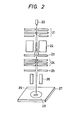
- numeral 20 designates a liquid metal ion source whose material to be ionized is an alloy containing a desired impurity
- numeral 21 a condenser lens assembly
- numeral 22 a mass separator which serves to separately derive only the ions of the desired impurity among impurity ions extracted from the liquid metal ion source 20
- numeral 23 a first aperture
- numeral 24 an objective lens assembly
- numeral 25 a second aperture
- numeral 26 an electrostatic deflector for deflecting a beam
- numeral 27 a workpiece holder
- numeral 28 a workpiece, for example, semiconductor substrate
- number 29 a focused ion beam.
- FIG. 3a shows the mass spectrum obtained when the electric field is varied
- Fig. 3b the mass spectrum obtained when the magnetic field is varied.
- the mass resolving power lowers, and a plurality of proximate spectra can be turned into a single spectrum.
- a mass spectrum shown in Fig. 4 can be realized by such processing. Referring to Fig.
- Fig. 6 is a view showing the section of a distributed feedback type semiconductor laser with an optical guide layer to which the present invention is applied.
- An undoped InGaAs active layer 67 being about 0.1 ⁇ m thick and an N-type InGaAs optical guide layer 64 being about 0.2 ⁇ m thick were epitaxially grown on an N-type InP substrate 68 being about 100 ⁇ m thick.
- a focused ion beam containing Si and Be ++ which had an acceleration energy of 50 - 100 keV and a beam diameter of 0.1 ⁇ m, is raster-scanned at pitches of 0.2 pm, whereby the ions were implanted within a dose range of 10 12 - 10 13 ions/cm to form Si ++ ion-implanted layers 65 and Be ++ ion-implanted layers 66.
- a P-type InP clad layer 63 being about 3 ⁇ m thick and a P-type InGaAsP cap layer 62 being about 0.3 ⁇ m thick were epitaxially grown, and a P-type electrode 61 and an N-type electrode 69 were formed.
- a laser device was fabricated.
- the optical guide layer 64 With the periodical P-N junction structure as described above, P-type carriers injected from the P-type electrode 61 are concentrated in the P-type regions 66 of low potential difference, so that the carrier density of the InGaAsP active layer 67 directly under the regions rises, and the effective refractive index thereof decreases. To the contrary, the carrier density lowers directly under the N-type regions 65, and the effective refractive index increases in this portion.
- the periodical P-N junction structure formed by the use of the present invention can establish a great effective index difference and can fabricate a single-wavelength laser.
- the periodical P-N junction structure of pitches of 0.2 ym which has not been realizable with the prior art can be formed by one time of ion implantation, and this is very effective as a method of manufacturing a semiconductor device having a minute structure.
- the present invention implants ions by the use of a focused ion beam containing a plurality of species of impurity ions, thereby making it possible to introduce a plurality of impurities into a minute region by one time of ion implantation without the positioning of ion beams.
- the invention can form, for example, a periodical P-N junction structure at pitches of 0.2 ⁇ m not having been realizable with the prior art, and the effect thereof is remarkable as a method of manufacturing future semiconductor devices having dimensions of the submicron order.
- This invention is not restricted only to the implantation of Si and Be into GaAs mentioned in the foregoing embodiment, but it is of course similarly applicable to a case of implanting different species of impurity ions into another semiconductor substrate in a similar way, such as a case of implanting boron (B + ) and arsenic (As) into silicon (Si).
Landscapes
- Semiconductor Lasers (AREA)
- Physical Vapour Deposition (AREA)
Applications Claiming Priority (2)
| Application Number | Priority Date | Filing Date | Title |
|---|---|---|---|
| JP60078347A JPS61237421A (ja) | 1985-04-15 | 1985-04-15 | 半導体装置の製造方法 |
| JP78347/85 | 1985-04-15 |
Publications (2)
| Publication Number | Publication Date |
|---|---|
| EP0201721A1 true EP0201721A1 (de) | 1986-11-20 |
| EP0201721B1 EP0201721B1 (de) | 1990-07-11 |
Family
ID=13659453
Family Applications (1)
| Application Number | Title | Priority Date | Filing Date |
|---|---|---|---|
| EP86104800A Expired - Lifetime EP0201721B1 (de) | 1985-04-15 | 1986-04-08 | Verfahren zur Herstellung eines halbleiterbauelementes mittels Ionenimplantation |
Country Status (4)
| Country | Link |
|---|---|
| US (1) | US4716127A (de) |
| EP (1) | EP0201721B1 (de) |
| JP (1) | JPS61237421A (de) |
| DE (1) | DE3672526D1 (de) |
Cited By (1)
| Publication number | Priority date | Publication date | Assignee | Title |
|---|---|---|---|---|
| EP0317952A3 (en) * | 1987-11-24 | 1990-01-31 | Hitachi, Ltd. | Device having superlattice structure, and method of and apparatus for manufacturing the same |
Families Citing this family (9)
| Publication number | Priority date | Publication date | Assignee | Title |
|---|---|---|---|---|
| US5026437A (en) * | 1990-01-22 | 1991-06-25 | Tencor Instruments | Cantilevered microtip manufacturing by ion implantation and etching |
| US6127211A (en) * | 1997-10-02 | 2000-10-03 | Matsushita Electric Industrial Co., Ltd. | Method of manufacturing transistor |
| US6995079B2 (en) * | 2003-08-29 | 2006-02-07 | Semiconductor Energy Laboratory Co., Ltd. | Ion implantation method and method for manufacturing semiconductor device |
| RU2285069C2 (ru) * | 2004-05-18 | 2006-10-10 | Объединенный Институт Ядерных Исследований | Способ многоэлементной ионной имплантации (варианты) |
| CN101248505B (zh) * | 2005-07-08 | 2010-12-15 | 耐克斯金思美控股公司 | 受控粒子束制造用的设备和方法 |
| WO2008140585A1 (en) | 2006-11-22 | 2008-11-20 | Nexgen Semi Holding, Inc. | Apparatus and method for conformal mask manufacturing |
| US10566169B1 (en) | 2008-06-30 | 2020-02-18 | Nexgen Semi Holding, Inc. | Method and device for spatial charged particle bunching |
| US10991545B2 (en) | 2008-06-30 | 2021-04-27 | Nexgen Semi Holding, Inc. | Method and device for spatial charged particle bunching |
| US12493005B1 (en) | 2022-06-07 | 2025-12-09 | Nexgen Semi Holding, Inc. | Extended range active illumination imager |
Citations (1)
| Publication number | Priority date | Publication date | Assignee | Title |
|---|---|---|---|---|
| EP0082640A2 (de) * | 1981-12-18 | 1983-06-29 | Kabushiki Kaisha Toshiba | Ionenimplantationsverfahren |
Family Cites Families (3)
| Publication number | Priority date | Publication date | Assignee | Title |
|---|---|---|---|---|
| US4385946A (en) * | 1981-06-19 | 1983-05-31 | Bell Telephone Laboratories, Incorporated | Rapid alteration of ion implant dopant species to create regions of opposite conductivity |
| JPS58164134A (ja) * | 1982-03-24 | 1983-09-29 | Hitachi Ltd | 半導体装置の製造方法 |
| US4556798A (en) * | 1983-07-12 | 1985-12-03 | Hughes Aircraft Company | Focused ion beam column |
-
1985
- 1985-04-15 JP JP60078347A patent/JPS61237421A/ja active Pending
-
1986
- 1986-04-08 DE DE8686104800T patent/DE3672526D1/de not_active Expired - Lifetime
- 1986-04-08 EP EP86104800A patent/EP0201721B1/de not_active Expired - Lifetime
- 1986-04-15 US US06/852,317 patent/US4716127A/en not_active Expired - Fee Related
Patent Citations (1)
| Publication number | Priority date | Publication date | Assignee | Title |
|---|---|---|---|---|
| EP0082640A2 (de) * | 1981-12-18 | 1983-06-29 | Kabushiki Kaisha Toshiba | Ionenimplantationsverfahren |
Non-Patent Citations (2)
| Title |
|---|
| IEEE ELECTRON DEVICE LETTERS, vol. EDL-2, no. 6, June 1981, pages 153-154, New York, US; R.L. KUBENA et al.: "GaAs MESFET fabrication using maskless ion implantation" * |
| JAPANESE JOURNAL OF APPLIED PHYSICS, vol. 22, no. 4, April 1983, pages L225-L226, Tokyo, JP; E. MIYAUCHI et al.: "Au-Si-Be Liquid metal ion source for maskless ion implantation" * |
Cited By (2)
| Publication number | Priority date | Publication date | Assignee | Title |
|---|---|---|---|---|
| EP0317952A3 (en) * | 1987-11-24 | 1990-01-31 | Hitachi, Ltd. | Device having superlattice structure, and method of and apparatus for manufacturing the same |
| US4983540A (en) * | 1987-11-24 | 1991-01-08 | Hitachi, Ltd. | Method of manufacturing devices having superlattice structures |
Also Published As
| Publication number | Publication date |
|---|---|
| JPS61237421A (ja) | 1986-10-22 |
| DE3672526D1 (de) | 1990-08-16 |
| EP0201721B1 (de) | 1990-07-11 |
| US4716127A (en) | 1987-12-29 |
Similar Documents
| Publication | Publication Date | Title |
|---|---|---|
| US3434894A (en) | Fabricating solid state devices by ion implantation | |
| US4074139A (en) | Apparatus and method for maskless ion implantation | |
| Melngailis | Focused ion beam technology and applications | |
| US5206516A (en) | Low energy, steered ion beam deposition system having high current at low pressure | |
| EP0339951A2 (de) | Optische Säule zur Erzeugung von stabförmigen Strahlen, dazugehörige Anordnung von bandförmigen Strahlen und geladene Partikel-Quelle | |
| EP0478215B1 (de) | Reflektionsmaske und eine solche Reflektionsmaske verwendendes geladenes Teilchenstrahl-Belichtungsgerät | |
| KR100843805B1 (ko) | 이온 비임을 생성하기 위한 이온 광학 장치 및 방법 | |
| DE3025945A1 (de) | Halbleiteranordnung und verfahren zu deren herstellung, sowie aufnahmeroehre und wiedergabevorrichtung mit einer derartigen halbleiteranordnung | |
| US4716127A (en) | Method of implanting spatially controlled P-N junctions by focused ion beams containing at least two species | |
| DE69315758T2 (de) | Implantationsgerät mittels fokusierten Ionenstrahls | |
| US5196706A (en) | Extractor and deceleration lens for ion beam deposition apparatus | |
| US4641034A (en) | Ion implantation apparatus and method for maskless processing | |
| KR20010089522A (ko) | 다중 대전된 입자 빔렛 방출 칼럼들의 어레이 | |
| WO1998048443A1 (en) | Multi-beam array electron optics | |
| NL8204240A (nl) | Halfgeleiderinrichting voor het emitteren van elektronen en inrichting voorzien van een dergelijke halfgeleiderinrichting. | |
| KR910002978B1 (ko) | 하전 입자 빔 리토그래픽 장치 및 방법 | |
| Brewer | The application of electron/ion beam technology to microelectronics | |
| JPH1187206A (ja) | 電子ビーム露光装置及び該装置を用いたデバイス製造方法 | |
| US4831628A (en) | Denices fabricated using method of selective area epitaxial growth using ion beams | |
| GB2337635A (en) | Method of forming a conducting structure on a substrate | |
| US4622093A (en) | Method of selective area epitaxial growth using ion beams | |
| US6028317A (en) | Charged particle beam optical element charged particle beam exposure apparatus and method of adjusting the same | |
| US4403400A (en) | Process for producing a semiconductor device | |
| US20230006043A1 (en) | System And Technique For Creating Implanted Regions Using Multiple Tilt Angles | |
| KR100560022B1 (ko) | 이온 주입 공정 |
Legal Events
| Date | Code | Title | Description |
|---|---|---|---|
| PUAI | Public reference made under article 153(3) epc to a published international application that has entered the european phase |
Free format text: ORIGINAL CODE: 0009012 |
|
| AK | Designated contracting states |
Kind code of ref document: A1 Designated state(s): DE FR GB |
|
| 17P | Request for examination filed |
Effective date: 19870326 |
|
| 17Q | First examination report despatched |
Effective date: 19890227 |
|
| GRAA | (expected) grant |
Free format text: ORIGINAL CODE: 0009210 |
|
| AK | Designated contracting states |
Kind code of ref document: B1 Designated state(s): DE FR GB |
|
| PG25 | Lapsed in a contracting state [announced via postgrant information from national office to epo] |
Ref country code: FR Effective date: 19900711 |
|
| REF | Corresponds to: |
Ref document number: 3672526 Country of ref document: DE Date of ref document: 19900816 |
|
| EN | Fr: translation not filed | ||
| PG25 | Lapsed in a contracting state [announced via postgrant information from national office to epo] |
Ref country code: GB Effective date: 19910408 |
|
| PLBE | No opposition filed within time limit |
Free format text: ORIGINAL CODE: 0009261 |
|
| STAA | Information on the status of an ep patent application or granted ep patent |
Free format text: STATUS: NO OPPOSITION FILED WITHIN TIME LIMIT |
|
| 26N | No opposition filed | ||
| GBPC | Gb: european patent ceased through non-payment of renewal fee | ||
| PGFP | Annual fee paid to national office [announced via postgrant information from national office to epo] |
Ref country code: DE Payment date: 19950626 Year of fee payment: 10 |
|
| PG25 | Lapsed in a contracting state [announced via postgrant information from national office to epo] |
Ref country code: DE Effective date: 19970101 |