EP0201860A2 - Mehrschichtige Anordnung mit einer die Kristallisation verhindernden Schicht und Verfahren zu ihrer Herstellung - Google Patents
Mehrschichtige Anordnung mit einer die Kristallisation verhindernden Schicht und Verfahren zu ihrer Herstellung Download PDFInfo
- Publication number
- EP0201860A2 EP0201860A2 EP86106237A EP86106237A EP0201860A2 EP 0201860 A2 EP0201860 A2 EP 0201860A2 EP 86106237 A EP86106237 A EP 86106237A EP 86106237 A EP86106237 A EP 86106237A EP 0201860 A2 EP0201860 A2 EP 0201860A2
- Authority
- EP
- European Patent Office
- Prior art keywords
- layer
- amorphous
- crystallization
- crystallizable
- layers
- Prior art date
- Legal status (The legal status is an assumption and is not a legal conclusion. Google has not performed a legal analysis and makes no representation as to the accuracy of the status listed.)
- Ceased
Links
Images
Classifications
-
- G—PHYSICS
- G03—PHOTOGRAPHY; CINEMATOGRAPHY; ANALOGOUS TECHNIQUES USING WAVES OTHER THAN OPTICAL WAVES; ELECTROGRAPHY; HOLOGRAPHY
- G03G—ELECTROGRAPHY; ELECTROPHOTOGRAPHY; MAGNETOGRAPHY
- G03G5/00—Recording-members for original recording by exposure, e.g. to light, to heat or to electrons; Manufacture thereof; Selection of materials therefor
- G03G5/02—Charge-receiving layers
- G03G5/04—Photoconductive layers; Charge-generation layers or charge-transporting layers; Additives therefor; Binders therefor
- G03G5/08—Photoconductive layers; Charge-generation layers or charge-transporting layers; Additives therefor; Binders therefor characterised by the photoconductive material being inorganic
- G03G5/082—Photoconductive layers; Charge-generation layers or charge-transporting layers; Additives therefor; Binders therefor characterised by the photoconductive material being inorganic and not being incorporated in a bonding material, e.g. vacuum deposited
-
- G—PHYSICS
- G11—INFORMATION STORAGE
- G11B—INFORMATION STORAGE BASED ON RELATIVE MOVEMENT BETWEEN RECORD CARRIER AND TRANSDUCER
- G11B7/00—Recording or reproducing by optical means, e.g. recording using a thermal beam of optical radiation by modifying optical properties or the physical structure, reproducing using an optical beam at lower power by sensing optical properties; Record carriers therefor
- G11B7/24—Record carriers characterised by shape, structure or physical properties, or by the selection of the material
- G11B7/241—Record carriers characterised by shape, structure or physical properties, or by the selection of the material characterised by the selection of the material
- G11B7/242—Record carriers characterised by shape, structure or physical properties, or by the selection of the material characterised by the selection of the material of recording layers
- G11B7/243—Record carriers characterised by shape, structure or physical properties, or by the selection of the material characterised by the selection of the material of recording layers comprising inorganic materials only, e.g. ablative layers
- G11B7/2433—Metals or elements of Groups 13, 14, 15 or 16 of the Periodic Table, e.g. B, Si, Ge, As, Sb, Bi, Se or Te
-
- G—PHYSICS
- G11—INFORMATION STORAGE
- G11B—INFORMATION STORAGE BASED ON RELATIVE MOVEMENT BETWEEN RECORD CARRIER AND TRANSDUCER
- G11B7/00—Recording or reproducing by optical means, e.g. recording using a thermal beam of optical radiation by modifying optical properties or the physical structure, reproducing using an optical beam at lower power by sensing optical properties; Record carriers therefor
- G11B7/24—Record carriers characterised by shape, structure or physical properties, or by the selection of the material
- G11B7/241—Record carriers characterised by shape, structure or physical properties, or by the selection of the material characterised by the selection of the material
- G11B7/252—Record carriers characterised by shape, structure or physical properties, or by the selection of the material characterised by the selection of the material of layers other than recording layers
- G11B7/257—Record carriers characterised by shape, structure or physical properties, or by the selection of the material characterised by the selection of the material of layers other than recording layers of layers having properties involved in recording or reproduction, e.g. optical interference layers or sensitising layers or dielectric layers, which are protecting the recording layers
- G11B7/2578—Record carriers characterised by shape, structure or physical properties, or by the selection of the material characterised by the selection of the material of layers other than recording layers of layers having properties involved in recording or reproduction, e.g. optical interference layers or sensitising layers or dielectric layers, which are protecting the recording layers consisting essentially of inorganic materials
-
- H—ELECTRICITY
- H10—SEMICONDUCTOR DEVICES; ELECTRIC SOLID-STATE DEVICES NOT OTHERWISE PROVIDED FOR
- H10N—ELECTRIC SOLID-STATE DEVICES NOT OTHERWISE PROVIDED FOR
- H10N70/00—Solid-state devices having no potential barriers, and specially adapted for rectifying, amplifying, oscillating or switching
-
- G—PHYSICS
- G11—INFORMATION STORAGE
- G11B—INFORMATION STORAGE BASED ON RELATIVE MOVEMENT BETWEEN RECORD CARRIER AND TRANSDUCER
- G11B7/00—Recording or reproducing by optical means, e.g. recording using a thermal beam of optical radiation by modifying optical properties or the physical structure, reproducing using an optical beam at lower power by sensing optical properties; Record carriers therefor
- G11B7/24—Record carriers characterised by shape, structure or physical properties, or by the selection of the material
- G11B7/241—Record carriers characterised by shape, structure or physical properties, or by the selection of the material characterised by the selection of the material
- G11B7/242—Record carriers characterised by shape, structure or physical properties, or by the selection of the material characterised by the selection of the material of recording layers
- G11B7/243—Record carriers characterised by shape, structure or physical properties, or by the selection of the material characterised by the selection of the material of recording layers comprising inorganic materials only, e.g. ablative layers
- G11B2007/24302—Metals or metalloids
- G11B2007/24312—Metals or metalloids group 14 elements (e.g. Si, Ge, Sn)
-
- G—PHYSICS
- G11—INFORMATION STORAGE
- G11B—INFORMATION STORAGE BASED ON RELATIVE MOVEMENT BETWEEN RECORD CARRIER AND TRANSDUCER
- G11B7/00—Recording or reproducing by optical means, e.g. recording using a thermal beam of optical radiation by modifying optical properties or the physical structure, reproducing using an optical beam at lower power by sensing optical properties; Record carriers therefor
- G11B7/24—Record carriers characterised by shape, structure or physical properties, or by the selection of the material
- G11B7/241—Record carriers characterised by shape, structure or physical properties, or by the selection of the material characterised by the selection of the material
- G11B7/242—Record carriers characterised by shape, structure or physical properties, or by the selection of the material characterised by the selection of the material of recording layers
- G11B7/243—Record carriers characterised by shape, structure or physical properties, or by the selection of the material characterised by the selection of the material of recording layers comprising inorganic materials only, e.g. ablative layers
- G11B2007/24302—Metals or metalloids
- G11B2007/24314—Metals or metalloids group 15 elements (e.g. Sb, Bi)
-
- G—PHYSICS
- G11—INFORMATION STORAGE
- G11B—INFORMATION STORAGE BASED ON RELATIVE MOVEMENT BETWEEN RECORD CARRIER AND TRANSDUCER
- G11B7/00—Recording or reproducing by optical means, e.g. recording using a thermal beam of optical radiation by modifying optical properties or the physical structure, reproducing using an optical beam at lower power by sensing optical properties; Record carriers therefor
- G11B7/24—Record carriers characterised by shape, structure or physical properties, or by the selection of the material
- G11B7/241—Record carriers characterised by shape, structure or physical properties, or by the selection of the material characterised by the selection of the material
- G11B7/242—Record carriers characterised by shape, structure or physical properties, or by the selection of the material characterised by the selection of the material of recording layers
- G11B7/243—Record carriers characterised by shape, structure or physical properties, or by the selection of the material characterised by the selection of the material of recording layers comprising inorganic materials only, e.g. ablative layers
- G11B2007/24302—Metals or metalloids
- G11B2007/24316—Metals or metalloids group 16 elements (i.e. chalcogenides, Se, Te)
-
- G—PHYSICS
- G11—INFORMATION STORAGE
- G11B—INFORMATION STORAGE BASED ON RELATIVE MOVEMENT BETWEEN RECORD CARRIER AND TRANSDUCER
- G11B7/00—Recording or reproducing by optical means, e.g. recording using a thermal beam of optical radiation by modifying optical properties or the physical structure, reproducing using an optical beam at lower power by sensing optical properties; Record carriers therefor
- G11B7/24—Record carriers characterised by shape, structure or physical properties, or by the selection of the material
- G11B7/241—Record carriers characterised by shape, structure or physical properties, or by the selection of the material characterised by the selection of the material
- G11B7/252—Record carriers characterised by shape, structure or physical properties, or by the selection of the material characterised by the selection of the material of layers other than recording layers
- G11B7/257—Record carriers characterised by shape, structure or physical properties, or by the selection of the material characterised by the selection of the material of layers other than recording layers of layers having properties involved in recording or reproduction, e.g. optical interference layers or sensitising layers or dielectric layers, which are protecting the recording layers
- G11B2007/25705—Record carriers characterised by shape, structure or physical properties, or by the selection of the material characterised by the selection of the material of layers other than recording layers of layers having properties involved in recording or reproduction, e.g. optical interference layers or sensitising layers or dielectric layers, which are protecting the recording layers consisting essentially of inorganic materials
- G11B2007/25708—Record carriers characterised by shape, structure or physical properties, or by the selection of the material characterised by the selection of the material of layers other than recording layers of layers having properties involved in recording or reproduction, e.g. optical interference layers or sensitising layers or dielectric layers, which are protecting the recording layers consisting essentially of inorganic materials containing group 13 elements (B, Al, Ga)
-
- G—PHYSICS
- G11—INFORMATION STORAGE
- G11B—INFORMATION STORAGE BASED ON RELATIVE MOVEMENT BETWEEN RECORD CARRIER AND TRANSDUCER
- G11B7/00—Recording or reproducing by optical means, e.g. recording using a thermal beam of optical radiation by modifying optical properties or the physical structure, reproducing using an optical beam at lower power by sensing optical properties; Record carriers therefor
- G11B7/24—Record carriers characterised by shape, structure or physical properties, or by the selection of the material
- G11B7/241—Record carriers characterised by shape, structure or physical properties, or by the selection of the material characterised by the selection of the material
- G11B7/252—Record carriers characterised by shape, structure or physical properties, or by the selection of the material characterised by the selection of the material of layers other than recording layers
- G11B7/257—Record carriers characterised by shape, structure or physical properties, or by the selection of the material characterised by the selection of the material of layers other than recording layers of layers having properties involved in recording or reproduction, e.g. optical interference layers or sensitising layers or dielectric layers, which are protecting the recording layers
- G11B2007/25705—Record carriers characterised by shape, structure or physical properties, or by the selection of the material characterised by the selection of the material of layers other than recording layers of layers having properties involved in recording or reproduction, e.g. optical interference layers or sensitising layers or dielectric layers, which are protecting the recording layers consisting essentially of inorganic materials
- G11B2007/2571—Record carriers characterised by shape, structure or physical properties, or by the selection of the material characterised by the selection of the material of layers other than recording layers of layers having properties involved in recording or reproduction, e.g. optical interference layers or sensitising layers or dielectric layers, which are protecting the recording layers consisting essentially of inorganic materials containing group 14 elements except carbon (Si, Ge, Sn, Pb)
-
- G—PHYSICS
- G11—INFORMATION STORAGE
- G11B—INFORMATION STORAGE BASED ON RELATIVE MOVEMENT BETWEEN RECORD CARRIER AND TRANSDUCER
- G11B7/00—Recording or reproducing by optical means, e.g. recording using a thermal beam of optical radiation by modifying optical properties or the physical structure, reproducing using an optical beam at lower power by sensing optical properties; Record carriers therefor
- G11B7/24—Record carriers characterised by shape, structure or physical properties, or by the selection of the material
- G11B7/241—Record carriers characterised by shape, structure or physical properties, or by the selection of the material characterised by the selection of the material
- G11B7/252—Record carriers characterised by shape, structure or physical properties, or by the selection of the material characterised by the selection of the material of layers other than recording layers
- G11B7/257—Record carriers characterised by shape, structure or physical properties, or by the selection of the material characterised by the selection of the material of layers other than recording layers of layers having properties involved in recording or reproduction, e.g. optical interference layers or sensitising layers or dielectric layers, which are protecting the recording layers
- G11B2007/25705—Record carriers characterised by shape, structure or physical properties, or by the selection of the material characterised by the selection of the material of layers other than recording layers of layers having properties involved in recording or reproduction, e.g. optical interference layers or sensitising layers or dielectric layers, which are protecting the recording layers consisting essentially of inorganic materials
- G11B2007/25713—Record carriers characterised by shape, structure or physical properties, or by the selection of the material characterised by the selection of the material of layers other than recording layers of layers having properties involved in recording or reproduction, e.g. optical interference layers or sensitising layers or dielectric layers, which are protecting the recording layers consisting essentially of inorganic materials containing nitrogen
-
- G—PHYSICS
- G11—INFORMATION STORAGE
- G11B—INFORMATION STORAGE BASED ON RELATIVE MOVEMENT BETWEEN RECORD CARRIER AND TRANSDUCER
- G11B7/00—Recording or reproducing by optical means, e.g. recording using a thermal beam of optical radiation by modifying optical properties or the physical structure, reproducing using an optical beam at lower power by sensing optical properties; Record carriers therefor
- G11B7/24—Record carriers characterised by shape, structure or physical properties, or by the selection of the material
- G11B7/241—Record carriers characterised by shape, structure or physical properties, or by the selection of the material characterised by the selection of the material
- G11B7/252—Record carriers characterised by shape, structure or physical properties, or by the selection of the material characterised by the selection of the material of layers other than recording layers
- G11B7/257—Record carriers characterised by shape, structure or physical properties, or by the selection of the material characterised by the selection of the material of layers other than recording layers of layers having properties involved in recording or reproduction, e.g. optical interference layers or sensitising layers or dielectric layers, which are protecting the recording layers
- G11B2007/25705—Record carriers characterised by shape, structure or physical properties, or by the selection of the material characterised by the selection of the material of layers other than recording layers of layers having properties involved in recording or reproduction, e.g. optical interference layers or sensitising layers or dielectric layers, which are protecting the recording layers consisting essentially of inorganic materials
- G11B2007/25715—Record carriers characterised by shape, structure or physical properties, or by the selection of the material characterised by the selection of the material of layers other than recording layers of layers having properties involved in recording or reproduction, e.g. optical interference layers or sensitising layers or dielectric layers, which are protecting the recording layers consisting essentially of inorganic materials containing oxygen
Definitions
- the instant invention relates in general to phase change materials, and in particular to multilayered structures characterized by an increased crystallization temperature for one of the component layers thereof. Also included within the scope of the instant invention are methods for increasing the crystallization temperature of a material.
- Materials may be readily characterized in terms of the physical properties which they manifest. Among these properties are reflectivity of various wavelengths of light, electrical conductivity, thermal conductivity, density, specific heat a ⁇ d so forth. Materials may also be characterized in terms of the arrangement of the component atoms thereof. In crystalline materials, atoms are deterministically arranged in highly ordered, repetitive patterns. Amorphous materials in contradistinction, do not exhibit such a high degree of long range order. The term "amorphous" as used herein, is defined to include alloys or materials exhibiting long range disorder, although said alloys or materials may exhibit short or intermediate range order or even contain crystalline inclusions.
- amorphous and the crystalline state is an important one for a wide variety of materials insofar as many of the physical properties manifested by those materials will depend upon whether they are in the crystalline or the amorphous state. For example, in many materials electrical conductivity will vary by orders of magnitude for the crystalline and amorphous forms thereof. Likewise, optical properties such as reflectivity, optical absorption and index of refraction may also exhibit significant changes depending upon the degree of crystallinity or lack thereof.
- control of the onset of crystallization of a given material has been accomplished by alloying or doping that material with other elements, or otherwise chemically modifying it so as to change its crystallization threshold. While these approaches have generally allowed for a wide degree of control of physical properties of many systems, such control always involved the addition of extraneous substances into the material having its crystallization temperature modified. In some cases the addition of extraneous material could be tolerated, however in other cases such additions changed other properties of the system. Obviously, it would be desirable to have a method for controlling the onset of crystallization temperature in a material, said control being one which does not necessitate the introduction of any extraneous materials into the material.
- Control of the onset of crystallization can have significant use in optical and electronic data storage systems such as those discussed previously. Furthermore, control of the onset of crystallization also has use in the more general field of materials research. Also, by controlling the onset of crystallization, the amorphous phase can be "locked in” for a significantly greater temperature range, thereby making it possible to better utilize the unique properties of amorphous materials such as catalytic properties, magnetic properties, optical properties, corrosion resistance and so forth, for electronic devices, surface coatings and the like.
- a crystallizable amorphous material may have its crystallization temperature significantly increased without the addition of extraneous material thereto.
- the instant invention also provides for the fabrication of a multilayered structure in which at least one layer thereof has its crystallization temperature significantly increased. Such structures have great utility as optically addressable data storage devices.
- a multilayered article which includes a layer of amorphous, crystallizable material, said material characterized by a given temperature for the onset of crystallization in the bulk.
- the article comprises a layer of said amorphous crystallizable material of less than 200 Angstroms thickness and a layer of crystallization inhibiting material on a first surface of the layer of crystallizable material. Because of the presence of the inhibiting layer the crystallization temperature for the layer of amorphous crystallizable material is increased over the bulk crystallization temperature.
- a second layer of crystallization inhibiting material is disposed generally coextensive with a second surface of the amorphous crystallizable layer.
- the instant invention also includes a multilayered article comprising a plurality of layers of crystallizable material and a plurality of layers of crystallization inhibiting material, said layers disposed in alternating, generally coextensive relationship.
- the plurality of inhibiting layers may be of similar composition, or they may be of two or more different compositions.
- the plurality of layers of crystallizable material may all be of substantially similar composition or they may be of two or more different compositions.
- the layer of crystallization inhibiting material may be a relatively thick, rigid member which is also capable of providing a supporting substrate for the multilayered article.
- the crystallizable layer may be fabricated from a material which exhibits a change in a detectable characteristic upon crystallization. In some cases this change may be a change in optical properties, whereby the multilayered article is adapted for use as an optical data storage medium.
- the crystallization inhibiting layer may be formed from a material chosen from the group consisting essentially of germanium based materials, silicon based materials, boron based materials, silicon oxides, silicon nitrides, germanium oxides, germanium nitrides, silicate glasses, borosilicate glasses and combinations thereof.
- Also disclosed herein is a method of raising the crystallization temperature of an amorphous crystallizable material, which method includes the steps of providing a layer of the amorphous crystallizable material of less than 200 Angstroms thickness and providing a layer of crystallization inhibiting material disposed on a first surface of the layer of crystallizable material.
- One or more of the layers may be deposited by a vacuum deposition technique such as sputtering, evaporation, glow discharge deposition, molecular beam epitaxy, ion plating and ion milling.
- the method includes the steps of providing a layer of amorphous crystallizable material of less than 200 Angstroms thickness and providing a layer of crystallization inhibiting material disposed on a first surface of the layer of crystallizable material.
- the step of providing a layer of crystallization inhibiting material comprises the further step of providing a relatively thick, rigid member having at least one surface thereof formed of a crystallization inhibiting material, whereby said relatively thick member provides support for, and inhibits the crystallization of the layer of crystallizable material.
- the step of providing amorphous crystallizable material comprises the further step of providing a layer of amorphous material which exhibits a change in optical properties upon the crystallization thereof.
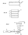
- the structure includes a layer of an amorphous crystallizable material 12 and a layer of a crystallization inhibiting material 14.
- the amorphous crystallizable material 12 is a material which is capable of existing in either the crystalline or amorphous state and which may be switched from one state to another by the application of the proper form and amount of energy thereto.
- the temperature at which the amorphous form of the material forming the layer 12 is switched to the crystalline state is substantially elevated.
- the instant invention may be practiced with any such material.
- some of the materials which may be employed for the fabrication of the crystallizable layer 12 include: tellurium, selenium, germanium, arsenic, and silicon as well as alloys and other materials containing the aforementioned elements.
- alloys and other materials containing the aforementioned elements include: tellurium, selenium, germanium, arsenic, and silicon as well as alloys and other materials containing the aforementioned elements.
- element containing material and its equivalents are meant to refer to the pure form of the element as well as all compounds, mixtures, alloys, and molecular species which include the specified element.
- a crystallization inhibiting layer 14 Disposed in immediate contact with substantially all of the amorphous crystallizable layer 12 is a crystallization inhibiting layer 14. It is a notable feature of the instant invention that the presence of this layer 14 substantially raises the temperature at which the amorphous crystallizable layer 12 changes from the amorphous to the crystalline state.
- the crystallization inhibiting layer 14 may be formed from a wide variety of materials, the main criteria being that the material forming the layer 14 have a crystallization temperature (if amorphous) which is higher than the crystallization temperature of the material in the crystallizable layer 12; or, have a crystalline phase transition temperature (if cyrstalline) greater than the crystallization temperature of the crystallizable layer 12.
- crystallization inhibiting layers 14 include by way of illustration and not limitation: germanium based materials, silicon based materials and boron based materials. Among the materials having particular utility are: silicon oxides, silicon nitrides, germanium oxides, germanium nitrides, silicate glasses, borosilcate glasses and combinations of the foregoing.
- the thickness of the inhibiting layer 14 is not critical to the instant invention. Any continuous layer of inhibiting material will exert its effect upon the crystallizable material. It has been determined experimentally that inhibition of crystallization may be obtained with layers as thin as 5 Angstroms.
- the crystallization inhibiting layer 14 may be a relatively thick member which also functions as a substrate for supporting and rigidifying the entire structure 10.
- amorphous germanium normally crystallizes when maintained at 400°C for approximately one hour.
- a layer of a crystallization inhibiting material such as silicon nitride, it may be maintained at temperatures of up to 600°C for one hour without crystallization.
- This micromechanical effect may result from a constraining of the constituent atoms of the amorphous matrix of the crystallizable layer 12, by the atoms of the inhibiting layer 14. This constraint prevents the atomic rearrangements necessary to effect crystallization.
- the micromechanical effect may occur through interactions between the atoms of the layers, and in this manner serves to increase the energy barrier separating the amorphous and the crystalline states. It has been noted that retardation of crystallization is not dependent on any alloying or mixing of the components of the two layers. Raman Spectroscopy has demonstrated that a distinct interface is obtained between the two layers and no difusion or intermixing occurs until crystallization temperature is reached, if it occurs at all,
- the multilayered structure 20 is generally similar in composition and dimensions to the structure 10 depicted with reference to Figure lA, except that it includes a plurality of amorphous crystallizable layers 12 and a plurality of crystallization inhibiting layers 14 disposed in alternating, generally coextensive relationship.
- the layers 12, 14 are generally similar to those described with reference to Figure 1A.
- the multilayered structure 20 of Figure 18 may be fabricated with layers of crystallizable material 12 which are all of substantially similar composition, or with layers of differing composition.
- the layers of crystallization inhibiting material 14 may be of similar or diverse composition.
- the component layers of the multilayered structure of the instant invention may be prepared by any one of the many techniques available to those skilled in the art, the instant invention not being limited by the method or manner employed for preparation of the layers.
- vacuum deposition techniques such as: sputtering, glow discharge deposition, evaporation, molecular beam epitaxy, ion plating, low pressure chemical vapor deposition and variants thereupon.
- Non-vacuum techniques such as electroplating, atmospheric pressure chemical vapor deposition, plasma spraying and the like may be employed.
- the only requirement for the apparatus and/or technique employed in the practice of the instant invention is that it be capable of providing uniform layers of material with distinct interfaces therebetween.
- the apparatus of Figure 2 is a modified ion-milling apparatus.
- the apparatus includes a source of ions such as an ion gun 22.
- Ion guns are well known to those skilled in the art and generally comprise an ion generating portion wherein atoms or molecules of a working medium, typically an inert gas such as argon, are ionized; the gun further includes an accelerating section in which the ionized material is kinetically energized and projected outward.
- a target 26 disposed so as to intercept the ion beam 24.
- the target 26 is generally maintained at ground potential and has at least a deposition surface 28 thereupon comprised of the material to be deposited, i.e., either the crystallizable material or the crystallization inhibiting material.
- the target 26 is disposed so as to present the deposition surface 28 in the path of the ion beam 24. When the deposition material 28 is thus disposed it will be struck by the ion beam 24 and a stream 32 of particles of the deposition material will be ejected from the target 26.
- An electrically grounded substrate member 30 is disposed so as to intercept the stream of ejected particles 32 and accumulate a deposit thereof thereupon.
- the deposition apparatus of Figure 2 is enclosed within an evacuable chamber so as to allow operation of the process at rressures below atmospheric.
- the target 26 and the substrate 30 may each have heating and/or cooling means associated therewith to maintain proper temperatures during the deposition process. Heating or cooling may be accomplished by any method well known to those skilled in the art of vacuum deposition.
- a substrate 30 is loaded into the apparatus.
- the substrate forms a support member for the multilayered structure.
- the substrate may itself be the crystallization inhibiting layer in which case the crystallizable material will be deposited directly thereupon.
- a layer of crystallization inhibiting material will be deposited upon the substrate.
- a target 26 Positioned in the apparatus is a target 26 having a deposition surface 28 formed of the first material to be deposited upon the substrate. For example, if a crystallization inhibiting layer of silicon nitride is to be the first deposited layer, the target 26 will have a surface 28 formed of bulk silicon nitride material.
- the vacuum system is activated to reduce the pressure within the apparatus to a working range, typically 10-4 torr.
- a stream of working gas such as argon is flowed into the ion gun 22 for production of an energetic beam 24 of argon ions.
- the ions impact upon the silicon nitride surface of the target 26 and emit a shower of silicon and nitrogen containing species in a stream 32 which strikes and condenses upon the substrate 30.
- the efficacy of the nitride layer in preventing crystallization was assessed by isochronally annealing the samples at progressively higher temperatures. Annealing in all cases was carried out for one hour after which time the samples were inspected for signs of crystallization. It was found that the unprotected germanium layer was completely crystallized after one hour of annealing at 400°C, while the germanium in the remaining layered samples was still amorphous. The layered samples were next annealed at 500°C for one hour. Inspection of the samples revealed no signs of crystallization.
- the five samples were next heated for one hour at 600°C. At the end of this time it was found that the sample having-a 5 Angstrom thick silicon nitride layers was completely crystallized, while the remaining samples showed progressively less crystallization as the thickness of the nitride layer increased.
- the sample having a 15 Angstrom thick protective layers was approximately 20% crystalline, the sample having the 50 Angstrom thick layers was approximately 20% crystalline and the sample having the 150 Angstrom thick protective layers was less than 20% crystalline.
- Germanium layers of 50, 100, 150 and 200 Angstroms thickness were evaporated under ultra high vacuum conditions, ie . approximately 10 -10 Torr.
- the first annealing run was made at 400 o C for one hour (ie, the approximate bulk crystallization temperature for evaporated or sputtered germanium). It was noted that the 200 Angstrom thick sample began to crystallize under these conditions; less than 5% crystallites were present in the sample. The thinner samples all remained in the amorphous state. The samples were next annealed at 460°C for one hour. The 200 Angstrom thick sample crystallized completely under these conditions and the 150 Angstroms thick sample began to crystallize. The 100 Angstrom and the 50 Angstrom thick samples remained amorphous. The samples were next annealed at 500°C for one hour. The 150 Angstrom thick sample was completely crystalline. The 100 Angstrom thick sample was approximately 20% crystalline while the 50 Angstrom thick sample remained amorphous.
- the effect of a layer of silicon nitride in retarding the crystallization of a layer of silicon was assessed.
- the various layers for this experimental series were prepared by radio frequency energized glow discharge deposition, as is well known to those skilled in the art.
- the silicon layers were deposited from a gas mixture which included silane and accordingly are amorphous silicon:hydrogen alloy layers.
- the nitride layers were deposited from a gas mixture which incuded silane and ammonia and accordingly are amorphous silicon:hydrogen:nitrogen alloy layers. It has been found that bulk amorphous silicon:hydrogen material prepared under these conditions crystallizes at approximately 650°C.
- a first sample was prepared which comprised ten layers of amorphous silicon:hydrogen material of approximately 20 Angstroms and 10 layers of amorphous silicon:hydrogen:nitrogen alloy material also of approximately 20 Angstroms, disposed in alternating relationship so as to yield a 20 layer structure.
- the thus prepared sample was annealed at 900°C for one hour. Analysis via Raman Spectroscopy showed that approximately 3% of the silicon:hydrogen alloy material had crystallized.
- a second sample was prepared which was generally similar to the first sample except that the silicon:hydrogen alloy layers were.40 Angstroms thick. This sample was annealed at 800°C for one hour and it was found that the silicon:hydrogen alloy layers were approximately 20% crystalline.
- the instant invention provides for the retardation of the crystallization of a layer of material to temperatures significantly above the normal bulk crystallization temperature thereof.
- the instant invention accordingly has significant utility in the fabrication of optical memory media wherein data is stored by changing the phase of a portion of a layer of material.
- the crystallization transition temperature of the material may be changed without producing any change in the bulk property thereof. This ability is useful in cases where it is desired to utilize an unstable material as a storage medium.
- phase change storage layer insofar as an unstable material will give a quick switching or setting time; however, unstable materials generally have a low crystallization temperature and may be inadvertantly set or switched during handling.
- unstable materials generally have a low crystallization temperature and may be inadvertantly set or switched during handling.
- the instant invention also has utility in the manufacture of light absorbing layers for photothermal energy conversion. It has been found that some amorphous materials have high optical absorption coefficients making them particularly suited as absorbing members for converting light to heat. However, heating can crystallize such layers, and thereby change their optical properties. Accordingly, the temperature range over which they may be employed is restricted. The addition of alloying agents can retard crystallization, however such agents also change the optical absorption of the material. By employing the principles disclosed herein, the crystallization temperature of the amorphous layer may be raised without effecting any change in the optical properties thereof.
Landscapes
- Chemical & Material Sciences (AREA)
- Inorganic Chemistry (AREA)
- Physics & Mathematics (AREA)
- General Physics & Mathematics (AREA)
- Physical Vapour Deposition (AREA)
- Laminated Bodies (AREA)
Applications Claiming Priority (2)
| Application Number | Priority Date | Filing Date | Title |
|---|---|---|---|
| US73429385A | 1985-05-15 | 1985-05-15 | |
| US734293 | 1985-05-15 |
Publications (2)
| Publication Number | Publication Date |
|---|---|
| EP0201860A2 true EP0201860A2 (de) | 1986-11-20 |
| EP0201860A3 EP0201860A3 (en) | 1989-02-15 |
Family
ID=24951078
Family Applications (1)
| Application Number | Title | Priority Date | Filing Date |
|---|---|---|---|
| EP86106237A Ceased EP0201860A3 (en) | 1985-05-15 | 1986-05-07 | Multilayered article including crystallization inhibiting layer and method for fabricating same |
Country Status (3)
| Country | Link |
|---|---|
| EP (1) | EP0201860A3 (de) |
| JP (1) | JPS61280927A (de) |
| CA (1) | CA1272666A (de) |
Cited By (5)
| Publication number | Priority date | Publication date | Assignee | Title |
|---|---|---|---|---|
| EP0449121A3 (en) * | 1990-03-27 | 1992-08-05 | Fuji Photo Film Co., Ltd. | Optical recording medium and recording/reproducing method therefor |
| EP0936605A1 (de) * | 1998-02-10 | 1999-08-18 | Sony Corporation | Optisches Speichermedium und Herstellungsverfahren |
| WO2000022618A1 (fr) * | 1998-10-09 | 2000-04-20 | Commissariat A L'energie Atomique | Support d'enregistrement optique et procede de realisation de ce support |
| WO2009115995A1 (en) * | 2008-03-21 | 2009-09-24 | Nxp B.V. | An electronic component comprising a convertible structure |
| CN110941107A (zh) * | 2018-09-21 | 2020-03-31 | 三星电子株式会社 | 多层薄膜结构和使用多层薄膜结构的相移器件 |
Family Cites Families (3)
| Publication number | Priority date | Publication date | Assignee | Title |
|---|---|---|---|---|
| US3778785A (en) * | 1972-04-20 | 1973-12-11 | Ibm | Method for writing information at nanosecond speeds and a memory system therefor |
| EP0045183B1 (de) * | 1980-07-25 | 1984-12-05 | Asahi Kasei Kogyo Kabushiki Kaisha | Aufzeichnungsmaterial |
| US4433342A (en) * | 1981-04-06 | 1984-02-21 | Harris Corporation | Amorphous switching device with residual crystallization retardation |
-
1986
- 1986-05-05 CA CA000508426A patent/CA1272666A/en not_active Expired - Lifetime
- 1986-05-07 EP EP86106237A patent/EP0201860A3/en not_active Ceased
- 1986-05-14 JP JP61110453A patent/JPS61280927A/ja active Pending
Cited By (7)
| Publication number | Priority date | Publication date | Assignee | Title |
|---|---|---|---|---|
| EP0449121A3 (en) * | 1990-03-27 | 1992-08-05 | Fuji Photo Film Co., Ltd. | Optical recording medium and recording/reproducing method therefor |
| EP0936605A1 (de) * | 1998-02-10 | 1999-08-18 | Sony Corporation | Optisches Speichermedium und Herstellungsverfahren |
| US6194046B1 (en) | 1998-02-10 | 2001-02-27 | Sony Corporation | Optical recording medium and manufacturing method thereof |
| WO2000022618A1 (fr) * | 1998-10-09 | 2000-04-20 | Commissariat A L'energie Atomique | Support d'enregistrement optique et procede de realisation de ce support |
| FR2785078A1 (fr) * | 1998-10-09 | 2000-04-28 | Commissariat Energie Atomique | Support d'enregistrement optique et procede de realisation de ce support |
| WO2009115995A1 (en) * | 2008-03-21 | 2009-09-24 | Nxp B.V. | An electronic component comprising a convertible structure |
| CN110941107A (zh) * | 2018-09-21 | 2020-03-31 | 三星电子株式会社 | 多层薄膜结构和使用多层薄膜结构的相移器件 |
Also Published As
| Publication number | Publication date |
|---|---|
| EP0201860A3 (en) | 1989-02-15 |
| JPS61280927A (ja) | 1986-12-11 |
| CA1272666A (en) | 1990-08-14 |
Similar Documents
| Publication | Publication Date | Title |
|---|---|---|
| US4792501A (en) | Multilayered article including crystallization inhibiting layer and method for fabricating same | |
| Martin | Ion-based methods for optical thin film deposition | |
| Musil et al. | Magnetron sputtering of films with controlled texture and grain size | |
| Mohan et al. | A review of ion beam assisted deposition of optical thin films | |
| EP0896553B1 (de) | Optisches aufzeichungsmedium mit mehreren diskreten punkten zur aufnahme von phasenanderungsdaten | |
| Thornton et al. | Stress-related effects in thin films | |
| Maruyama et al. | Copper nitride and tin nitride thin films for write‐once optical recording media | |
| Pawlewicz et al. | Recent developments in reactively sputtered optical thin films | |
| WO2000004575A3 (en) | Collimated sputtering of semiconductor and other films | |
| GB2433647A (en) | Phase change memory materials | |
| Geetha Priyadarshini et al. | Structural and morphological investigations on DC-magnetron-sputtered nickel films deposited on Si (100) | |
| Mehta | Overview of coating deposition techniques | |
| Lie et al. | Ge2Sb2Te5 thin film doped with silver | |
| CA1272666A (en) | Multilayered article including crystallization inhibiting layer and method for fabricating same | |
| US20040040837A1 (en) | Method of forming chalcogenide sputter target | |
| US4649024A (en) | Method for forming evaporated pnictide and alkali metal polypnictide films | |
| Awan et al. | Role of Thin Film in Deposition Techniques | |
| US8206804B2 (en) | Phase change memory materials | |
| Vincett | Critical optimization | |
| Kaiser | Some fundamentals of optical thin film growth | |
| US12559834B2 (en) | Thermally stable metallic glass films via steep compositional gradients | |
| Chou | Thin binary In1− xSbx films prepared by flash evaporation | |
| Macleod | Ion and photon-beam assisted deposition of thin films | |
| Takagi et al. | Ionized-cluster-beam deposition of optical interference coatings | |
| JPH0399884A (ja) | 情報記録媒体 |
Legal Events
| Date | Code | Title | Description |
|---|---|---|---|
| PUAI | Public reference made under article 153(3) epc to a published international application that has entered the european phase |
Free format text: ORIGINAL CODE: 0009012 |
|
| AK | Designated contracting states |
Kind code of ref document: A2 Designated state(s): AT BE CH DE FR GB IT LI LU NL SE |
|
| PUAL | Search report despatched |
Free format text: ORIGINAL CODE: 0009013 |
|
| AK | Designated contracting states |
Kind code of ref document: A3 Designated state(s): AT BE CH DE FR GB IT LI LU NL SE |
|
| 17P | Request for examination filed |
Effective date: 19890228 |
|
| 17Q | First examination report despatched |
Effective date: 19910304 |
|
| STAA | Information on the status of an ep patent application or granted ep patent |
Free format text: STATUS: THE APPLICATION HAS BEEN REFUSED |
|
| 18R | Application refused |
Effective date: 19920127 |
|
| RIN1 | Information on inventor provided before grant (corrected) |
Inventor name: ALLRED, DAVID D., PH. D. PHYSICS Inventor name: GONZALEZ-HERNANDEZ, JESUS, PH. D. PHYSICS Inventor name: VAN NGUYEN, ON |