EP0201862A2 - Rangée de lentilles en matière plastique - Google Patents
Rangée de lentilles en matière plastique Download PDFInfo
- Publication number
- EP0201862A2 EP0201862A2 EP86106241A EP86106241A EP0201862A2 EP 0201862 A2 EP0201862 A2 EP 0201862A2 EP 86106241 A EP86106241 A EP 86106241A EP 86106241 A EP86106241 A EP 86106241A EP 0201862 A2 EP0201862 A2 EP 0201862A2
- Authority
- EP
- European Patent Office
- Prior art keywords
- convex lenses
- image
- lens array
- lenses
- convex
- Prior art date
- Legal status (The legal status is an assumption and is not a legal conclusion. Google has not performed a legal analysis and makes no representation as to the accuracy of the status listed.)
- Granted
Links
Images



Classifications
-
- G—PHYSICS
- G02—OPTICS
- G02B—OPTICAL ELEMENTS, SYSTEMS OR APPARATUS
- G02B17/00—Systems with reflecting surfaces, with or without refracting elements
- G02B17/08—Catadioptric systems
- G02B17/0856—Catadioptric systems comprising a refractive element with a reflective surface, the reflection taking place inside the element, e.g. Mangin mirrors
- G02B17/086—Catadioptric systems comprising a refractive element with a reflective surface, the reflection taking place inside the element, e.g. Mangin mirrors wherein the system is made of a single block of optical material, e.g. solid catadioptric systems
-
- G—PHYSICS
- G02—OPTICS
- G02B—OPTICAL ELEMENTS, SYSTEMS OR APPARATUS
- G02B17/00—Systems with reflecting surfaces, with or without refracting elements
- G02B17/002—Arrays of reflective systems
-
- G—PHYSICS
- G02—OPTICS
- G02B—OPTICAL ELEMENTS, SYSTEMS OR APPARATUS
- G02B17/00—Systems with reflecting surfaces, with or without refracting elements
- G02B17/008—Systems specially adapted to form image relays or chained systems
-
- G—PHYSICS
- G02—OPTICS
- G02B—OPTICAL ELEMENTS, SYSTEMS OR APPARATUS
- G02B3/00—Simple or compound lenses
- G02B3/0006—Arrays
- G02B3/0037—Arrays characterized by the distribution or form of lenses
- G02B3/0062—Stacked lens arrays, i.e. refractive surfaces arranged in at least two planes, without structurally separate optical elements in-between
- G02B3/0068—Stacked lens arrays, i.e. refractive surfaces arranged in at least two planes, without structurally separate optical elements in-between arranged in a single integral body or plate, e.g. laminates or hybrid structures with other optical elements
Definitions
- the present invention relates to a lens array for forming an erect image of unit magnification and adopted in document reading or in image formation for a copying machine, a printer, a facsimile, etc.
- An LED type recording apparatus or a liquid crystal type recording apparatus includes a photosensitive drum, around which are arranged a uniformly charging portion, an image forming portion, a developing portion, a transferring portion, a cleaning portion, an electric discharging portion, etc.
- a photosensitive drum around which are arranged a uniformly charging portion, an image forming portion, a developing portion, a transferring portion, a cleaning portion, an electric discharging portion, etc.
- an image corresponding to an image to be recorded is formed on the photosensitive drum by means of an LED array or a liquid crystal.
- a light guiding lens array is used.
- a document reading device adopted for a facsimile, etc. detects by means of an image sensor, etc., the light which is emitted from LEDs and reflected from a document, and converts the detected light into electric image signals.
- the light guiding lens array is used.
- An electrographic plain paper copying machine includes a photosensitive drum, around which, similar to the above recording apparatus, are arranged a uniformly charging portion, an image forming portion, a developing portion, a transferring portion, a cleaning portion, an electric discharging portion, etc.
- a uniformly charging portion At the image forming portion, an original to be copied is irradiated with the light to form an image corresponding to the document on the photosensitive drum by virtue of the light reflected from the document.
- the light guiding lens array is used.
- the present invention is applicable to such a light guiding lens array adopted for the recording apparatus, document reading apparatus, copying machine, etc.
- a prior art lens array structure is disclosed in, for instance, the publication of Japanese Patent Application No. 58-86515.
- This lens array comprises two kinds of Porro prisms which are right-and-left symmetrical and continuously combined one after another.
- Each Porro prism comprises three rectangular prisms, in which a bottom surface of a first rectangular prism is in contact with second and third rectangular prisms in such a manner that bottom surfaces of the second and third rectangular prisms will face upward and downward respectively.
- Convex tenses are provided under a lower surface of the second rectangular prism and on an upper surface of the third rectangular prism respectively. According to this arrangement, the incident light from an object into one of the convex lenses is radiated out of the other convex lens to form an erected real image of the object,
- This lens array structure comprises a plurality of solidly formed lens elements which are arranged continuously.
- Each of the solidly formed lens elements has a par of convex lens surfaces having a common optical axis; another pair of convex lens surfaces having respective optical axes orthogonal to the common optical axis; and a pair of reflecting surfaces formed inside the two pairs of convex lens surfaces.
- the reflecting surfaces are coated with metallic reflective films. According to this arrangement, the incident light from an object into one of the convex lens surfaces having the common optical axis is radiated out of the other convex tens surface to form an erect image of unit magnification of the object.
- an angle of a rejecting surface of the prism is restricted to 45 with respect to an optical axis.
- a light receiving area of the prism in which the light may be totally reffefiected with an angle exceeding a critical angle, is limited to a narrow region, and the light from other than this narrow region is not reflected by the prism but passes through the prism so that the light radiated from the prism will become dark.
- each lens element must be coated with reflective film so that the number of manufacturing processes is increased. Further, the lens elements must be arranged and engaged in an array that will require more time for assembling and thus deteriorate the productivity.
- the present invention provides a plastic lens array comprising the following members which are formed integrally as one block by a plastic material:
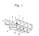
- FIG. 1 is a perspective view showing an embodiment according to the present invention.
- a plurality of object convex lenses 4 are arranged side by side in a row along one side of an array body member 7.
- a plurality of image convex lenses 5 corresponding to the object convex lenses 4.
- roof members 6 are provided at the bottom of the array body member 7.
- Each of the roof members 6 comprises a pair of roof surfaces 6a and 6b which are substantially normal to each other.
- the roof members 6 are arranged in parallel with one another in such a manner that each of the roof members 6 corresponds to a pair of the object and image lenses 4 and 5.
- a V-groove 3 is formed at the top of the array body member 7.
- the V-groove 3 is formed along a longitudinal axis of the array body member 7, namely, along the rows of lenses 4 and 5. Slant side faces of the V-groove 3 are located at the backs of the object and image convex lenses 4 and 5, respectively, to constitute a first reflecting surface I and a second reflecting surface 2, respectively.
- the object convex lenses 4, image convex lenses 5, and roof members 6 are made simultaneously and integrally with the array body member 7 as one body by a plastic material by using a mold.
- the plastic material polymethyl methacrylate, polycarbonate, polystyrene, poly-4-methylpenten-1, etc., may be used.
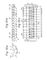
- Figs. 2 Such a lens array is shown in Figs. 2, in which Fig. 2(a) is a side view, Fig. 2(b) a front view, and Fig. 2(c) a bottom view.
- Angles e of the first reflecting surface and of the second reflecting surface 2 are formed in such a manner that the respective angles of perpendicular lines of the reflecting surfaces I and 2 with respect to optical axes of the lenses 4 and 5 excesd a critical angle.
- a corresponding pair of the object and image convex lenses 4 and 5 is coaxially arranged to have a common optical axis. In this coaxial arrangement, it is preferable to provide a gap G between adjacent lenses.
- the V-groove 3 is formed in such a manner that the top of V-groove 3 is positioned at the same level as the lower lines of lenses 4 and 5 or below, to make a sufficient and effective use of the entire diameter of each of the lenses 4 and 5.
- Each roof member 6 comprises two roof surfaces 6a and 6b which are substantially normal to each other.
- the light from the upper part (actually, from the oblique upper part) reaches one roof surface 6a, is reflected thereby, proceeds toward another roof surface 6b, and is again reflected upwardly (toward the oblique upper part on the other side).
- the image of an object is inverted and transmitted.
- Figure 4 shows optical paths in an image formation in the lens array shown in Fig. 2.
- the marks F and F indicate focal points of the object convex lens 4 and the image convex lens 5, respectively.
- the light from an object S enters the lens array through the object convex lens 4 and is totally reflected by the first reflecting surface 1 with an angle which exceeds a critical angle.
- the totally reflected light is inverted by the roof member 6 and proceeds toward the second reflecting surface 2.
- the light inverted by the roof member 6 is totally reflected by the second reflecting surface 2 with an angle which exceeds the critical angle.
- the light totally reflected by the second reflecting surface 2 is radiated out of the image convex lens 5 to form an erect image R at equal magnification.
- the first and second reflecting surfaces 1 and 2 are constituted in such a manner that the light from the object convex lens 4 and the light from the roof member 6 are totally reflected by the reflecting surfaces 1 and 2, respectively, each with an angle which exceeds the critical angle.
- coating of a eflective film is not required.
- an angle of the reflecting surface is not limited to 45° as required in the prior art
- a thin and compact lens array can be realized according to the present invention.
- optical paths which pass through a center cross section of each lens are shown to be inverted in the vicinity of the top of the roof member 6.
- Figure 7 is a graph showing the MTF of the lens array with respect to various angles 8 of the first and second reflecting surfaces and 2. As seen from the graph, the MTF takes the maximum value (92%) when the ⁇ is 30°.
- the measurment was made under the condition of 6 Ip/mm, and the lens array used in the experiment was of polymethyl methacrylate material and under the following conditions:
- FIG. 3 shows the constitution of another embodiment according to the present invention.
- This embodiment differs from the embodiment shown in Fig. 2 in that the optical axes of a pair of the object and image convex lenses 4 and 5 are dislocated relative to each other in a horizontal direction - (along the lens array).
- Each roof member 6 is located in the middle of the optical axes of each pair of the object and image convex lenses 4 and 5 in connection with the horizontal direction.
- most of the light through the object convex lens 4 is reflected by a central portion of the roof surface 6a, as indicated by an arrow r shown in Fig. 3(c), reflected further by a central portion of the roof surface 6b, and passed through the image convex lens 5. Therefore, the light to be inverted does not pass the top portion of the roof member 6. As a result, a good image can be obtained even if the manufacturing accuracy of the top portion is rough.
- Figure 5 is a view showing optical paths in the above embodiment of Fig. 3.
- the constitution, action, and effect of the above embodiment other than the above-mentioned difference are the same as those of the embodiment shown in Fig. 2.
- Figure 8 shows still another embodiment according to the present invention.
- This embodiment is substantially the same as the embodiment shown in Fig. 3, but differs therefrom in that adjacent lenses in the row of object convex lenses 4 and in the row of image convex lenses 5 are formed so that they are almost in contact with each other.
- the optical axis of each object convex lens 4 and the optical axis of each image convex lens 5 are dislocated with respect to each other, the optical interference between the adjacent lenses is minimized, and a good image is obtained even if a gap is not provided between the adjacent lenses. According to the above arrangement, a compact lens array can be obtained.
- the constitution, action, and effect of this embodiment other than the above-mentioned difference are the same as those of the embodiment shown in Fig. 3.
- Figure 9 shows still another embodiment according to the present invention.
- the lens array is divided into two groups, i.e., a left half group and a right half group.
- the optical axes of the image convex lenses 5a and 5b are dislocated outwardly (toward outer ends of the array body member) relative to the optical axes of the object convex lenses 4a and 4b, respectively.
- Fig. 1 the optical axes of the image convex lenses 5a and 5b are dislocated outwardly (toward outer ends of the array body member) relative to the optical axes of the object convex lenses 4a and 4b, respectively.
- each image convex lens 5a in the right half lens group, the optical axis of each image convex lens 5a is dislocated rightwardly relative to the optical axis of each object convex lens 4a, and in the left half lens group, the optical axis of each image convex lens 5b is dislocated leftwardly relative to the optical axis of each object convex lens 4b.
- a single document 8 can be read by using two CCD image sensors 9a and 9b.
- the CCD image sensors which are manufactured from silicon wafers are limited in their dimensions, and therefore, a gap may be formed between two CCD image sensors when they are arranged in the device. In spite of the existence of such a gap, the original can be continuously read according to this embodiment. As a result, a large sized document can be read.
- FIG 10 shows still another embodiment according to the present invention.
- a lens array is divided into three groups.
- the optical axes of image convex lenses 5a and 5b are dislocated outwardly relative to the optical axes of object convex lenses 4a and 4b respectively, while in a middle group, the optical axes of each image convex lens 5c and each object convex lens 4c coincide with each other.
- CCD image sensors 9a, 9b and 9c are arranged on the side of image convex lenses 5a, 5b, and 5c to correspond to the three groups, respectively.
- a single original 8 provided on the side of object convex lenses 4a, 4b, and 4c can be read by using three CCD image sensors 9a, 9b, and 9c so that a larger original can be read in comparison with the embodiment shown in Fig. 9.
- Figure 11 shows another embodiment according to the present invention.
- array fitting pieces 10 projecting outwardly from both ends of the array body member 7 are integrally formed with the array body member 7. According to this arrangement, the lens array may be easily assembled for a reading device, etc., due to the provision of solidly formed fitting pieces 0 having no dispersion in accuracy, and the uniformity of products can be maintained.
Landscapes
- Physics & Mathematics (AREA)
- General Physics & Mathematics (AREA)
- Optics & Photonics (AREA)
- Lenses (AREA)
- Facsimile Heads (AREA)
Applications Claiming Priority (6)
| Application Number | Priority Date | Filing Date | Title |
|---|---|---|---|
| JP9855185 | 1985-05-09 | ||
| JP98551/85 | 1985-05-09 | ||
| JP14162385 | 1985-06-28 | ||
| JP141623/85 | 1985-06-28 | ||
| JP61094840A JPS6296924A (ja) | 1985-05-09 | 1986-04-25 | プラスチツクレンズアレイ |
| JP94840/86 | 1986-04-25 |
Publications (3)
| Publication Number | Publication Date |
|---|---|
| EP0201862A2 true EP0201862A2 (fr) | 1986-11-20 |
| EP0201862A3 EP0201862A3 (en) | 1988-07-06 |
| EP0201862B1 EP0201862B1 (fr) | 1992-08-12 |
Family
ID=27307664
Family Applications (1)
| Application Number | Title | Priority Date | Filing Date |
|---|---|---|---|
| EP86106241A Expired - Lifetime EP0201862B1 (fr) | 1985-05-09 | 1986-05-07 | Rangée de lentilles en matière plastique |
Country Status (3)
| Country | Link |
|---|---|
| US (1) | US4747667A (fr) |
| EP (1) | EP0201862B1 (fr) |
| DE (1) | DE3686348T2 (fr) |
Cited By (4)
| Publication number | Priority date | Publication date | Assignee | Title |
|---|---|---|---|---|
| EP0394867A3 (fr) * | 1989-04-28 | 1991-02-06 | AT&T Corp. | Appareil télautographique à optique intégrée |
| EP2455783A1 (fr) * | 2010-11-18 | 2012-05-23 | Pixon Technologies Corp. | Lentille à prisme Abbe à focalisation améliorée et lumière parasite réduite |
| CN102466824A (zh) * | 2010-11-18 | 2012-05-23 | 景传光电股份有限公司 | 透镜和透镜数组 |
| TWI476443B (zh) * | 2010-11-18 | 2015-03-11 | Pixon Technologies Corp | 具有改良式焦點與降低雜散光之阿貝稜鏡式透鏡 |
Families Citing this family (10)
| Publication number | Priority date | Publication date | Assignee | Title |
|---|---|---|---|---|
| US4917461A (en) * | 1989-01-11 | 1990-04-17 | Goldstein Dennis H | Achromatic infrared retarder |
| US5245175A (en) * | 1989-12-28 | 1993-09-14 | Olympus Optical Co., Ltd. | Focus detecting optical system including a plurality of focus blocks composed of an integrally molded prism member |
| JP3890128B2 (ja) * | 1997-10-28 | 2007-03-07 | 沖電気工業株式会社 | 反射型プリズム |
| US6342981B1 (en) * | 1999-09-21 | 2002-01-29 | Rose Research, Llc | Zero-displacement phase retarder device and method |
| US7167615B1 (en) | 1999-11-05 | 2007-01-23 | Board Of Regents, The University Of Texas System | Resonant waveguide-grating filters and sensors and methods for making and using same |
| AU2001245787A1 (en) | 2000-03-17 | 2001-10-03 | Zograph, Llc | High acuity lens system |
| KR100674711B1 (ko) | 2005-12-28 | 2007-01-25 | 삼성전기주식회사 | 모바일 카메라 광학계의 광학 렌즈 시스템 |
| DE102010014099A1 (de) * | 2010-04-07 | 2011-10-13 | Siteco Beleuchtungstechnik Gmbh | Leuchte mit Abdeckscheibe |
| AU2016433012B2 (en) * | 2016-12-23 | 2022-02-03 | Chongqing Hylon Co., Ltd. | Composite prism for multi-functional telescope, and binocular telescopic optical system for same |
| JP2020148959A (ja) * | 2019-03-14 | 2020-09-17 | トヨタ自動車株式会社 | 光学デバイス |
Family Cites Families (8)
| Publication number | Priority date | Publication date | Assignee | Title |
|---|---|---|---|---|
| US3449158A (en) * | 1963-02-27 | 1969-06-10 | Rowland Products Inc | Method of making a phased lenticular composite strip for optical effects |
| US3360323A (en) * | 1963-10-07 | 1967-12-26 | Electro Optical Systems Inc | Transverse magneto-optical rotator with compensation of phase retardation |
| US3514182A (en) * | 1967-11-06 | 1970-05-26 | Ibm | Light focus shifting system |
| FR1565507A (fr) * | 1968-02-20 | 1969-05-02 | ||
| US3544190A (en) * | 1968-11-29 | 1970-12-01 | Xerox Corp | Lens strip optical scanning system |
| US3836249A (en) * | 1972-09-13 | 1974-09-17 | Bell & Howell Co | Optical imaging system of short focal lens |
| FR2266897B1 (fr) * | 1974-04-03 | 1978-04-21 | Instruments Sa | |
| JPS5886515A (ja) * | 1981-11-18 | 1983-05-24 | Ricoh Co Ltd | 小型結像光学系 |
-
1986
- 1986-05-07 DE DE8686106241T patent/DE3686348T2/de not_active Expired - Fee Related
- 1986-05-07 US US06/860,483 patent/US4747667A/en not_active Expired - Lifetime
- 1986-05-07 EP EP86106241A patent/EP0201862B1/fr not_active Expired - Lifetime
Cited By (4)
| Publication number | Priority date | Publication date | Assignee | Title |
|---|---|---|---|---|
| EP0394867A3 (fr) * | 1989-04-28 | 1991-02-06 | AT&T Corp. | Appareil télautographique à optique intégrée |
| EP2455783A1 (fr) * | 2010-11-18 | 2012-05-23 | Pixon Technologies Corp. | Lentille à prisme Abbe à focalisation améliorée et lumière parasite réduite |
| CN102466824A (zh) * | 2010-11-18 | 2012-05-23 | 景传光电股份有限公司 | 透镜和透镜数组 |
| TWI476443B (zh) * | 2010-11-18 | 2015-03-11 | Pixon Technologies Corp | 具有改良式焦點與降低雜散光之阿貝稜鏡式透鏡 |
Also Published As
| Publication number | Publication date |
|---|---|
| US4747667A (en) | 1988-05-31 |
| DE3686348D1 (de) | 1992-09-17 |
| EP0201862A3 (en) | 1988-07-06 |
| EP0201862B1 (fr) | 1992-08-12 |
| DE3686348T2 (de) | 1993-02-11 |
Similar Documents
| Publication | Publication Date | Title |
|---|---|---|
| EP0201862A2 (fr) | Rangée de lentilles en matière plastique | |
| EP0461660B1 (fr) | Lentille F-Theta et appareil de formation d'image et son utilisation | |
| US5035486A (en) | Optical imaging apparatus | |
| US5838504A (en) | Prism and real image type view finder | |
| US10054790B2 (en) | Imaging optical system | |
| US4992818A (en) | Focus detecting device | |
| US4561730A (en) | Synthetic resin lens system for imaging apparatus | |
| US5907438A (en) | Imaging device | |
| EP0809814B1 (fr) | Reseau de lentilles a largeur arbitraire avec champ d'image s'etendant sur toute la largeur d'un substrat | |
| US4512641A (en) | Compound eye projection device | |
| US20080225365A1 (en) | Optical scanning device and image forming apparatus using the device | |
| US20060055996A1 (en) | Beam scanning device with light blocking member | |
| US4878078A (en) | Focus detecting device and method of making same | |
| US4505570A (en) | Image-forming optical system | |
| KR900001118B1 (ko) | 플라스틱 렌즈 배열 | |
| JPS61226701A (ja) | レンズアレイ | |
| US4427291A (en) | Compact optical imaging apparatus | |
| JPS6296924A (ja) | プラスチツクレンズアレイ | |
| US4357099A (en) | Optical imaging system | |
| JPH0222361B2 (fr) | ||
| JP7188006B2 (ja) | 光書込装置、および画像形成装置 | |
| JPS58219542A (ja) | 光学像投影装置 | |
| JP2026043743A (ja) | レンズアレイユニット及び画像読取装置 | |
| JP3034757B2 (ja) | ルーフミラーレンズアレイ | |
| JPH01243009A (ja) | 焦点検出装置 |
Legal Events
| Date | Code | Title | Description |
|---|---|---|---|
| PUAI | Public reference made under article 153(3) epc to a published international application that has entered the european phase |
Free format text: ORIGINAL CODE: 0009012 |
|
| AK | Designated contracting states |
Kind code of ref document: A2 Designated state(s): DE FR GB NL |
|
| RIN1 | Information on inventor provided before grant (corrected) |
Inventor name: HARA, TOSHITO Inventor name: TERASHIMA, MINORU Inventor name: TANAKA, MASAO Inventor name: TAKAHASHI, EIETSU Inventor name: TANAKA, AKIRA |
|
| PUAL | Search report despatched |
Free format text: ORIGINAL CODE: 0009013 |
|
| AK | Designated contracting states |
Kind code of ref document: A3 Designated state(s): DE FR GB NL |
|
| RIN1 | Information on inventor provided before grant (corrected) |
Inventor name: HARA, TOSHITO Inventor name: TERASHIMA, MINORU Inventor name: TANAKA, MASAO Inventor name: TAKAHASHI, EIETSU Inventor name: TANAKA, AKIRA |
|
| 17P | Request for examination filed |
Effective date: 19880903 |
|
| 17Q | First examination report despatched |
Effective date: 19901206 |
|
| GRAA | (expected) grant |
Free format text: ORIGINAL CODE: 0009210 |
|
| AK | Designated contracting states |
Kind code of ref document: B1 Designated state(s): DE FR GB NL |
|
| PGFP | Annual fee paid to national office [announced via postgrant information from national office to epo] |
Ref country code: FR Payment date: 19920828 Year of fee payment: 8 |
|
| REF | Corresponds to: |
Ref document number: 3686348 Country of ref document: DE Date of ref document: 19920917 |
|
| ET | Fr: translation filed | ||
| PGFP | Annual fee paid to national office [announced via postgrant information from national office to epo] |
Ref country code: GB Payment date: 19930427 Year of fee payment: 8 |
|
| PLBE | No opposition filed within time limit |
Free format text: ORIGINAL CODE: 0009261 |
|
| STAA | Information on the status of an ep patent application or granted ep patent |
Free format text: STATUS: NO OPPOSITION FILED WITHIN TIME LIMIT |
|
| 26N | No opposition filed | ||
| PG25 | Lapsed in a contracting state [announced via postgrant information from national office to epo] |
Ref country code: GB Effective date: 19940507 |
|
| GBPC | Gb: european patent ceased through non-payment of renewal fee |
Effective date: 19940507 |
|
| PG25 | Lapsed in a contracting state [announced via postgrant information from national office to epo] |
Ref country code: FR Effective date: 19950131 |
|
| REG | Reference to a national code |
Ref country code: FR Ref legal event code: ST |
|
| PGFP | Annual fee paid to national office [announced via postgrant information from national office to epo] |
Ref country code: NL Payment date: 20020529 Year of fee payment: 17 |
|
| PG25 | Lapsed in a contracting state [announced via postgrant information from national office to epo] |
Ref country code: NL Free format text: LAPSE BECAUSE OF NON-PAYMENT OF DUE FEES Effective date: 20031201 |
|
| NLV4 | Nl: lapsed or anulled due to non-payment of the annual fee |
Effective date: 20031201 |
|
| PGFP | Annual fee paid to national office [announced via postgrant information from national office to epo] |
Ref country code: DE Payment date: 20040520 Year of fee payment: 19 |
|
| PG25 | Lapsed in a contracting state [announced via postgrant information from national office to epo] |
Ref country code: DE Free format text: LAPSE BECAUSE OF NON-PAYMENT OF DUE FEES Effective date: 20051201 |