EP0202108A2 - Couches intermédiaires à base de silanols contenant du phosphore et du bore dans la fabrication de films diélectriques - Google Patents
Couches intermédiaires à base de silanols contenant du phosphore et du bore dans la fabrication de films diélectriques Download PDFInfo
- Publication number
- EP0202108A2 EP0202108A2 EP86303627A EP86303627A EP0202108A2 EP 0202108 A2 EP0202108 A2 EP 0202108A2 EP 86303627 A EP86303627 A EP 86303627A EP 86303627 A EP86303627 A EP 86303627A EP 0202108 A2 EP0202108 A2 EP 0202108A2
- Authority
- EP
- European Patent Office
- Prior art keywords
- composition
- ratio
- zero
- essentially
- film
- Prior art date
- Legal status (The legal status is an assumption and is not a legal conclusion. Google has not performed a legal analysis and makes no representation as to the accuracy of the status listed.)
- Withdrawn
Links
Images


Classifications
-
- C—CHEMISTRY; METALLURGY
- C09—DYES; PAINTS; POLISHES; NATURAL RESINS; ADHESIVES; COMPOSITIONS NOT OTHERWISE PROVIDED FOR; APPLICATIONS OF MATERIALS NOT OTHERWISE PROVIDED FOR
- C09D—COATING COMPOSITIONS, e.g. PAINTS, VARNISHES OR LACQUERS; FILLING PASTES; CHEMICAL PAINT OR INK REMOVERS; INKS; CORRECTING FLUIDS; WOODSTAINS; PASTES OR SOLIDS FOR COLOURING OR PRINTING; USE OF MATERIALS THEREFOR
- C09D5/00—Coating compositions, e.g. paints, varnishes or lacquers, characterised by their physical nature or the effects produced; Filling pastes
-
- C—CHEMISTRY; METALLURGY
- C08—ORGANIC MACROMOLECULAR COMPOUNDS; THEIR PREPARATION OR CHEMICAL WORKING-UP; COMPOSITIONS BASED THEREON
- C08G—MACROMOLECULAR COMPOUNDS OBTAINED OTHERWISE THAN BY REACTIONS ONLY INVOLVING UNSATURATED CARBON-TO-CARBON BONDS
- C08G77/00—Macromolecular compounds obtained by reactions forming a linkage containing silicon with or without sulfur, nitrogen, oxygen or carbon in the main chain of the macromolecule
- C08G77/48—Macromolecular compounds obtained by reactions forming a linkage containing silicon with or without sulfur, nitrogen, oxygen or carbon in the main chain of the macromolecule in which at least two but not all the silicon atoms are connected by linkages other than oxygen atoms
- C08G77/56—Boron-containing linkages
-
- C—CHEMISTRY; METALLURGY
- C08—ORGANIC MACROMOLECULAR COMPOUNDS; THEIR PREPARATION OR CHEMICAL WORKING-UP; COMPOSITIONS BASED THEREON
- C08G—MACROMOLECULAR COMPOUNDS OBTAINED OTHERWISE THAN BY REACTIONS ONLY INVOLVING UNSATURATED CARBON-TO-CARBON BONDS
- C08G77/00—Macromolecular compounds obtained by reactions forming a linkage containing silicon with or without sulfur, nitrogen, oxygen or carbon in the main chain of the macromolecule
- C08G77/48—Macromolecular compounds obtained by reactions forming a linkage containing silicon with or without sulfur, nitrogen, oxygen or carbon in the main chain of the macromolecule in which at least two but not all the silicon atoms are connected by linkages other than oxygen atoms
-
- H—ELECTRICITY
- H01—ELECTRIC ELEMENTS
- H01B—CABLES; CONDUCTORS; INSULATORS; SELECTION OF MATERIALS FOR THEIR CONDUCTIVE, INSULATING OR DIELECTRIC PROPERTIES
- H01B3/00—Insulators or insulating bodies characterised by the insulating materials; Selection of materials for their insulating or dielectric properties
- H01B3/18—Insulators or insulating bodies characterised by the insulating materials; Selection of materials for their insulating or dielectric properties mainly consisting of organic substances
- H01B3/30—Insulators or insulating bodies characterised by the insulating materials; Selection of materials for their insulating or dielectric properties mainly consisting of organic substances plastics; resins; waxes
- H01B3/46—Insulators or insulating bodies characterised by the insulating materials; Selection of materials for their insulating or dielectric properties mainly consisting of organic substances plastics; resins; waxes silicones
-
- Y—GENERAL TAGGING OF NEW TECHNOLOGICAL DEVELOPMENTS; GENERAL TAGGING OF CROSS-SECTIONAL TECHNOLOGIES SPANNING OVER SEVERAL SECTIONS OF THE IPC; TECHNICAL SUBJECTS COVERED BY FORMER USPC CROSS-REFERENCE ART COLLECTIONS [XRACs] AND DIGESTS
- Y10—TECHNICAL SUBJECTS COVERED BY FORMER USPC
- Y10T—TECHNICAL SUBJECTS COVERED BY FORMER US CLASSIFICATION
- Y10T428/00—Stock material or miscellaneous articles
- Y10T428/31504—Composite [nonstructural laminate]
- Y10T428/31652—Of asbestos
- Y10T428/31663—As siloxane, silicone or silane
Definitions
- This invention relates generally to curable coating compositions and insulating films prepared therefrom. More particularly, it relates to spin-coating compositions comprising phosphorus-doped and/or boron-doped silsesquioxane-based copolymers.
- the fully cured novel copolymers essentially have the general formula
- European Patent Application 0049127 (published April 7, 1982 and assigned to Fujitsu) relates to the preparation and use of certain ladder-type organosiloxanes having utility as interlayer dielectric films in integrated circuits based upon semiconductors. In particular, see Example 6 and Claim 2. There is no disclosure relating to such polymers that are phosphorus-doped or boron-doped.
- the now-known prior art fails to disclose (1) the specific interlayer dielectric film claimed hereinafter; (2) the specific spin-coating composition required to spin-coat an acceptable film on conventional equipment; (3) the processing conditions required to prepare the spin-coating composition; and (4) the ranges of processing conditions required during spin-coating in order to obtain an interlayer dielectric film having the desired combination of properties.
- novel spin-coating compositions comprising phosphorus-doped and/or boron-doped silsesquioxane oligomers are eminently suitable for being spun-coated and cured into novel interlayer dielectric films.
- the films have a superior combination of (1) adhesion (of single-coat and multiple coats); (2) single-coat thickness; (3) capacitance; (4) specific resistance; (5) resistance against degradation and cracking upon thermal expansion at temperatures around 500°C; (6) absence of variability in thickness; and (7) capacity for entrapment of alkali metal ions.
- the spin-coating compositions are prepared in a critical manner from critical raw materials.
- Example 1 illustrates some of the preferred embodiments of the invention. It illustrates the preparation of a cured phospho-boro-silanol interlayer dielectric film on the surface of and adhered to a silicon wafer base. Preferred examples of the invention are also disclosed in the other Examples below. Additional preferred examples of the invention are merely summarized in the description below, since the experimental work that led to this patent application involved about 200 different experiments.
- the end product of this invention is a composition comprising a cured resin having essentially the following general formula 3 wherein: Ar 1 , Ar 2 , and Ar 3 are individually selected from substituted or unsubstituted aryls such that compounds denoted by Ar 1 H, Ar 2 H, and Ar 3 H all have molecular weights of less than 1000;
- the curable coating composition that is used to prepare the cured resin may be broadly defined in two different ways.
- C2 comprises a solution of oligomers, L, dissolved in a solvent, S, all wherein:
- C2 may be defined as a composition comprising a mixture of oligomers having the following formula wherein: Ar 1 , Ar 2 , and A r 3 are individually selected from substituted or unsubstituted aryls such that compounds denoted by Ar 1 H, Ar 2 H, and Ar 3 H all have molecular weights of less than 1000;
- the process for preparing the curable coating composition essentially comprises co-condensing (a) a silicon-containing monomer, M1; and (b) a phosphorus-containing monomer, M2, and/or a boron-containing monomer, M3; thereby forming a mixture of oligomers, L;
- this aspect of the invention comprises applying the aforedefined curable coating composition onto a base, B, to form a thin film, C3, on B, and thereafter curing C3, thereby forming a cured product C5 that is adhered to B.
- the presence of some phosphorus and/or boron atoms in the oligomers of the curable coating composition has been found to facilitate the spin-coating of a second film on top of a first film. Contrast Example 1 with the Comparative Example below.
- the amount of phosphorus and/or boron atoms has been found to affect the decomposition temperature of the oligomers and the cured resin. It is preferred that this decomposition temperature be at least 500°C; preferably greater than 550°C; and most preferably greater than 570°C.
- the molar ratios of the silicon/phosphorus/boron atoms be such that m/k is in the range from 0.01 to 0.07, most preferably 0.02 to 0.03; n/k is in the range from 0.01 to 0.13, most preferably 0.02 to 0.07; and (m+n)/k is in the range from 0.04 to 0.20, most preferably from 0.06 to 0.15.
- the aryl group Ar 1 be present in this invention.
- substitution of CH 3 for A r 1 can dramatically drop the thermal decomposition temperature of the cured resin by about 200°C.
- the aryl group Ar 2 be present.
- Ar 1 , Ar 2 and Ar 3 be phenyl.
- any substituents in the aryl groups be incapable of taking part in the reaction.
- R 1 , R and R all be OH. This simplifies removal of the byproducts of condensation without pitting the film at curing.
- the sequence of addition of the monomers has been found to affect the thermal decomposition temperature and weight loss over the temperature range 300°C to 600°C as indicated by TGA analysis (see Examples 2A and 2B below). It is preferred to mix the phosphorus monomer with the boron monomer before adding the silicon monomer. It is less preferred to react the phosphorus monomer with the silicon monomer initially, and then add the boron monomer. It is also less preferred to react the boron monomer with the silicon monomer before adding the phosphorus monomer.
- Total film thickness needed in this invention will often be dictated by the properties required in the final integrated circuit.
- the thickness of a film applied in a single coat depends upon many factors. It can be increased by reducing the angular velocity (rpm) used and/or increasing the viscosity of the curable coating composition. It is preferred to use angular velocities within the range of 2000 to 7000 rpm, and have a viscosity within the range from 1 to 200 centipoises, in order to reduce variability in film thickness. Viscosity has been found to be surprisingly dependent upon the scale of operation.
- Example l(i) Increasing the scale of operation of Example l(i) below by a factor of about 3 resulted in an increase of viscosity by a factor of about 5 (from 1.3 centipoises to about 7 centipoises).
- the curable composition comprise the oligomers in an amount within the range of from 20 to 50 weight percent.
- the oligomers and the curable coating composition have an average molecular weight greater than 1500. It will be appreciated that the variability in molecular weight within any given composition will also have some effect on the "apparent viscosity" of the curable composition under dynamic conditions of spin-coating. Accordingly, it is important on the plant scale that preparation of the oligomers be conducted in a standard way.
- curable coating composition It is important that the curable coating composition be filtered prior to use for spin-coating applications.
- the reactants suitable for preparing the oligomers in the curable coating composition "essentially" correspond to the following monomers. Accordingly, low oligomers of the monomers may also be used.
- the silicon-containing monomer, M1 is Ar 1 Si(R 1 ) 3 wherein Ar 1 and R 1 are as previously defined.
- Ml is preferably essentially phenyltrisilanol.
- the phosphorus-containing monomer, M2 is Ar 2 P(O)(R 2 ) 2 wherein A r 2 and R 2 are as previously defined.
- M2 is preferably phenylphosphonic acid.
- the boron-containing monomer, M3, is Ar 3 B(R 3 ) 2 or B(R 3 ) 3 wherein A r 3 and R 3 are as previously defined.
- M3 is preferably triisopropylborate or tributylborate or phenylboron dihydroxide.
- the monomers are reacted together in the predetermined molar ratios k/m/n for Ml/M2/M3, respectively, such that the ratios m/k, n/k and (m+n)/k have the preferred values as previously defined. It should be noted that analysis has shown that the small amount of particulate material filtered out from the curable coating composition has little effect on the relative molar amounts of silicon, phosphorus, and boron remaining in solution.
- the solvents for M2 and M3 are typically different from the solvents for Ml and L (S1 and S respectively).
- S1 is typically an aromatic hydrocarbon, preferably xylene. Toluene and benzyl alcohol are less preferred.
- S2 and S3 are typically aliphatic alcohols. They are preferably removed during the oligomerization reaction and so preferably have a boiling point lower than S1's boiling point.
- the condensation catalyst used to effect oligomerization likewise is preferably removed during the latter stage of the oligomerlzation process. Accordingly, it too should have a boiling point lower than S1's boiling point. It is preferred to use tetranethylammonium hydroxide as catalyst.
- the catalyst is preferably added in an amount of up to about 2% by weight of the reactants.
- the catalyst may typically be dissolved in a common solvent or common solvents. It is preferred to dissolve the catalyst in a mixture of isopropanol and xylene.
- the oligomerization reaction is conducted at an elevated temperature, under reflux conditions, and under a nitrogen atmosphere. Typically, after about one hour the lower-boiling solvents (such as isopropanol) and water of condensation are essentially all removed. It will be appreciated that the average molecular weight of the product oligomers, L, could be changed particularly by changing the types of solvent, pressure, temperature, and catalyst concentration, etc.
- ILD interlayer dielectric
- TIPB triisopropylborate
- TMAH tetrarnethylammonium hydroxide
- the foregoing solution is believed to have had a density of about 0.92 grams per cubic centimeter and a viscosity of 1.3 centipoises (from different but related experimental work).
- the formulation was stored in a clean TEFLON container for later processing upon silicon wafers. Some of the formulation was dried in TEFLON containers at 130°C for about 2 days, and ground in an agate mortar and pestle for subsequent analysis.
- Powdered samples of the formulation were analytically tested in the following manner.
- TGA Thermal Gravimetric Analysis
- a water absorption test (at 81 percent humidity and 25°C) showed that the powder absorbed less than 0.1% by weight over a six day period.
- Powder X-ray diffraction gave only a broad, low intensity pattern. This is indicative of an amorphous material.
- the foregoing ILD formulation was used in a generally conventional spin-coating process to form a thin film on each of a large number of essentially flat, circular, single crystal, silicon wafers having diameters ranging 2 to 4 inches.
- the spin-coating machine was Model No. EC-102-NRD supplied by Headway Research.
- the spin-coating process was carried out in a laminar flow hood with particulate filtration to 0.3 microns.
- the films were generated by applying a large drop of the formulation to the wafer so as to cover about 1/3 to 1/2 of the surface area. Each wafer was then accelerated to a desired angular velocity, which was maintained for 20 seconds. By varying the spin speed, different thicknesses of wet film were obtained. This film thickness decreased approximately 15% during the curing step.
- the wet films on the wafers were then heat-cured in situ, by batch and/or continuous methods.
- the wafers were dried at 130°C for a period of 15 to 30 minutes followed by a final cure at 350°C for 15 to 45 minutes in a standard box furnace.
- the wafers were passed through an infrared heating furnace on a conveyor belt.
- the temperature/time profile of the conveyor belt is shown in Figure 3.
- the samples were raised to a maximum temperature of about 350°C for eight minutes.
- the wafer samples were stored in a hood with particulate control to 0.3 microns.
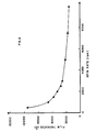
- the thickness of the cured films as determined by ellipsometry is given in Figure 2.
- the refractive index of the films was incidentally measured and ranged from 1.48 to 1.55.
- the surface resistivity was found to be about 10 12 ohm-centimeters and the bulk resistivity about 10 13 ohm-centimeters, on related but different samples.
- the dielectric constant was determined to be between 3.5 to 4.0 on different but related samples.
- the dielectric strength was in a range from 0.5 to 1.8 x 10 6 volts per centimeter.
- the cured films were effectively free from defects and pinholes when sufficient care was taken to keep particulates out of the solution. Subsequent layers could be spun on top of one another to yield multiple layers having an overall thickness as expected. Regardless of the number of layers, adhesion was found to be excellent as determined by ASTM D-3359, Method B. In this test, (i) the adhered film is cut into small squares; (2) scotch tape is firmly pressed on top of the cut squares; (3) the scotch tape is pulled from the film; and (4) the number of squares that are dislodged, counted.
- a water absorption test (at 100% relative humidity and 85 0 C) showed that the film on a silicon wafer substrate had absorbed less than 0.1% by weight over a six day period.
- Example 2A Example 1 was essentially repeated except that there was delayed addition of the phosphorus monomer rather than delayed addition of the boron monomer.
- the TGA decomposition temperature was found to be 570°C (rather than 575°C).
- the weight loss was 0.0% from 300°C to 400 0 C; and 1.7% from 400°C to 500 0 C.
- Example 2B Example 1 was essentially repeated except that there was delayed addition of the silicon monomer, rather than the boron monomer. In other words, the boron monomer was pre-reacted with the phosphorus monomer before addition of the silicon monomer. Also the silicon monomer was WACKER SILICONE INTERMEDIATE SY 430. [According to Wacker-Chemie GmbH's technical bulletin SME 10-165.8210 entitled Wacker Silicone Intermediate SY 430, published October 1982, it is a silanol functional pure phenyl silicone resin, in the form of flakes. It has a silicone content of 98% minimum by ASTM-D 1346 (1.5g/3h/135°C). It has a hydroxyl content of 5% minimum.
- Example 3A Example 1 was essentially repeated except that the boron monomer was omitted, and the phosphorus monomer was present at a level of 3% by weight. Dry powdered samples of the uncured resin had a decomposition temperature of about 560°C (rather than 575°C). Weight loss was little changed, at 0.2% from 300°C to 400°C; and 1.5% from 400°C to 500°C.
- Example 38 Example 3A was repeated except that phosphorus monomer was present at a concentration of 6.0%. The decomposition temperature fell to 555°C.
- Example 3C Example 3A was repeated at a phosphorus monomer concentration of 12%.
- the decomposition temperature was 540°C.
- Example 3D Example 3A was repeated except that the phosphorus monomer was present at a concentration of 25%.
- the decomposition temperature was much lower at about 460°C.
- This Example illustrates the effect of omitting the phosphorus monomer.
- Example 1 was essentially repeated except that the phosphorus monomer was omitted.
- the amount of triisopropylborate used was 7.3% by weight.
- the silicon monomer was WACKER SILICONE INTERMEDIATE SY 430.
- the weight loss was about 0.6% up to 400°C, and about 2% between 400 and 500°C.
- the decomposition temperature was about 5 40 o C .
- PPA phenylphosphonic acid
- TAB tri-n-butylborate
- TIPB triisopropylborate
- Example 5A Example 2A was essentially repeated except that 2.9% of PPA and 4.1% of TBB were used.
- the decomposition temperature was found to be 570°C.
- the weight loss was 1.2% from 300°C to 400°C; and 1.8% from 400°C to 500°C.
- Example 5B Example 2B was essentially repeated except that 1.5% of PPA and 4.5% of TBB were used.
- the decomposition temperature was about 565°C.
- the weight loss was 0.8% from 300°C to 400°C; and 2.4% from 400°C to 500°C.
- Example 5C Example 2A was essentially repeated except that 1.1% of PPA and 8.4% of TBB were used.
- the decomposition temperature was about 550°C.
- the silicon monomer was WACKER SILICONE INTERMEDIATE SY 430.
- the weight loss was 2.2% from 300°C to 400°C; and 1.8% from 400°C to 500°C.
- Example 6A Example 4 was essentially repeated except that 3.0% of phenylboron dihydroxide (PBDH) was used rather than 7.3% TIPB.
- PBDH phenylboron dihydroxide
- the decomposition temperature was only 550°C.
- the weight loss was 0.8% from 300°C to 400°C; and 3.2% from 400°C to 500°C.
- Example 6B Example 6A was essentially repeated except that 12% of PBDH was used rather than 3.0%.
- the decomposition temperature was about 540°C.
- the weight loss was about 1.7% from 300°C to 400°C; and 3.0% from 400°C to 500°C.
- C2 Various potential spin-coating compositions (C2) were prepared in a manner generally similar to the procedures of Example 1(i).
- Example 7A a mixture of cyclohexanol and xylene (in a 1/1 ratio by weight) was used.
- the film thickness obtainable in a spin-coating operation was greater than that under corresponding conditions in Example 1.
- Example 7B pure benzyl alcohol was used in place of xylene.
- the product could not be spun-coated to give a product with a measurable film thickness.
- Example 7C benzyl alcohol/xylene was used in a 1/1 ratio. Results were similar to Example 7B.
- Example 7D benzyl ether was used in place of xylene. Results were similar to Example 7B.
- Example 7E benzyl ether/xylene was used in a 1/1 ratio. Results were similar to Example 7B.
- This Comparative Example is not prior art. It illustrates the properties obtained when neither phosphorus nor boron is incorporated into the cured resin.
- a sample of WACKER SILICONE INTERMEDIATE SY 430 was dissolved in xylene such that the weight percent was 20% solids.
- a wafer was coated and processed with this solution as generally described in Example 1.
- the angular spin rate was about 5000 rpm and a thickness of about 3300 Angstroms was observed.
- the quality of this film was poor. It had small pinholes and was non-uniform.
- the above coated-wafer was then treated with the same amount of the solution in an attempt to increase the film thickness. No increase in the measured thickness of the film was observed by ellipsometry. The resulting total thickness was still only 3300 Angstroms.
- the decomposition temperature of the film was about 565°c.
Landscapes
- Chemical & Material Sciences (AREA)
- Organic Chemistry (AREA)
- Health & Medical Sciences (AREA)
- Chemical Kinetics & Catalysis (AREA)
- Medicinal Chemistry (AREA)
- Polymers & Plastics (AREA)
- Physics & Mathematics (AREA)
- Spectroscopy & Molecular Physics (AREA)
- Life Sciences & Earth Sciences (AREA)
- Engineering & Computer Science (AREA)
- Materials Engineering (AREA)
- Wood Science & Technology (AREA)
- Paints Or Removers (AREA)
- Silicon Polymers (AREA)
- Formation Of Insulating Films (AREA)
- Polymers With Sulfur, Phosphorus Or Metals In The Main Chain (AREA)
- Organic Insulating Materials (AREA)
- Internal Circuitry In Semiconductor Integrated Circuit Devices (AREA)
Applications Claiming Priority (2)
| Application Number | Priority Date | Filing Date | Title |
|---|---|---|---|
| US06/733,690 US4663414A (en) | 1985-05-14 | 1985-05-14 | Phospho-boro-silanol interlayer dielectric films and preparation |
| US733690 | 1985-05-14 |
Publications (2)
| Publication Number | Publication Date |
|---|---|
| EP0202108A2 true EP0202108A2 (fr) | 1986-11-20 |
| EP0202108A3 EP0202108A3 (fr) | 1988-06-15 |
Family
ID=24948726
Family Applications (1)
| Application Number | Title | Priority Date | Filing Date |
|---|---|---|---|
| EP86303627A Withdrawn EP0202108A3 (fr) | 1985-05-14 | 1986-05-13 | Couches intermédiaires à base de silanols contenant du phosphore et du bore dans la fabrication de films diélectriques |
Country Status (5)
| Country | Link |
|---|---|
| US (1) | US4663414A (fr) |
| EP (1) | EP0202108A3 (fr) |
| JP (1) | JPS61261370A (fr) |
| KR (1) | KR860009088A (fr) |
| IL (1) | IL78383A0 (fr) |
Cited By (3)
| Publication number | Priority date | Publication date | Assignee | Title |
|---|---|---|---|---|
| US6914114B2 (en) | 2000-07-17 | 2005-07-05 | Honeywell International Inc. | Absorbing compounds for spin-on-glass anti-reflective coatings for photolithography |
| WO2014105959A1 (fr) * | 2012-12-28 | 2014-07-03 | Dow Corning Corporation | Composition durcissable d'organopolysiloxane pour transducteurs et applications de cette composition durcissable de silicone pour des transducteurs |
| US9947858B2 (en) | 2012-12-28 | 2018-04-17 | Dow Corning Corporation | Curable organopolysiloxane composition for transducers and applications of such curable silicone composition for transducers |
Families Citing this family (16)
| Publication number | Priority date | Publication date | Assignee | Title |
|---|---|---|---|---|
| FR2591587A1 (fr) * | 1985-12-17 | 1987-06-19 | Saint Gobain Vitrage | Film organo-mineral depose sur un substrat en verre eventuellement revetu d'une ou plusieurs couches metalliques minces. |
| US4758620A (en) * | 1987-07-02 | 1988-07-19 | Akzo America Inc. | Blend of solvent and arylsiloxane interlayer dielectric materials |
| US4765866A (en) * | 1987-07-02 | 1988-08-23 | Akzo America Inc. | Energy ray curing of arylsiloxane/silicate compositions and subsequent etching thereof |
| US4801507A (en) * | 1987-07-02 | 1989-01-31 | Akzo American Inc. | Arylsiloxane/silicate compositions useful as interlayer dielectric films |
| US5089303A (en) * | 1989-04-24 | 1992-02-18 | Akzo America Inc. | Blend of solvent and photocurable arylsiloxane materials |
| US5527872A (en) * | 1990-09-14 | 1996-06-18 | At&T Global Information Solutions Company | Electronic device with a spin-on glass dielectric layer |
| EP1190277B1 (fr) * | 1999-06-10 | 2009-10-07 | AlliedSignal Inc. | Semiconducteur ayant un enduit antireflet spin-on-glass pour photolithographie |
| SE521977C2 (sv) * | 2002-06-20 | 2003-12-23 | Mobile Media Group Stockholm A | Metod och apparat för att formatera en webbtjänst |
| US8053159B2 (en) | 2003-11-18 | 2011-11-08 | Honeywell International Inc. | Antireflective coatings for via fill and photolithography applications and methods of preparation thereof |
| US8642246B2 (en) | 2007-02-26 | 2014-02-04 | Honeywell International Inc. | Compositions, coatings and films for tri-layer patterning applications and methods of preparation thereof |
| US8557877B2 (en) | 2009-06-10 | 2013-10-15 | Honeywell International Inc. | Anti-reflective coatings for optically transparent substrates |
| US8864898B2 (en) | 2011-05-31 | 2014-10-21 | Honeywell International Inc. | Coating formulations for optical elements |
| US9006101B2 (en) * | 2012-08-31 | 2015-04-14 | Taiwan Semiconductor Manufacturing Company, Ltd. | Interconnect structure and method |
| US9076719B2 (en) | 2013-08-21 | 2015-07-07 | The Regents Of The University Of California | Doping of a substrate via a dopant containing polymer film |
| JP6072129B2 (ja) | 2014-04-30 | 2017-02-01 | ザ リージェンツ オブ ザ ユニバーシティ オブ カリフォルニア | ドーパント含有ポリマー膜を用いた基体のドーピング |
| JP6803842B2 (ja) | 2015-04-13 | 2020-12-23 | ハネウェル・インターナショナル・インコーポレーテッドHoneywell International Inc. | オプトエレクトロニクス用途のためのポリシロキサン製剤及びコーティング |
Family Cites Families (6)
| Publication number | Priority date | Publication date | Assignee | Title |
|---|---|---|---|---|
| US3414463A (en) * | 1968-01-04 | 1968-12-03 | Owens Illinois Inc | Organopolysiloxane modified with an organophosphorus compound and use thereof |
| DE2040180B2 (de) * | 1970-01-22 | 1977-08-25 | Intel Corp, Mountain View, Calif. (V.St.A.) | Verfahren zur verhinderung von mechanischen bruechen einer duennen, die oberflaeche eines halbleiterkoerpers ueberdeckende isolierschichten ueberziehenden elektrisch leitenden schicht |
| US4218571A (en) * | 1975-12-08 | 1980-08-19 | Mobil Oil Corporation | Olefin hydrogenation over synthetic amorphous silica |
| JPS5760330A (en) * | 1980-09-27 | 1982-04-12 | Fujitsu Ltd | Resin composition |
| DE3213247A1 (de) * | 1981-04-13 | 1982-12-02 | Showa Electric Wire & Cable Co., Ltd., Kawasaki, Kanagawa | Polyborsiloxan-ueberzugsmasse und isolierter elektrischer leiter |
| JPS59199756A (ja) * | 1983-04-27 | 1984-11-12 | Toshiba Silicone Co Ltd | 導電性シリコ−ンゴム組成物 |
-
1985
- 1985-05-14 US US06/733,690 patent/US4663414A/en not_active Expired - Fee Related
-
1986
- 1986-03-28 KR KR1019860002316A patent/KR860009088A/ko not_active Ceased
- 1986-03-31 IL IL78383A patent/IL78383A0/xx unknown
- 1986-05-13 EP EP86303627A patent/EP0202108A3/fr not_active Withdrawn
- 1986-05-13 JP JP61107792A patent/JPS61261370A/ja active Pending
Cited By (4)
| Publication number | Priority date | Publication date | Assignee | Title |
|---|---|---|---|---|
| US6914114B2 (en) | 2000-07-17 | 2005-07-05 | Honeywell International Inc. | Absorbing compounds for spin-on-glass anti-reflective coatings for photolithography |
| WO2014105959A1 (fr) * | 2012-12-28 | 2014-07-03 | Dow Corning Corporation | Composition durcissable d'organopolysiloxane pour transducteurs et applications de cette composition durcissable de silicone pour des transducteurs |
| US9879126B2 (en) | 2012-12-28 | 2018-01-30 | Dow Corning Corporation | Curable organopolysiloxane composition for transducers and applications of such curable silicone composition for transducers |
| US9947858B2 (en) | 2012-12-28 | 2018-04-17 | Dow Corning Corporation | Curable organopolysiloxane composition for transducers and applications of such curable silicone composition for transducers |
Also Published As
| Publication number | Publication date |
|---|---|
| KR860009088A (ko) | 1986-12-20 |
| IL78383A0 (en) | 1986-07-31 |
| US4663414A (en) | 1987-05-05 |
| EP0202108A3 (fr) | 1988-06-15 |
| JPS61261370A (ja) | 1986-11-19 |
Similar Documents
| Publication | Publication Date | Title |
|---|---|---|
| US4663414A (en) | Phospho-boro-silanol interlayer dielectric films and preparation | |
| EP0610899B1 (fr) | Procédé de formation d'une couche en oxyde de silicium | |
| EP1245642B1 (fr) | Résine de polysiloxane et méthode de la production d' une couche intermédiaire pour plaquettes | |
| EP0112168B1 (fr) | Compositions de revêtement à base de polysiloxanes et leur préparation | |
| JP4662718B2 (ja) | 集積回路用途用の低金属多孔質シリカ誘電体 | |
| CN100383147C (zh) | 多官能环状硅氧烷化合物和由该化合物制备的硅氧烷基聚合物和用该聚合物制备介电薄膜的方法 | |
| Huang et al. | Structure-property behavior of new hybrid materials incorporating oligomeric poly (tetramethylene oxide) with inorganic silicates by a sol-gel process: 3. Effect of oligomeric molecular weight | |
| US6623711B2 (en) | Siloxane-based resin and method for forming insulating film between interconnect layers in semiconductor devices by using the same | |
| KR20020042727A (ko) | 유기실세스퀴옥산 전구물질을 사용한 막 증착 | |
| US5045592A (en) | Metastable silane hydrolyzates | |
| JP4549781B2 (ja) | 新規のシロキサン樹脂及びこれを用いた半導体層間絶縁膜 | |
| JP4549832B2 (ja) | 多反応性線形シロキサン化合物、当該化合物から製造されるシロキサン系重合体及び当該重合体を用いた絶縁膜の製造方法 | |
| EP1230311A1 (fr) | Depot de films de silsesquioxane fluores | |
| CN100393730C (zh) | 多官能环状硅酸盐(或酯)化合物,由该化合物制得的基于硅氧烷的聚合物和使用该聚合物制备绝缘膜的方法 | |
| EP1493773A1 (fr) | Résines à base de siloxanes et couche isolante intermediaire pour semiconducteur faits de celle-ci | |
| EP1484354B1 (fr) | Résine à base de siloxane et couche intermédiaire isolante pour dispositifs semiconducteurs | |
| EP0218117A2 (fr) | Polymères polycyclosilazanes et leur emploi comme film diélectrique dans la fabrication de circuits intégrés | |
| US7744946B2 (en) | Organic siloxane resins and insulating film using the same | |
| WO2008082128A1 (fr) | Copolymeres de silsesquioxane a base de norbornene, derive de silane a base de norbornene utilise dans la preparation de ces copolymeres et procede de preparation d'un film isolant a faible constante dielectrique contenant ces copolymeres | |
| US20020136910A1 (en) | Deposition of organosilsesquioxane films | |
| EP1498443A1 (fr) | Résine à base de siloxane contenant du gemanium et couche intermédiaire isolante pour semi-conducteur la contenant | |
| US7338689B2 (en) | Composition for forming low dielectric thin film including siloxane monomer or siloxane polymer having only one type of stereoisomer and method of producing low dielectric thin film using same | |
| US4801507A (en) | Arylsiloxane/silicate compositions useful as interlayer dielectric films | |
| US6908977B2 (en) | Siloxane-based resin and method of forming an insulating film between interconnect layers of a semiconductor device using the same | |
| KR100585940B1 (ko) | 폴리카프락톤 유도체를 포함하는 나노기공성 조성물 및그를 이용한 반도체용 층간 절연막의 형성방법 |
Legal Events
| Date | Code | Title | Description |
|---|---|---|---|
| PUAI | Public reference made under article 153(3) epc to a published international application that has entered the european phase |
Free format text: ORIGINAL CODE: 0009012 |
|
| AK | Designated contracting states |
Kind code of ref document: A2 Designated state(s): BE CH DE FR GB IT LI SE |
|
| PUAL | Search report despatched |
Free format text: ORIGINAL CODE: 0009013 |
|
| AK | Designated contracting states |
Kind code of ref document: A3 Designated state(s): BE CH DE FR GB IT LI SE |
|
| 17P | Request for examination filed |
Effective date: 19881118 |
|
| RAP1 | Party data changed (applicant data changed or rights of an application transferred) |
Owner name: AKZO N.V. |
|
| 17Q | First examination report despatched |
Effective date: 19910212 |
|
| RAP1 | Party data changed (applicant data changed or rights of an application transferred) |
Owner name: NATIONAL STARCH AND CHEMICAL INVESTMENT HOLDING CO |
|
| STAA | Information on the status of an ep patent application or granted ep patent |
Free format text: STATUS: THE APPLICATION IS DEEMED TO BE WITHDRAWN |
|
| 18D | Application deemed to be withdrawn |
Effective date: 19921002 |
|
| RIN1 | Information on inventor provided before grant (corrected) |
Inventor name: ESTES, WILLIAM EDWARD Inventor name: MARSH, WAYNE EDWARD |