EP0204034A2 - Réseau logique configurable - Google Patents
Réseau logique configurable Download PDFInfo
- Publication number
- EP0204034A2 EP0204034A2 EP85200590A EP85200590A EP0204034A2 EP 0204034 A2 EP0204034 A2 EP 0204034A2 EP 85200590 A EP85200590 A EP 85200590A EP 85200590 A EP85200590 A EP 85200590A EP 0204034 A2 EP0204034 A2 EP 0204034A2
- Authority
- EP
- European Patent Office
- Prior art keywords
- leads
- logic
- lead
- inverter
- configurable logic
- Prior art date
- Legal status (The legal status is an assumption and is not a legal conclusion. Google has not performed a legal analysis and makes no representation as to the accuracy of the status listed.)
- Granted
Links
Images








Classifications
-
- G—PHYSICS
- G11—INFORMATION STORAGE
- G11C—STATIC STORES
- G11C19/00—Digital stores in which the information is moved stepwise, e.g. shift registers
- G11C19/28—Digital stores in which the information is moved stepwise, e.g. shift registers using semiconductor elements
Definitions
- This invention relates to programmable logic arrays and in particular, to a method for providing on-chip programming of each of a plurality of logic elements formed on a chip of semiconductor material to configure each logic element to carry out certain desired functions.
- Gate arrays are well known in the prior art. Typically a gate array is produced by interconnecting a plurality of active devices in a base array in any one of a number of ways to achieve a desired logic function. As gate arrays become more complex, the simulation of the logic to be achieved from a given interconnection of the active devices in the base array becomes more difficult and is typically carried out using a computer program. The layout of the actual interconnections for the active devices in the base array to yield a finished gate array is then derived using a computer aided design program of a type well known in the art. The process of designing such a structure is complex and reasonably expensive requiring the use of logic simulation and verification programs and semiconductor device layout programs. Accordingly, a need exists for an alternative approach which significantly simplifies the obtaining of a given logic function from a base array.
- I provide a structure which I denote as a configurable logic array which allows changing the configuration of the finished integrated circuit from time-to-time (even when the integrated circuit is installed in a system) to provide any one of a plurality of logical functions from the same integrated circuit.
- a new type of integrated circuit is achieved which is capable of being configured to provide any one of a plurality of logic functions depending upon the tasks which the system of which it is a part is called upon to perform.
- configurable logical element I mean a combination of devices which are capable of being electrically interconnected by switches operated in response to control bits to form any one of a plurality of logical functions.
- a configurable logic array of my invention is comprised of a multiplicity of configurable logic elements each of which can include all the circuit elements necessary to provide one or more of the functions provided by an AND gate, flip flop, inverter, NOR gate, exclusive OR gate, and combinations of these functions to form more complex functions.
- the particular function to be carried out by a configurable logic element is determined by control signalz applied to the configurable logic element from control logic.
- the configurable logic element of one embodiment of my invention can function as an AND gate, an OR gate, a NOR gate, a NAND gate or an exclusive OR gate or any one of a number of other logic elements without any change in physical structure.
- structure is provided to allow any one of a plurality of functions to be selected from each configurable logic element. This is done by providing control logic to store and generate control signals which control the configuration of each configurable logic element.
- control signals are stored and transmitted by control logic formed integrally with and as part of the integrated circuit chip containing the configurable logic element.
- control information can be stored and/or generated outside this integrated circuit and transmitted through pins to the configurable logic element.
- a given set of control signals is transmitted to one configurable logic element to control the configuration of that configurable logic element.
- the control logic is thus arranged to provide any one set of a plurality of sets of control bits to each configurable logic element on the chip.
- the actual set of control bits provided to each configurable logic element on the integrated circuit chip depends on the function to be carried out by the integrated circuit chip or by each configurable logic element on the chip.
- the configuration of each logic element on the chip is determined by the intended function of the total chip and by the intended formation of that configurable logic element as part of the chip.
- the resulting structure is known as a "Configurable Logic Array" or "CLA” and each logic element in the array is known as a “Configurable Logic Element” or "CLE”.
- each integrated circuit chip has in addition to and associated with the control logic certain on-chip data routing circuitry.
- the on-chip data routing is achieved by using a memory to store the particular data used to configure the configurable logic elements and by then transferring the data from the memory to a novel combination of a dynamic shift register and static latch element within or associated with each configurable logic element on the chip.
- the particular structure of this invention is versatile in that it can be implemented particularly easily using P channel, N channel, or CMOS technologies in the embodiment shown. Of course, structure incorporating the principles of this invention can, if desired, be implemented using any other appropriate semiconductor technology.
- the novel dynamic shift register-static latch element of this invention is particularly useful in that the structural "overhead" (i.e., access circuitry and routing circuitry) is kept to a minimum relative to the useful logic functions on the total chip. Of particular importance, no addressing, data selection, or decoding in each configurable logic element is necessary when this novel combination of a dynamic shift register and static latch element is used to implement the configurable logic array of my invention.
- Figure 1 illustrates certain logic functions capable of being integrated into a configurable logic element.
- the 28 functions shown in Figure 1 are merely illustrative and other elements not shown can, if desired, be included in a configurable logic element.
- the following elements are shown:
- Figure 2 illustrates the internal logic structure of one possible logic element which is capable of implementing all useful functions of the two variables A and B, with the functions being selected by configuration control signals C0, CO , Cl, C1 ... through C5, as shown in Figure 1.
- configuration control signals C0, CO , Cl, C1 ... through C5 as shown in Figure 1.
- the input leads labeled A and B are shunted past inverters 21 and 22, respectively, by high level signals on the Cl and CO configuration control leads.
- Leads C1 and CO are connected to well-known pass transistors 29c and 29d. (Throughout this specification a pass transistor will be represented by the symbol shown within the circles 29c and 29d).
- Low level signals are applied to the configuration control leads CO , C1 , C4.
- control signals, C2, C2 , C3 and ⁇ 3 are "don't cares". That is, these signals can be high or low without affecting the output signal.
- a high level signal on C5 ig applied to enable AND gate 25.
- the high level signal from AND gate 25 is passed through NOR gate 26.
- this signal proceeds as a low level signal to turn off MOS transistor 29a (the source of which is grounded and the drain of which is connected to the output lead 28) and to turn on through NOR gate 27 N channel transistor 29b (the drain of which is connected to a power supply and the source of which is connected to both the output lead 28 and the drain of N channel transistor 29a).
- MOS transistor 29a the source of which is grounded and the drain of which is connected to the output lead 28
- N channel transistor 29b the drain of which is connected to a power supply and the source of which is connected to both the output lead 28 and the drain of N channel transistor 29a.
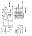
- Figure 3A illustrates a 16 bit RAM capable of to producing an output signal in response to any one of sixteen possible combinations of input signals.
- input signals A and B control the X decoder to select any one of the four columns in the 16 bit RAM.
- Input signals C and D control the Y decoder to select any one of the four rows in the 16 bit RAM.
- the 16 bit RAM produces an output signal representative of the bit at the intersection of the selected row and column. There are 16 such intersections and thus sixteen such bits.
- NOR gate is to be simulated by the 16 bits in the RAM, the Karnough map for the RAM would be as shown in Figure 3C.
- Figure 3B shows another structure for yielding any one of sixteen select bits.
- Each of registers 0-15 in the vertical column to the left labelled “16 Select Bits”, contains a selected signal, either a binary 1 or 0.
- a particular bit stored in a particular one of the sixteen locations in the 16 Select Bits register is transmitted to the output lead.
- the signal A, B, C, D is applied to the leads so labeled.
- the signal A, B, C, and ⁇ is applied to the appropriate columns.
- any one of 216 logic functions can be implemented using this structure.
- Figures 4A illustrates an embodiment of a of a configurable logic array of this invention containing nine configurable logical elements. As shown in Figure 4A, nine logical elements are placed on an integrated circuit chip together with interconnects and variable switches for connecting various leads to other leads.
- Each of logic elements 40-1 through 40-9 represents a collection of circuitry such as that shown in Figure 2 or some similar structure capable of being configured as described above in Figure 2 to perform any one of a number of logic functions. To program the circuitry, selected signals are applied to input leads identified as configuration control input leads thereby to generate a desired logical function in each of the logic elements.
- no specific lead has been identified as an input lead for the configuration control signals. However, any particular I/O pad can be selected for this purpose.
- the configuration control bids can be input into the configurable logic array either in series or in parallel depending upon design considerations.
- another I/O pad will be used on input clock signals to clock the logic elements both for the shifting in of the configuration control signals to each configurable logic element and for controlling the operation of each logic element during the functioning of the integrated circuit chip in its intended manner.
- the combination of logic elements 40-1 through 40-9 yields the desired logical output for the Configurable Logic Array.
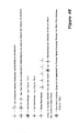
- Figure 4B illustrates the meaning of the interconnect symbols used in Figure 4A.
- FIG. 5 illustrates a novel shift register of use in this invention.
- the shift register of Figure 5 is illustrated showing two basic storage cells. Each storage cell is capable of storing one bit of information.
- an actual shift register will contain as many storage cells as required to configure the logic element of which the shift register is a part, to its desired configuration.
- an input signal is applied to input lead 58.
- This input signal (shown in Figure 6D) contains the pulses to be stored in the shift register as configuration control bits to configure the configurable logic element to perform a desired logic function or to configure an interconnection between leads in a manner to be described shortly.
- the sequence of pulses applied to input lead 58 represents those pulses which when stored in the storage cells of the shift register will activate the configuration control bits in the proper manner to achieve the desired functional and/or interconnection result.
- the pulses C0, Cl, C2, C3, C4, and C5 would be represented by 1,1,X,X, 0,1.
- the sequence of pulses applied to input lead 58 is synchronized with clocking pulses ⁇ 1 and ⁇ 2 applied to leads 57 and 59 respectively.
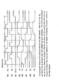
- clocking pulse ⁇ 1 goes high (Fig. 6A)
- clocking pulse 4*2 is low (Fig. 6B)
- the hold signal (Fig. 6C) is low during shifting thereby facilitating the passage of data through sequentially connected cells 5-1, 5-2 et al. of the shift register.
- the input signal on lead 58 is low during approximately the first half cycle of the clocking period tl.
- the output signal Q1 of inverter 51-1 goes to a high level in response to the low level input signal and ⁇ 1 high to enable PASS transistor 53-1.
- the previous low level signal on Ql has driven the output signal Q2 of inverter 51-2 to a high level when Ql was at a high level to enable PASS transistor 53-2 and the change in ⁇ 2 from a low level to a high level in the second half of period t2 to enable PASS transistor 55-2 drives the output signal Q2 from inverter 52-2 to a low level.
- the input signal on lead 58 (Fig. 6D) is transmitted through each of the cells 5-1, 5-2, 5-3 et al. in the shift register.
- the hold signal ( Figure 6C) is enabled (i.e., driven to a high level) thereby to connect the feedback leads 50-1, 50-2, and 50-3 et al. from the output leads of inverters 52 to the input leads of inverters 51 so as to hold the information then in each cell indefinitely.
- the signal stored in a given cell 5 is connected to a configuration control or to an interconnect pass device.
- the Q 1 , Q 1' Q 1 , Q 2' etc., of the shift register are directly connected to the (configuration) control inputs of a logic unit or the pass devices of the configurable interconnect.
- the shift register operates in its dynamic phase by storing the information being shifted as charge on the gates of the transistors (not shown in Figure 5 but well-known) comprising inventers 51-1, 52-1, 51-2, 52-2 et al. of the shift register. These inverters are of well-known design and will not be described in detail.
- the use of dynamic shift register is an important feature of the invention because a dynamic shift register uses six transistors and thus takes up very little area. Uniquely, the dynamic shift register is converted to a static latch by adding only one transistor. Thus the novel dynamic shift register-static latch can be easily fabricated as part of a configurable logic element without adding significant complexity to the circuit or consuming significant semiconductor area. Because of the "hold" signal, the dynamic shift register can be driven at a very low frequency because placing the shift register on hold automatically refreshes the data. Thus a separate refresh circuit is not needed.
- the novel, dynamic shift register static latch circuit is unique in that it does not need refreshing once it has been latched into a hold position. This is accomplished by use of the feedback circuit comprising lead 50-1 and pass transistor 54-1 in cell 5-1, for example.
- Figure 7A shows an additional configurable logic array containing a plurality of configurable logic elements.
- configurable logic elements 70-1, 70-2, 70-4 and 70-5 are shown in their entirety while configurable logic elements 70-3, 70-6 and 70-7 through 70-9 are shown partially.
- the complete interconnections of these last five logical elements are not shown.
- the structure shown in Figure 7A is merely illustrative of the types of configurations and connections which can be implemented using the configurable logic array of this invention and does not depict an actual circuit configured to carry out an intended function.
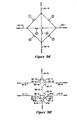
- Figure 9A is the schematic of a circuit for making a number of different interconnections between two cross-over leads, horizontal lead 90-1 and vertical lead 90-2.
- pass transistor 2 when activated into the conducting state, connects lead 90-3 to lead 90-1.
- Pass transistor 1 when conducting, connects lead 90-3 to lead 90-4.
- Pass transistor 4 when conducting, connects lead 90-4 to lead 90-2 and pass transistor 3, when conducting, connects lead 90-1 to lead 90-2.
- pass transistor 6 is activated.
- pass transistor 5 is activated.
- a simplified notation system as shown in Figures 9B to 9E has been adopted.
- FIG 9B a plurality of pass transistors 92-1 through 92-13 are shown.
- the convention adopted in Figure 9B is to have a given pass transistor represented by a single short line.
- the line labelled 92-1 represents a pass transistor.
- Pass transitor 92-1 is drawn so that its two ends point to the ends of the leads 91-5 and 91-6 being interconnected by pass transistor 92-1.
- the right end 93a of pass transistor 92-1 is aimed to the end 94a of lead 91-5.
- the left end 93b of pass transistor 92-1 is aimed to the end 94b of lead 91-6.
- the other ends of the transistors are not labelled.
- pass transistor 92-7 interconnects horizontal lead 91-4 with horizontal lead 91-1.
- Pass transistor 92-13 interconnects horizontal lead 91-4 with horizontal lead 91-2.
- Pass transistor 92-12 interconnects lead 91-3 with lead 91-5. Similar connections can be made between the other pass transistors and the other leads.
- lead 91-3 can be connected by turning on pass transistor 92-10 to lead 91-2.
- lead 91-3 can be connected to lead 91-4 by turning on pass transistor 92-13.
- lead 91-3 could be connected to lead 91-4 by turning on pass transistor 92-11.
- lead 91-6 could be connected to the three leads 91-2, 91-3, 91-4 by turning on pass transistor 92-8. The number of interconnections which can be made using this structure is limited only by the imagination of the designer.
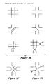
- FIG 9D another possible interconnection topology is illustrated.
- leads 1 to 8 are shown coming together at a complicated intersection.
- Leads 1 and 8 are parallel horizontal to the left
- leads 4 and 5 are parallel horizontal to the right
- leads 2 and 3 are parallel vertical up
- leads 6 and 7 are parallel vertical down.
- lead 6 the end 6a of lead 6 can be connected sensibly to the ends "a" of leads 1, 2, 3 , 4, 5 and 8. It is not sensible to connect lead 6 to lead 7 because theoretically the two leads are going in one direction only one lead is required to carry the necessary information in that direction. Since lead 6 has six possible connections and there are eight leads, a total of forty-eight possible connections are offered by the structure of Figure 9D.
- Figure 9E illustrates types of interconnections possible using the method of this invention.
- the leads interconnected are illustrated by showing continuous lines or broken lines depending on whether a given lead is connected to another lead or left unconnected. These interconnections are self-explanatory.
- Figure 9F illustrates the connections that would be possible if the four pass transistors omitted from Figure 9D were in fact included.
- the dashed lines show the interconnections possible by these omitted transistors.
- Figure 9D shows only twenty pass transistors whereas twenty-four pass transistors are necessary to make all possible nonsimple connections.
- Figure 9G illustrates, however, the way in which it is possible to interconnect leads 4 and 7 without the four transistor connections shown in Figure 9F being present.
- lead 4 is connected directly to lead 8 by means of transistor 4-8 while lead 8 is connected to lead 7 by pass transistor 8-7.
- Figure 9C illustrates the configuration of Figure 9D with the full twenty-four interconnection transistors shown rather than merely the twenty shown in Figure 9D.
- pass transistors 1-6, 7-4, 2-5 and 8-3 have been added to the transistors shown in Figure 9D.
- the other pass transistors shown in Figure 9D have not been numbered in Figure 9C except for pass transistor 6-8.
- Figures 7B-1 through 7B-7 are identical to the symbology just explained in conjunction with Figures 9A through 9G.
- Figure 7B-2 illustrates a solid block involving a twenty pass transistor interchange. This particular twenty transistor interchange is shown in more detail in Figure 7B-7 and corresponds precisely to the interchange explained above in conjunction with Figure 9D.
- Figure 7B-1 illustrates three transistors capable of making a T connection or a cross- connection but not a full interconnection.
- full interconnection is meant the ability to connect each of the leads (in Figure 7B-1, four leads) coming into a node to a given node or to each of the other leads coming into the node in any combination.
- Figure 7B-2 shows a one transistor interconnection to connect a row with a column.
- Figure 7B-3 shows a six transistor full cross interconnection wherein any one of four leads coming into a node can be connected to any one of the other three leads.
- Figure 7B-4 shows six leads coming into an intersection wherein ten pass transistors are used to interconnect any one of the six input leads to any one of the five other leads input to the node.
- Figure 7B-5 illustrates a four-lead node where two horizontal continuous leads are interconnected with two separate vertical leads using five pass transistors.
- Figure 7B-6 illustrates a three-transistor interconnection wherein any one of three leads coming into a node can be interconnected with any one of the other two leads.
- Figure 7B-7 illustrates the twenty-transistor interchange for interconnecting any one of eight input leads to any one of the other eight input leads except that lead parallel and adjacent to the lead being interconnected as illustrated in Figure 9D and except for the four interconnections shown in Figure 9F (which also cannot be directly made using the structure of Figure 7B-7).
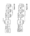
- FIGs 8A and 8B illustrate two possible systems capable of using the configurable logic arrays of this invention.
- a microprocessor microcontroller produces address signals, control signals and data signals which are transmitted to a master configurable logic array. Also shown as N slave CLAs.
- the control bits to control each of the configurable logic elements in each slave configurable logic array are transmitted on the data leads from the microcontroller to the master configurable logic array. From the master configurable logic array, this data is transmitted in series to each one of N configurable logic arrays where N is a selected integer.
- the control bits for controlling the configuration of each configurable logic element in each of the configurable logic arrays are transmitted in series through slave configurable logic array 1, slave configurable logic array 2 through to the Nth configurable array.
- the data is stored in serial shift registers as described above in conjunction with Figure 5.
- the hold signal shown in Figure 6C is raised to a high level thereby locking each data bit into the proper location in the corresponding shift register and thus configuring each configurable logic element in each configurable logic array.
- the data clock signals are applied on a separate lead to each configurable logic array as shown to clock in the control data.
- the address arrow pointing to CLA (master) in Figure 8A merely indicates that the microprocessor has the ability to select a particular master configurable logic array for receipt of data from the microprocessor.
- the master configurable logic array is capable going into the nonvolatile memory with addresses to select particular data to be retrieved from the memory to be used to configure each of the salve configurable logic arrays.
- the microprocessor produces address signals which will go to off chip memory or to other circuitry (not shown).
- Figure 8B the structure is similar to that shown in Figure 8A except that a nonvolatile memory such as a R O M, EPROM or E PROM is used as the source for the configuration control bits to be transmitted into each of the configurable logic arrays.
- a nonvolatile memory such as a R O M, EPROM or E PROM is used as the source for the configuration control bits to be transmitted into each of the configurable logic arrays.
- the structure of Figure 8B is unique in that when power is turned on or when a reset signal is applied to the master CLA, the master CLA initiates the transfer of the information for controlling the transfer of the information.for controlling or configuring the Configurable Logic Array from the non-volatile memory to the master CLS and to the slave CLAs 1to N. In this sense, the structure of Figure 8B is self-configuring in response to power on or a reset signal.
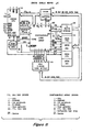
- Configurable Logic Array 110 performs the chip decode functions, the latching functions and the various special logic that is necessary to implement a single board microcomputer.
- the CLA has an output lead ("DONE") which is low from the time the power is turned on until the single board microcomputer is fully functional.
- the Configurable Logic Array 110 forces the Z8000 CPU 111 into the reset state. Reset forces the outputs of the CPU to be tri-stated (i.e., to go to high impedance level) which makes it possible for the Configurable Logic Array to use the control lines from the CPU 111 while it is being configured.
- the Configurable Logic Array 110 through a set of address lines (LA 1 - LA 12 ) addresses the EPROMS which are also used for the bootstrap of the microprocessor. In addition, the EPROMS have available in them configuration information for the CLA 110.
- the CLA 110 has signals which, during the self-loading time, are fixed high, fixed low so that particular bi-directional buffers 112 can be set in the correct direction for loading data from the EPROMS 113 to the Configurable Logic Array 110.
- Configurable Logic Array 110 then sequentially addresses locations in the EPROMS 113 which are read into the Configurable Logic Array 110 to configure the CLA 110.
- array 110 When array 110 is totally configured it then takes on its new functions and unlatches the done output which releases the reset line to the CPU 111.
- CPU 111 is then in control of the entire system.
- the decode used herein decodes the addresses from the CPU to create chip enables and chip selects for the various RAMS and EPROMS in the system and for the I/O devices as well.
- FIG. 10A shows the bi-directional buffer as comprising an inverter 101 connected into a second CMOS inverter comprising p-channel transistor 103 and n-channel transistor 104, the output lead of which is gated by pass transistor 108.
- inverter 102 feeds an input signal onto the gates of p-channel pass transistor 105 connected in series with n-channel transistor 106.
- the output at the node between the p- and n-channel transistors is controlled by pass transistor 107.
- the pass transistors 107 and 108 are activated by the Q, Q signals from the storage element which can comprise a standard flip-flop.
- the buffer passes a signal in one direction or the other on leads 109a or 109b, depending upon whether or not pass transistor 107 or pass transistor 108 is turned on.
- Figure 10B illustrates schematically the circuit of Figure 10A.
- the series connected p-channel and n-channel transistors 103 and 104 have been represented by inverter 103' and series connected p-channel pass transistor 105 and n-channel pass transistor 106 have been represented by inverter 105'.
- inverter 105' series connected p-channel pass transistor 105 and n-channel pass transistor 106
- directional amplifiers (shown by an X in a box) are used to amplify signals which have been attenuated by a number of pass transistors. This speeds up considerably the operation of the circuit. The delay of a signal increases approximately in proportion to the square of the number of pass transistors through which a signal must pass. The amplifer brings the signal voltage back to its normal level.
- a configurable logic element in a Configurable Logic Array is capable of being reconfigured even after the Configurable Logic Array has been installed in a circuit. Indeed, this is one of the key advantages of the Configurable Logic Array of this invention.
- a configurable Logic Array can be reconfigured to provide a new logical function as part of its normal operation in the system of which it is a part.
- I/O pads can be used as either input or output pads and can connect to any internal signal using pass transistors.
Landscapes
- Logic Circuits (AREA)
Priority Applications (2)
| Application Number | Priority Date | Filing Date | Title |
|---|---|---|---|
| EP85200590A EP0204034B1 (fr) | 1985-04-17 | 1985-04-17 | Réseau logique configurable |
| DE19853587944 DE3587944T2 (de) | 1985-04-17 | 1985-04-17 | Konfigurierbare logische Matrix. |
Applications Claiming Priority (1)
| Application Number | Priority Date | Filing Date | Title |
|---|---|---|---|
| EP85200590A EP0204034B1 (fr) | 1985-04-17 | 1985-04-17 | Réseau logique configurable |
Publications (3)
| Publication Number | Publication Date |
|---|---|
| EP0204034A2 true EP0204034A2 (fr) | 1986-12-10 |
| EP0204034A3 EP0204034A3 (en) | 1988-02-10 |
| EP0204034B1 EP0204034B1 (fr) | 1994-11-09 |
Family
ID=8194010
Family Applications (1)
| Application Number | Title | Priority Date | Filing Date |
|---|---|---|---|
| EP85200590A Expired - Lifetime EP0204034B1 (fr) | 1985-04-17 | 1985-04-17 | Réseau logique configurable |
Country Status (2)
| Country | Link |
|---|---|
| EP (1) | EP0204034B1 (fr) |
| DE (1) | DE3587944T2 (fr) |
Cited By (12)
| Publication number | Priority date | Publication date | Assignee | Title |
|---|---|---|---|---|
| WO1988003727A1 (fr) * | 1986-11-07 | 1988-05-19 | Concurrent Logic, Inc. | Cellule logique programmable et reseau |
| US4845633A (en) * | 1985-12-02 | 1989-07-04 | Apple Computer Inc. | System for programming graphically a programmable, asynchronous logic cell and array |
| GB2180382B (en) * | 1985-09-11 | 1989-11-22 | Pilkington Micro Electronics | Semi-conductor integrated circuits/systems |
| US5003200A (en) * | 1988-09-20 | 1991-03-26 | Kawasaki Steel Corporation | Programmable logic device having programmable wiring for connecting adjacent programmable logic elements through a single switch station |
| US5019736A (en) * | 1986-11-07 | 1991-05-28 | Concurrent Logic, Inc. | Programmable logic cell and array |
| US5089973A (en) * | 1986-11-07 | 1992-02-18 | Apple Computer Inc. | Programmable logic cell and array |
| US5144166A (en) * | 1990-11-02 | 1992-09-01 | Concurrent Logic, Inc. | Programmable logic cell and array |
| US5155389A (en) * | 1986-11-07 | 1992-10-13 | Concurrent Logic, Inc. | Programmable logic cell and array |
| US5371390A (en) * | 1990-10-15 | 1994-12-06 | Aptix Corporation | Interconnect substrate with circuits for field-programmability and testing of multichip modules and hybrid circuits |
| US5377124A (en) * | 1989-09-20 | 1994-12-27 | Aptix Corporation | Field programmable printed circuit board |
| US5400262A (en) * | 1989-09-20 | 1995-03-21 | Aptix Corporation | Universal interconnect matrix array |
| US7317332B2 (en) | 1999-03-04 | 2008-01-08 | Altera Corporation | Interconnection and input/output resources for programmable logic integrated circuit devices |
Families Citing this family (1)
| Publication number | Priority date | Publication date | Assignee | Title |
|---|---|---|---|---|
| DE102013003112B4 (de) | 2013-02-25 | 2017-06-14 | Umicore Ag & Co. Kg | SCR-Katalysator mit verbessertem NOx-Umsatz |
Family Cites Families (8)
| Publication number | Priority date | Publication date | Assignee | Title |
|---|---|---|---|---|
| GB1113111A (en) * | 1964-05-29 | 1968-05-08 | Nat Res Dev | Digital storage devices |
| US3439185A (en) * | 1966-01-11 | 1969-04-15 | Rca Corp | Logic circuits employing field-effect transistors |
| US3576984A (en) * | 1968-08-09 | 1971-05-04 | Bunker Ramo | Multifunction logic network |
| US3564514A (en) * | 1969-05-23 | 1971-02-16 | Honeywell Inc | Programmable logic apparatus |
| US3781570A (en) * | 1971-11-22 | 1973-12-25 | Rca Corp | Storage circuit using multiple condition storage elements |
| US3990045A (en) * | 1974-06-24 | 1976-11-02 | International Business Machines Corporation | Array logic fabrication for use in pattern recognition equipments and the like |
| US4566064A (en) * | 1982-05-10 | 1986-01-21 | American Microsystems, Inc. | Combinational logic structure using PASS transistors |
| US4642487A (en) * | 1984-09-26 | 1987-02-10 | Xilinx, Inc. | Special interconnect for configurable logic array |
-
1985
- 1985-04-17 EP EP85200590A patent/EP0204034B1/fr not_active Expired - Lifetime
- 1985-04-17 DE DE19853587944 patent/DE3587944T2/de not_active Expired - Lifetime
Cited By (21)
| Publication number | Priority date | Publication date | Assignee | Title |
|---|---|---|---|---|
| GB2180382B (en) * | 1985-09-11 | 1989-11-22 | Pilkington Micro Electronics | Semi-conductor integrated circuits/systems |
| US4935734A (en) * | 1985-09-11 | 1990-06-19 | Pilkington Micro-Electronics Limited | Semi-conductor integrated circuits/systems |
| US4845633A (en) * | 1985-12-02 | 1989-07-04 | Apple Computer Inc. | System for programming graphically a programmable, asynchronous logic cell and array |
| US4918440A (en) * | 1986-11-07 | 1990-04-17 | Furtek Frederick C | Programmable logic cell and array |
| US5019736A (en) * | 1986-11-07 | 1991-05-28 | Concurrent Logic, Inc. | Programmable logic cell and array |
| US5089973A (en) * | 1986-11-07 | 1992-02-18 | Apple Computer Inc. | Programmable logic cell and array |
| US5155389A (en) * | 1986-11-07 | 1992-10-13 | Concurrent Logic, Inc. | Programmable logic cell and array |
| WO1988003727A1 (fr) * | 1986-11-07 | 1988-05-19 | Concurrent Logic, Inc. | Cellule logique programmable et reseau |
| US5003200A (en) * | 1988-09-20 | 1991-03-26 | Kawasaki Steel Corporation | Programmable logic device having programmable wiring for connecting adjacent programmable logic elements through a single switch station |
| US5400262A (en) * | 1989-09-20 | 1995-03-21 | Aptix Corporation | Universal interconnect matrix array |
| US5544069A (en) * | 1989-09-20 | 1996-08-06 | Aptix Corporation | Structure having different levels of programmable integrated circuits interconnected through bus lines for interconnecting electronic components |
| US5377124A (en) * | 1989-09-20 | 1994-12-27 | Aptix Corporation | Field programmable printed circuit board |
| US5371390A (en) * | 1990-10-15 | 1994-12-06 | Aptix Corporation | Interconnect substrate with circuits for field-programmability and testing of multichip modules and hybrid circuits |
| US5504354A (en) * | 1990-10-15 | 1996-04-02 | Aptix Corporation | Interconnect substrate with circuits for field-programmability and testing of multichip modules and hybrid circuits |
| US5654564A (en) * | 1990-10-15 | 1997-08-05 | Aptix Corporation | Interconnect structure with programmable IC for interconnecting electronic components, including circuitry for controlling programmable IC |
| US5973340A (en) * | 1990-10-15 | 1999-10-26 | Aptix Corporation | Interconnect substrate with circuits for field-programmability and testing of multichip modules and hybrid circuits |
| US6160276A (en) * | 1990-10-15 | 2000-12-12 | Aptix Corporation | Double-sided programmable interconnect structure |
| US5144166A (en) * | 1990-11-02 | 1992-09-01 | Concurrent Logic, Inc. | Programmable logic cell and array |
| US7317332B2 (en) | 1999-03-04 | 2008-01-08 | Altera Corporation | Interconnection and input/output resources for programmable logic integrated circuit devices |
| US7492188B2 (en) | 1999-03-04 | 2009-02-17 | Altera Corporation | Interconnection and input/output resources for programmable logic integrated circuit devices |
| US7839167B2 (en) | 1999-03-04 | 2010-11-23 | Altera Corporation | Interconnection and input/output resources for programmable logic integrated circuit devices |
Also Published As
| Publication number | Publication date |
|---|---|
| EP0204034A3 (en) | 1988-02-10 |
| EP0204034B1 (fr) | 1994-11-09 |
| DE3587944T2 (de) | 1995-04-20 |
| DE3587944D1 (de) | 1994-12-15 |
Similar Documents
| Publication | Publication Date | Title |
|---|---|---|
| US4870302A (en) | Configurable electrical circuit having configurable logic elements and configurable interconnects | |
| USRE34363E (en) | Configurable electrical circuit having configurable logic elements and configurable interconnects | |
| EP0177261B1 (fr) | Réseau logique configurable | |
| US4706216A (en) | Configurable logic element | |
| US4034356A (en) | Reconfigurable logic array | |
| US4442508A (en) | Storage cells for use in two conductor data column storage logic arrays | |
| US6373779B1 (en) | Block RAM having multiple configurable write modes for use in a field programmable gate array | |
| EP0204034A2 (fr) | Réseau logique configurable | |
| JPH06506098A (ja) | フィールドプログラム可能なゲートアレイ | |
| US20020130681A1 (en) | Programmable logic array integrated circuits | |
| JPH03231515A (ja) | プログラマブル論理装置 | |
| TWI576850B (zh) | And a wiring method for disposing a semiconductor device that can be reconstructed, a program thereof, and a wiring device | |
| GB1573661A (en) | Digital logic circuit | |
| US5465055A (en) | RAM-logic tile for field programmable gate arrays | |
| GB2202356A (en) | Configurable combinational logic circuit | |
| CA1274882A (fr) | Circuit electrique configurable comportant des elements logiques configurables et des interconnexions configurables | |
| JPH033418B2 (fr) | ||
| US5629636A (en) | Ram-logic tile for field programmable gate arrays | |
| JPS61280120A (ja) | コンフイグラブルロジツクアレイ | |
| JPS60239998A (ja) | 前拡散集積回路により構成される読出し専用メモリ | |
| WO2001050532A1 (fr) | Systeme de traitement a architecture parallele autoconfigurable constitue de code auto-dual/cellules de traitement de donnees utilisant une memoire sans decalage | |
| JPS6074817A (ja) | 集積回路 | |
| JPH0447492B2 (fr) |
Legal Events
| Date | Code | Title | Description |
|---|---|---|---|
| PUAI | Public reference made under article 153(3) epc to a published international application that has entered the european phase |
Free format text: ORIGINAL CODE: 0009012 |
|
| AK | Designated contracting states |
Kind code of ref document: A2 Designated state(s): DE FR GB |
|
| 17P | Request for examination filed |
Effective date: 19870601 |
|
| PUAL | Search report despatched |
Free format text: ORIGINAL CODE: 0009013 |
|
| AK | Designated contracting states |
Kind code of ref document: A3 Designated state(s): DE FR GB |
|
| 17Q | First examination report despatched |
Effective date: 19891215 |
|
| RAP1 | Party data changed (applicant data changed or rights of an application transferred) |
Owner name: XILINX, INC. |
|
| GRAA | (expected) grant |
Free format text: ORIGINAL CODE: 0009210 |
|
| AK | Designated contracting states |
Kind code of ref document: B1 Designated state(s): DE FR GB |
|
| REF | Corresponds to: |
Ref document number: 3587944 Country of ref document: DE Date of ref document: 19941215 |
|
| ET | Fr: translation filed | ||
| PLBE | No opposition filed within time limit |
Free format text: ORIGINAL CODE: 0009261 |
|
| STAA | Information on the status of an ep patent application or granted ep patent |
Free format text: STATUS: NO OPPOSITION FILED WITHIN TIME LIMIT |
|
| 26N | No opposition filed | ||
| REG | Reference to a national code |
Ref country code: GB Ref legal event code: IF02 |
|
| PGFP | Annual fee paid to national office [announced via postgrant information from national office to epo] |
Ref country code: FR Payment date: 20040408 Year of fee payment: 20 |
|
| PGFP | Annual fee paid to national office [announced via postgrant information from national office to epo] |
Ref country code: GB Payment date: 20040414 Year of fee payment: 20 |
|
| PGFP | Annual fee paid to national office [announced via postgrant information from national office to epo] |
Ref country code: DE Payment date: 20040429 Year of fee payment: 20 |
|
| PG25 | Lapsed in a contracting state [announced via postgrant information from national office to epo] |
Ref country code: GB Free format text: LAPSE BECAUSE OF EXPIRATION OF PROTECTION Effective date: 20050416 |
|
| REG | Reference to a national code |
Ref country code: GB Ref legal event code: PE20 |