EP0204376A2 - Circuit pour l'exploration d'un signal ternaire - Google Patents
Circuit pour l'exploration d'un signal ternaire Download PDFInfo
- Publication number
- EP0204376A2 EP0204376A2 EP86200957A EP86200957A EP0204376A2 EP 0204376 A2 EP0204376 A2 EP 0204376A2 EP 86200957 A EP86200957 A EP 86200957A EP 86200957 A EP86200957 A EP 86200957A EP 0204376 A2 EP0204376 A2 EP 0204376A2
- Authority
- EP
- European Patent Office
- Prior art keywords
- gate
- output
- buffer
- inputs
- binary
- Prior art date
- Legal status (The legal status is an assumption and is not a legal conclusion. Google has not performed a legal analysis and makes no representation as to the accuracy of the status listed.)
- Granted
Links
Images

Classifications
-
- H—ELECTRICITY
- H04—ELECTRIC COMMUNICATION TECHNIQUE
- H04L—TRANSMISSION OF DIGITAL INFORMATION, e.g. TELEGRAPHIC COMMUNICATION
- H04L25/00—Baseband systems
- H04L25/02—Details ; arrangements for supplying electrical power along data transmission lines
- H04L25/20—Repeater circuits; Relay circuits
- H04L25/24—Relay circuits using discharge tubes or semiconductor devices
- H04L25/242—Relay circuits using discharge tubes or semiconductor devices with retiming
-
- H—ELECTRICITY
- H03—ELECTRONIC CIRCUITRY
- H03M—CODING; DECODING; CODE CONVERSION IN GENERAL
- H03M5/00—Conversion of the form of the representation of individual digits
- H03M5/02—Conversion to or from representation by pulses
- H03M5/16—Conversion to or from representation by pulses the pulses having three levels
Definitions
- the invention relates to a circuit arrangement for sampling a ternary signal, in which the ternary signal is fed to the inputs of two window comparators and its greatest amplitudes fall in the window of the first and its smallest amplitudes in the window of the second window comparator.
- a circuit arrangement of this type can e.g. are used in regenerators with which AMI-coded line signals are to be regenerated.
- n-1 amplitude deciders window comparators
- the n-ary signal Before the n-ary signal is fed to the amplitude decision-makers, it passes through a sampling stage clocked with the symbol clock of the n-ary signal, with which signal portions are masked out at the desired sampling times, namely in the middle of the eye.
- the cited reference does not specify how the phase position of the symbol clock is to be influenced, so that the scanning actually takes place approximately in the middle of the eye - so optimally.
- Such a change in the eye opening occurs e.g. at interface S (CCITT recommendation 1.430 Section 3) of the future integrated digital long-distance network ISDN.
- the useful signal is a multiplex signal which is composed of the signals from the subscriber terminals whose activities are synchronized by a network termination device. If a subscriber terminal begins to transmit while another is already emitting its transmission signal, the overall signal is reduced in size, the size of the eye opening depending on the different signal delay between the subscriber terminal and the network termination device.
- the invention is based 'on the object to provide a sampling of the type mentioned by which the optimal sampling phase is determined continuously from the ternary payload.
- the arrangement according to the invention is characterized in that it consists only of digital components and can therefore be easily implemented as an integrated circuit.
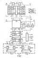
- the ternary signal to be regenerated - in the exemplary embodiment a pseudoternary AMI-coded signal A - is fed to two window comparators K1 and K2.
- the positive pulses of the signal A fall into the window of the comparator K1 and the negative into the window of the comparator K2.
- a binary one is present at the output of the comparator K1, while the output of the comparator K2 assumes the potential corresponding to a binary zero.
- a shift register SR1, SR2 is provided for each comparator, through which the binary samples are shifted with the clock f10 and transferred to a buffer S1, S2 in parallel with the clock f.
- the phase position of the symbol clock f, based on the signal A, can be any; therefore it is not necessary for the clock f to be recovered from the signal A. Any clock source with the nominal frequency of the symbol clock associated with signal A is sufficient.
- the clocks f10 and f have a time-independent phase relation to each other.
- SR1 which is just as large as the number of binary memory cells in the intermediate memories S1 and S2, is so large - namely 13 - that, regardless of the phase position of the clock f, 10 groups of four successive samples each -k is therefore too in the present example four have been elected - have space. In this way it is ensured that with each clock pulse of the clock f all samples of a signal element that fall into the eye of the signal A are in the buffer S1 or S2 as a seamless sequence. In addition, it is assumed that at least four samples of each signal element fall into the eye of signal A, the eye width as 6 is at least 2/5 of the nominal period of the symbol clock f.
- the purpose of the other circuit parts is, among other things, to automatically determine where the eye of the ternary signal A is located within the signal sections stored in the intermediate memories S1 and S2 and with each clock edge of the symbol clock f one of the sample values belonging to the eye from the intermediate memory S1 to the output AP or forward from the buffer S1 to the output AN.
- the binary ones in the buffer stores S1 and S2 are used to determine the position of the eye. If binary bars occur more frequently with the clock edges of the clock f on the same four successive memory cells of the buffer memories S1 or S2, these locations are regarded as the center of the eye of the signal A.
- the possible position of the center of the eye is determined by the logic L to which the buffer store S1 is connected via the connections E11 to E113 and the buffer store S2 via the connections E21 to E213.
- the exact structure of the logic L is shown in FIG. 2.
- the first four memory locations of the intermediate memory S1 are connected to the four inputs of an AND gate ULI via the connections E11 to E14.
- the memory cells 2 to 5 of the buffer S1 are connected via the connections E12 to E15 to the inputs of a further AND gate UL2 and so on to the memory locations 10 to 13, which have a tenth AND- via the connections E110 to E113 to the inputs.
- Gates UL10 are connected. The same applies to the connection of the memory locations of the buffer store S2 via the connections E21 to E213 to the AND gates UR1 to UR10.
- the outputs of the AND gates UL1 and UR1, which form a pair of gates, are connected to an OR gate OL1.
- a binary one occurs at the output of this OR gate OL1 if only binary ones are contained in the first four memory locations of the intermediate memory S1 or in the first four memory locations of the intermediate memory S2.
- the outputs of the OR gates OL1 to OL10 are at the same time the outputs of the logic L, they are connected via lines LS1 to LS10 to the inputs of a switching mechanism SW which is used to count how often binary at the outputs of the OR gates OL1 to OL10 Ones occur.
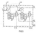
- FIG. 3 shows details of the switching mechanism SW - 10 counters Z1 to Z10 are provided, one of which is assigned to one of the OR gates OL1 to OL10 is. If a binary one occurs at the output of one of these OR gates at a clock instant of clock f, the assigned counter is incremented by one counter unit.
- switches SS1 to SS10 are provided, the control inputs of which are connected to one of the lines LS1 to LS10. A binary one on one of these lines closes the assigned switch, via which a clock pulse of the clock fs is then fed to the counter input of the connected counter.
- the clock fs is the symbol clock f which is phase-shifted by 90 °; the phase shift is necessary so that signal propagation times do not lead to malfunctions.
- the phase relation of all clocks used in the exemplary embodiment is shown schematically in the upper right part of FIG. 1.
- Each of the 4-stage counters Z1 to Z10 of the switching mechanism SW is provided with an interrogation circuit which consists of two AND gates.
- the first AND gate US1 to US10 is used to AND the three stages with the highest value of each counter Z1 to Z10.
- a binary one appears at the output of the AND gates US1 to US10 when the connected counter has reached a level of at least 14. These binary ones are led via lines AG1 to AG10 to the inputs of a third buffer S3 with ten storage locations.
- a binary one occurs at the output of the second AND gate UR1 to UR10 of each interrogation circuit as long as the connected counter is at its highest level, namely 15.
- the outputs of the second AND gates UR1 to UR10 are led via lines AW1 to AW10 to an OR gate 01 with ten inputs, at the output of which a binary one then occurs when at least one of the counters Z1 to Z10 has reached its maximum level.
- the output signal of the OR gate 01 is linked to the inverted symbol clock f by an AND gate U1, the output signal of which is used to clock the buffer store S3, into which the binary values on the lines AG1 to AG10 are adopted.
- a binary one in the memory locations of the intermediate store S3 indicates which of the counters Z1 to Z10 has reached status 14 or 15. Is this e.g. in the case of the counter Z10, this means that in the last four memory locations of the intermediate memory S1 or in the last four memory locations of the intermediate memory S2 there were only binary ones at 14 or 15 clock pulses of the symbol clock f.
- the signal sections which are buffered in the last four memory locations of the buffer memories S1 and S2 belong to the center of the eye of the signal A and the sample value stored in the memory location 13 of the buffer memory S1 becomes the output AP and the one stored in memory location 13 of the buffer memory S2 Sample placed at the output AN of the circuit of FIG. 1.
- the buffer S3 is followed by a selection circuit AWS, the inputs of which are connected via terminals BK1 to BK10 to the outputs of stages 1 to 10 of the buffer S3.
- An output is assigned to each input of the selection circuit AWS. If a binary one is present at several inputs of the selection circuit AWS, this is only forwarded to the assigned output at one input, while a binary zero is present at all other outputs.
- the binary values at the outputs of the selection circuit are led via lines AS1 to AS10 to the memory locations 1 to 10 of a fourth clocked buffer store S4, the function of which is explained in more detail below.
- a memory location other than the tenth memory location of the buffer memory S4 contains the binary one, then another of the AND gates UP1 to UP10 or UN1 to UN10 of the gate circuit GS is opened, and the stored binary values of other memory locations of the buffer memories S1 and S2 become passed to the outputs AP and AN for further processing.
- the search is repeated by deleting all counters as soon as a counter has reached its maximum level.
- the erase pulse for the counter is obtained from the output signal of the AND gate U1 and a clock Ts - which is phase-shifted by 270 ° with respect to the symbol clock f. Both signals become one em supplied another AND gate U2, the output of which is connected via a line RS to the reset inputs R of all counters Z1 to Z10.
- the content of the buffer S4 defines the storage locations of the buffer memories S1 and S2, the binary values of which are forwarded to the outputs AP and AN; it therefore determines the sampling phase of signal A.
- the eye of the signal A enlarged over time, the sampling phase position selected before the eye enlargement is just as suitable as e.g. a new phase sample position that would result solely from the functioning of the selection circuit AWS.
- a comparator VG with 20 inputs is provided, which are connected to terminals AK1 to AK10 and BK1 to BK10.
- the comparator VG only outputs a clock pulse to the buffer S4 if the sampling phase before changing the eye is not included in the permissible sampling phase after changing the eye, ie if none of the AND operations between the two signals at terminals AK1 and BK1 to AK10 and BK10 assume the value one. Only in this case are the binary values present at the output of the selection circuit AWS in the buffer S4 with the clock pulse of the comparator VG, the memory location in which the only binary one is stored determining the new sampling phase position.
Landscapes
- Engineering & Computer Science (AREA)
- Theoretical Computer Science (AREA)
- Power Engineering (AREA)
- Computer Networks & Wireless Communication (AREA)
- Signal Processing (AREA)
- Synchronisation In Digital Transmission Systems (AREA)
- Dc Digital Transmission (AREA)
- Stabilization Of Oscillater, Synchronisation, Frequency Synthesizers (AREA)
- Arrangements For Transmission Of Measured Signals (AREA)
- Measurement And Recording Of Electrical Phenomena And Electrical Characteristics Of The Living Body (AREA)
Priority Applications (1)
| Application Number | Priority Date | Filing Date | Title |
|---|---|---|---|
| AT86200957T ATE81571T1 (de) | 1985-06-04 | 1986-06-02 | Schaltungsanordnung zur abtastung eines ternaeren signales. |
Applications Claiming Priority (2)
| Application Number | Priority Date | Filing Date | Title |
|---|---|---|---|
| DE19853519929 DE3519929A1 (de) | 1985-06-04 | 1985-06-04 | Schaltungsanordnung zur abtastung eines ternaeren signales |
| DE3519929 | 1985-06-04 |
Publications (3)
| Publication Number | Publication Date |
|---|---|
| EP0204376A2 true EP0204376A2 (fr) | 1986-12-10 |
| EP0204376A3 EP0204376A3 (en) | 1989-01-04 |
| EP0204376B1 EP0204376B1 (fr) | 1992-10-14 |
Family
ID=6272359
Family Applications (1)
| Application Number | Title | Priority Date | Filing Date |
|---|---|---|---|
| EP86200957A Expired - Lifetime EP0204376B1 (fr) | 1985-06-04 | 1986-06-02 | Circuit pour l'exploration d'un signal ternaire |
Country Status (6)
| Country | Link |
|---|---|
| US (1) | US4700359A (fr) |
| EP (1) | EP0204376B1 (fr) |
| JP (1) | JPS61280146A (fr) |
| AT (1) | ATE81571T1 (fr) |
| CA (1) | CA1271531A (fr) |
| DE (2) | DE3519929A1 (fr) |
Cited By (1)
| Publication number | Priority date | Publication date | Assignee | Title |
|---|---|---|---|---|
| EP0556697A1 (fr) * | 1992-02-19 | 1993-08-25 | Siemens Aktiengesellschaft | Méthode et dispositif de transmission d'information auxiliaire |
Families Citing this family (7)
| Publication number | Priority date | Publication date | Assignee | Title |
|---|---|---|---|---|
| US4896334A (en) * | 1988-10-24 | 1990-01-23 | Northern Telecom Limited | Method and apparatus for timing recovery |
| USRE34206E (en) * | 1988-10-24 | 1993-03-30 | Northern Telecom Limited | Method and apparatus for timing recovery |
| US5157690A (en) * | 1990-10-30 | 1992-10-20 | Level One Communications, Inc. | Adaptive convergent decision feedback equalizer |
| DE4303962A1 (de) * | 1993-02-10 | 1994-08-18 | Georg Dipl Ing Figol | Datenregenerator |
| US6249557B1 (en) | 1997-03-04 | 2001-06-19 | Level One Communications, Inc. | Apparatus and method for performing timing recovery |
| US6167082A (en) * | 1997-03-06 | 2000-12-26 | Level One Communications, Inc. | Adaptive equalizers and methods for carrying out equalization with a precoded transmitter |
| DE19857396C2 (de) * | 1998-12-12 | 2002-11-14 | Josef Von Stackelberg | Ausfallsicherheitsgerichteter Binärstellenvergleicher mit ternärer Ergebnis- und Zustandsanzeige |
Family Cites Families (6)
| Publication number | Priority date | Publication date | Assignee | Title |
|---|---|---|---|---|
| US3864529A (en) * | 1972-09-14 | 1975-02-04 | Lynch Communication Systems | Receiver for decoding duobinary signals |
| US3764989A (en) * | 1972-12-20 | 1973-10-09 | Ultronic Systems Inc | Data sampling apparatus |
| US4080572A (en) * | 1976-11-24 | 1978-03-21 | Westinghouse Electric Corporation | Receiver and method for synchronizing and detecting coded waveforms |
| FR2377729A1 (fr) * | 1977-01-14 | 1978-08-11 | Thomson Csf | Dispositif de decodage de signaux numeriques, et systeme comportant un tel dispositif |
| DE2827958C2 (de) * | 1978-06-26 | 1980-07-17 | Siemens Ag, 1000 Berlin Und 8000 Muenchen | Streckenregenerator für in einem Partial-Response-Code vorliegende mehrstufige digitale Signale |
| US4339823A (en) * | 1980-08-15 | 1982-07-13 | Motorola, Inc. | Phase corrected clock signal recovery circuit |
-
1985
- 1985-06-04 DE DE19853519929 patent/DE3519929A1/de not_active Withdrawn
-
1986
- 1986-05-30 JP JP61123839A patent/JPS61280146A/ja active Pending
- 1986-06-02 AT AT86200957T patent/ATE81571T1/de not_active IP Right Cessation
- 1986-06-02 DE DE8686200957T patent/DE3686959D1/de not_active Expired - Lifetime
- 1986-06-02 EP EP86200957A patent/EP0204376B1/fr not_active Expired - Lifetime
- 1986-06-03 US US06/870,272 patent/US4700359A/en not_active Expired - Lifetime
- 1986-06-04 CA CA000510856A patent/CA1271531A/fr not_active Expired
Cited By (1)
| Publication number | Priority date | Publication date | Assignee | Title |
|---|---|---|---|---|
| EP0556697A1 (fr) * | 1992-02-19 | 1993-08-25 | Siemens Aktiengesellschaft | Méthode et dispositif de transmission d'information auxiliaire |
Also Published As
| Publication number | Publication date |
|---|---|
| EP0204376A3 (en) | 1989-01-04 |
| EP0204376B1 (fr) | 1992-10-14 |
| US4700359A (en) | 1987-10-13 |
| DE3519929A1 (de) | 1986-12-04 |
| CA1271531A (fr) | 1990-07-10 |
| JPS61280146A (ja) | 1986-12-10 |
| DE3686959D1 (de) | 1992-11-19 |
| ATE81571T1 (de) | 1992-10-15 |
Similar Documents
| Publication | Publication Date | Title |
|---|---|---|
| DE2047001B2 (de) | Anordnungen für die Übertragung von Daten innerhalb einer Datenverarbeitungsanlage | |
| EP0384936A1 (fr) | Procédé et dispositif pour transmettre des paquets d'information provenant de lignes d'entrée via un dispositif à communication de paquets | |
| DE2543130B2 (de) | Schaltungsanordnung zur Übertragung von digitalen Daten im VoUduplex-Betrieb zwischen wenigstens zwei Stationen | |
| DE2621882B2 (de) | Speicher für Rechenautomaten mit mindestens zwei parallel angeordneten, einen Rücklaufkreis aufweisenden Speicherschleifen | |
| DE1079100B (de) | Nachrichtenuebertragungssystem, insbesondere fuer Telegraphievermittlung | |
| DE1537248A1 (de) | Getasteter gleichstromgesteuerter bistabiler Multivibrator mit Vorzugslage bei gleichzeitiger Ansteuerung | |
| EP0204376B1 (fr) | Circuit pour l'exploration d'un signal ternaire | |
| DE2031038C3 (de) | Schaltungsanordnung zur Auswahl jeweils einer von 2" Adressenleitungen eines Speichersystems | |
| DE2822835B2 (de) | Schaltungsanordnung zur Eliminierung koinzidenter Impulse | |
| DE3213574C2 (de) | Schaltung zur Datenübertragung | |
| DE1964191A1 (de) | Zeitmultiplexanordnung | |
| DE3501274A1 (de) | Schalter | |
| DE2423195A1 (de) | Wartungsvorrichtung | |
| EP0141946B1 (fr) | Dispositif pour la synchronisation des flancs de signaux binaires avec un signal d'horloge | |
| EP0173274B1 (fr) | Méthode et montage pour la réalisation et la maintenance d'une liaison à division temporelle à large bande | |
| EP0021084B1 (fr) | Mémoire intégrée monolithique à semi-conducteurs | |
| DE2846624A1 (de) | Binaerer signaldetektor fuer zeichenerkennungseinrichtungen | |
| DE4422784C2 (de) | Schaltungsanordnung mit wenigstens einer Schaltungseinheit wie einem Register, einer Speicherzelle, einer Speicheranordnung oder dergleichen | |
| EP0166274A2 (fr) | Dispositif pour la détection d'un motif de bits prédéterminé dans des signaux binaires apparaissant en série | |
| DE2335408C2 (de) | Schaltungsanordnung zur Realisierung einer Oderfunktion bei der Übertragung schneller digitaler Signale über lange Leitungen | |
| DE3246211C2 (de) | Schaltungsanordnung zur Detektion von Folgen identischer Binärwerte | |
| DE2339008A1 (de) | Einrichtung zur datenvermittlung und datensicherung in zeitvielfach-vermittlungsnetzen | |
| EP0334193B1 (fr) | Méthode et dispositif pour l'ajustement continu de la phase d'un signal de données numériques d'une horloge | |
| DE2430760A1 (de) | Hdb3-codec | |
| EP0042621B1 (fr) | Régénérateur pour signaux numériques multiniveaux |
Legal Events
| Date | Code | Title | Description |
|---|---|---|---|
| PUAI | Public reference made under article 153(3) epc to a published international application that has entered the european phase |
Free format text: ORIGINAL CODE: 0009012 |
|
| AK | Designated contracting states |
Kind code of ref document: A2 Designated state(s): AT BE CH DE FR GB IT LI NL SE |
|
| RAP1 | Party data changed (applicant data changed or rights of an application transferred) |
Owner name: N.V. PHILIPS' GLOEILAMPENFABRIEKEN Owner name: PHILIPS PATENTVERWALTUNG GMBH |
|
| PUAL | Search report despatched |
Free format text: ORIGINAL CODE: 0009013 |
|
| AK | Designated contracting states |
Kind code of ref document: A3 Designated state(s): AT BE CH DE FR GB IT LI NL SE |
|
| 17P | Request for examination filed |
Effective date: 19890626 |
|
| 17Q | First examination report despatched |
Effective date: 19910718 |
|
| GRAA | (expected) grant |
Free format text: ORIGINAL CODE: 0009210 |
|
| AK | Designated contracting states |
Kind code of ref document: B1 Designated state(s): AT BE CH DE FR GB IT LI NL SE |
|
| PG25 | Lapsed in a contracting state [announced via postgrant information from national office to epo] |
Ref country code: NL Effective date: 19921014 Ref country code: BE Effective date: 19921014 |
|
| REF | Corresponds to: |
Ref document number: 81571 Country of ref document: AT Date of ref document: 19921015 Kind code of ref document: T |
|
| REF | Corresponds to: |
Ref document number: 3686959 Country of ref document: DE Date of ref document: 19921119 |
|
| ITF | It: translation for a ep patent filed | ||
| ET | Fr: translation filed | ||
| GBT | Gb: translation of ep patent filed (gb section 77(6)(a)/1977) |
Effective date: 19930111 |
|
| NLV1 | Nl: lapsed or annulled due to failure to fulfill the requirements of art. 29p and 29m of the patents act | ||
| PG25 | Lapsed in a contracting state [announced via postgrant information from national office to epo] |
Ref country code: AT Effective date: 19930602 |
|
| PG25 | Lapsed in a contracting state [announced via postgrant information from national office to epo] |
Ref country code: LI Effective date: 19930630 Ref country code: CH Effective date: 19930630 |
|
| PLBE | No opposition filed within time limit |
Free format text: ORIGINAL CODE: 0009261 |
|
| STAA | Information on the status of an ep patent application or granted ep patent |
Free format text: STATUS: NO OPPOSITION FILED WITHIN TIME LIMIT |
|
| 26N | No opposition filed | ||
| REG | Reference to a national code |
Ref country code: CH Ref legal event code: PL |
|
| ITTA | It: last paid annual fee | ||
| EAL | Se: european patent in force in sweden |
Ref document number: 86200957.8 |
|
| ITPR | It: changes in ownership of a european patent |
Owner name: CAMBIO RAGIONE SOCIALE;PHILIPS ELECTRONICS N.V. |
|
| REG | Reference to a national code |
Ref country code: GB Ref legal event code: 732E |
|
| REG | Reference to a national code |
Ref country code: FR Ref legal event code: TP |
|
| REG | Reference to a national code |
Ref country code: GB Ref legal event code: IF02 |
|
| PGFP | Annual fee paid to national office [announced via postgrant information from national office to epo] |
Ref country code: SE Payment date: 20020416 Year of fee payment: 17 |
|
| PGFP | Annual fee paid to national office [announced via postgrant information from national office to epo] |
Ref country code: FR Payment date: 20020524 Year of fee payment: 17 |
|
| PGFP | Annual fee paid to national office [announced via postgrant information from national office to epo] |
Ref country code: GB Payment date: 20020527 Year of fee payment: 17 |
|
| PGFP | Annual fee paid to national office [announced via postgrant information from national office to epo] |
Ref country code: DE Payment date: 20020628 Year of fee payment: 17 |
|
| PG25 | Lapsed in a contracting state [announced via postgrant information from national office to epo] |
Ref country code: GB Free format text: LAPSE BECAUSE OF NON-PAYMENT OF DUE FEES Effective date: 20030602 |
|
| PG25 | Lapsed in a contracting state [announced via postgrant information from national office to epo] |
Ref country code: SE Free format text: LAPSE BECAUSE OF NON-PAYMENT OF DUE FEES Effective date: 20030603 |
|
| PG25 | Lapsed in a contracting state [announced via postgrant information from national office to epo] |
Ref country code: DE Free format text: LAPSE BECAUSE OF NON-PAYMENT OF DUE FEES Effective date: 20040101 |
|
| GBPC | Gb: european patent ceased through non-payment of renewal fee |
Effective date: 20030602 |
|
| EUG | Se: european patent has lapsed | ||
| PG25 | Lapsed in a contracting state [announced via postgrant information from national office to epo] |
Ref country code: FR Free format text: LAPSE BECAUSE OF NON-PAYMENT OF DUE FEES Effective date: 20040227 |
|
| REG | Reference to a national code |
Ref country code: FR Ref legal event code: ST |
|
| PG25 | Lapsed in a contracting state [announced via postgrant information from national office to epo] |
Ref country code: IT Free format text: LAPSE BECAUSE OF NON-PAYMENT OF DUE FEES Effective date: 20050602 |