EP0205020A2 - Tragbares elektronisches Notizgerät - Google Patents
Tragbares elektronisches Notizgerät Download PDFInfo
- Publication number
- EP0205020A2 EP0205020A2 EP86107112A EP86107112A EP0205020A2 EP 0205020 A2 EP0205020 A2 EP 0205020A2 EP 86107112 A EP86107112 A EP 86107112A EP 86107112 A EP86107112 A EP 86107112A EP 0205020 A2 EP0205020 A2 EP 0205020A2
- Authority
- EP
- European Patent Office
- Prior art keywords
- data
- password
- secret
- mode
- memory
- Prior art date
- Legal status (The legal status is an assumption and is not a legal conclusion. Google has not performed a legal analysis and makes no representation as to the accuracy of the status listed.)
- Granted
Links
Images





Classifications
-
- G—PHYSICS
- G06—COMPUTING OR CALCULATING; COUNTING
- G06F—ELECTRIC DIGITAL DATA PROCESSING
- G06F21/00—Security arrangements for protecting computers, components thereof, programs or data against unauthorised activity
- G06F21/70—Protecting specific internal or peripheral components, in which the protection of a component leads to protection of the entire computer
- G06F21/78—Protecting specific internal or peripheral components, in which the protection of a component leads to protection of the entire computer to assure secure storage of data
-
- G—PHYSICS
- G06—COMPUTING OR CALCULATING; COUNTING
- G06F—ELECTRIC DIGITAL DATA PROCESSING
- G06F15/00—Digital computers in general; Data processing equipment in general
- G06F15/02—Digital computers in general; Data processing equipment in general manually operated with input through keyboard and computation using a built-in program, e.g. pocket calculators
- G06F15/025—Digital computers in general; Data processing equipment in general manually operated with input through keyboard and computation using a built-in program, e.g. pocket calculators adapted to a specific application
- G06F15/0283—Digital computers in general; Data processing equipment in general manually operated with input through keyboard and computation using a built-in program, e.g. pocket calculators adapted to a specific application for data storage and retrieval
-
- G—PHYSICS
- G06—COMPUTING OR CALCULATING; COUNTING
- G06F—ELECTRIC DIGITAL DATA PROCESSING
- G06F21/00—Security arrangements for protecting computers, components thereof, programs or data against unauthorised activity
- G06F21/30—Authentication, i.e. establishing the identity or authorisation of security principals
- G06F21/31—User authentication
-
- G—PHYSICS
- G06—COMPUTING OR CALCULATING; COUNTING
- G06F—ELECTRIC DIGITAL DATA PROCESSING
- G06F21/00—Security arrangements for protecting computers, components thereof, programs or data against unauthorised activity
- G06F21/70—Protecting specific internal or peripheral components, in which the protection of a component leads to protection of the entire computer
- G06F21/78—Protecting specific internal or peripheral components, in which the protection of a component leads to protection of the entire computer to assure secure storage of data
- G06F21/79—Protecting specific internal or peripheral components, in which the protection of a component leads to protection of the entire computer to assure secure storage of data in semiconductor storage media, e.g. directly-addressable memories
-
- G—PHYSICS
- G06—COMPUTING OR CALCULATING; COUNTING
- G06F—ELECTRIC DIGITAL DATA PROCESSING
- G06F2221/00—Indexing scheme relating to security arrangements for protecting computers, components thereof, programs or data against unauthorised activity
- G06F2221/21—Indexing scheme relating to G06F21/00 and subgroups addressing additional information or applications relating to security arrangements for protecting computers, components thereof, programs or data against unauthorised activity
- G06F2221/2105—Dual mode as a secondary aspect
Definitions
- This invention relates to a portable electronic memorandum device with a data memory which allows reading/writing of character data items such as names, telephone numbers, addresses, schedules and the like.
- Recent commercially available electronic wrist watches, small electronic calculators, etc. are usually provided with time display and calculating functions.
- Some of this type of electronic devices additionally have a so-called data bank function.
- These devices with the data bank function have memories for storing item data such as names, telephone numbers, and schedules. Users can read out desired item data from the memories at any time.
- this type of electronic devices have usually secret function for protecting such data from being stolen by other persons. To this end, this device uses passwords, or secret words, without by which the item data cannot be read out.
- U.S. Patent No. 4117542 discloses two types of the data bank electronic device with the so-called secret function.
- the first type of the electronic device user presets secret codes of his own in RAM of the device. For reading out desired data later, he enters the secret code associated with that data, which been preset.
- secret codes In the second data bank electronic device, secret codes have been fixed in the ROM at the factory. User uses these fixed secret codes later for his desired data retrieval through appropriate keyboard operation.
- the second type electronic device in which secret codes have been stored in the manufacturing stage, has disadvantages. For example, if user forgets the password, he cannot use the memory area of the device unless he can recall the password or find it out from the maker.
- the first type of the electronic device in which the user himself enters the password data into the RAM, has the following disadvantages. If the user, with a specified device model, sets the password data, for example, by key operation, it is naturally set with the procedure specified for that model. If the model device being operated by the user is one widely marketed in great numbers, the password data setting, cancellation, and change procedures for that model will be known by many people. As a result, even though the password is supposed to be secret, the cancellation and change of the password can be very easily performed by other persons, and there is danger that the secrecy will not be maintained.
- an object of this invention is to provide a portable electronic memorandum device which enables the user to make an access to the memory even if he forgets the password for privately accessing the memory, while keeping the secrecy of the data stored.
- a portable electronic memorandum device comprising:
- FIG. 1 there is shown an electronic wrist watch with data bank function to which the present invention is applied.
- Keyboard 1 and display device 2 are located on the face of this electronic wrist watch.
- Display device 2 displays the time, data, etc. and also selectively displays the password data (secret code) when the password data (secret code) is set or key operation is made. Further, pages of data composed of person's names and their telephone numbers are displayed successively.
- Keyboard 1 has page feed keys SP1 and SP2 besides every kind of alphabetic and numeric operational keys. In a data bank mode to be given later, these keys cause each display device 2 to change the displayed contents page by page. Key SP1 causes the display device to display the next page, while page SP2 causes it to display the preceding page. Switches Sl to S3, and Sc are provided on the sides of the watch case. Switch S3 is a mode select switch for selecting either the data bank mode or a watch mode. Switch S2 selects either a write mode or a read mode when the electronic device is in the data bank mode. In this instance, the item data such as people's names and addresses consists of secret data which cannot be displayed without entering the password data, and normal data which can be displayed at will.
- the item data such as people's names and addresses consists of secret data which cannot be displayed without entering the password data, and normal data which can be displayed at will.
- Switch Sl is a double-function key. In a readout (display) mode for data bank, it switches the mode between the normal mode for reading out normal data and the secret mode for reading out secret data. In the write mode for data bank, it serves as a correction digit select key. Switch Sc is a clear key for clearing the secret data.
- Fig. 15 shows a layout of display figures on the display device 2. These display figures are made of liquid crystal.
- a main digital display section 2A including eight digits of numeral 8 shaped figures is located in the lower part of the display device 2. Laid out in the upper part are a sub digital display section 2B made up of four digits of numeral 8 shaped figures, a matrix display section 2C of five digits, AM and PM indicators, and a secret mode mark indicator 2D. These sections and indicators are laid out in this order from right to left as viewed in the drawing.
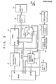
- ROM 11 stores a microprogram for controlling all the operations of the wrist watch, and provides microinstructions OP, DO and NA in a parallel fashion.
- Microinstruction OP is transferred to instruction decoder 12. The decoder decodes this instruction to transfer it as a data read command or a write command to the input terminal R/W of RAM (random access memory) 13, and as an operation command to the input terminal S of arithmetic/logic unit (ALU) 14.
- ALU arithmetic/logic unit
- Microinstruction DO is input as address data to the input terminal Adder of RAM 13, and as numerical data to the input terminal of DI2 of arithmetic/logic unit 14. Further, it is input to address control unit 15.
- Microinstruction NA is the next address data to be input to address control unit 15, whose output is input to the input terminal Adder of ROM 11.
- RA M 13 includes registers for temporarily storing data and for operating data, and are used for clock, key-in and operation processings, and the like. It is operated under control of instruction decoder 12.
- the data read out DO from RAM 13 is applied to the input terminal DI1 and DI2 of ALU 14, and is displayed by display unit 17 under control of display control unit 16.
- ALU 14 executes various types of operations. Data representing result of operation is applied to the input terminal DI of RAM 13, and loaded into the memory.
- ALU 14 outputs a signal representative of presence or absence of the operation result data and of carrier, and applies it to address control unit 15. Finally, it changes the address in ROM 11.
- Address control unit 15 is applied with a clock signal at 16 Hz, which is formed by appropriately frequency dividing the reference clock signal from oscillator 18 by frequency divider 19. According to this 16 Hz signal, the clock processing is executed with the interrupt every 1/16 second.
- a signal at a predetermined frequency as output from frequency divider 19 is applied to timing generator 20 and causes it to produce various types of timing signals, which are applied to related circuits.
- Key codes output from key-in unit 21 are applied to the input terminal DI2 of ALU 14.
- Fig. 4 shows a memory map of RAM 13.
- RAM 13 has a memory area for storing clock data, system control data, and item data such as names and telephone numbers, which can freely be written and read out through the key operation by the user.
- register T is for storing current time.
- Register D is for storing date.
- Password memory section Z stores preset 4-digit passwords.
- Data memory DM stores various types of item data for data bank such as normal data and secret data.
- Memory A stores all items of normal data as stored in this data memory DM.
- Memory B stores all items of secret data as stored in data memory DM.
- Normal display page pointer AD stores the displayed page number of the normal data.
- RAM 13 is further provided with secret display page pointer BD for storing the displayed page number of secret data, and flag registers Ff, Fq and Fs.
- Data memory DM can store item data up to 50 pages corresponding to the digits "1" to "50".
- Data memory DM consists of 50 memory addresses, whose memory areas can store a maximum of 50 pages of item data. Normal data is stored from address No.1 in numerical sequence. Secret data is stored starting at address No. 50, in reverse numerical sequence.
- the number of addresses having normal and secret data as stored are not necessarily divided equally (25 and 25), but differ according to the quantity of each type of data. For example, if there are 30 pages of normal data, there is only room for 20 pages of secret data, because the maximum total number of addresses in the memory is 50.
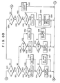
- Figs. 5 to 7 show flowcharts describing the operations.
- Fig. 7 illustrates the states of displays which are changed by the operation switches.
- step Sl the memorandum device remains in a standby state until it is required by watch timing or key-in.
- a clock signal of 16 Hz is output from frequency divider 19
- the control by CPU proceeds to step S2, and clock processing is executed.
- step S3 the alarm processing of step S3 is executed.
- a key code corresponding to the operated key is output from key-in unit 21
- a key processing program as specified by this key code is specified, and key processing and display processing are executed by step S4.
- Figs. 6A through 6C show flowcharts illustrating in detail the key processing and display processing of step 4 of Fig. 5.
- step Sll When the mode is changed from clock mode to data bank mode or vice versa by operating switch S3, this change is detected in step Sll.
- register Fs is cleared in step S13.
- Register Fs stores a flag indicating the secret mode or the normal mode. When the contents of Fs are "I”, the secret mode is specified, and when it is "0", the normal mode is specified. Accordingly, after a mode change is accompalished by operation of the switch S3, register Fs is automatically placed in the "0" or normal mode.
- the control flows from step Sll through step S14 for mode check and proceeds to step S15. In this step S15, the processing as specified by the operated key in the clock mode, such as correction processing and alarm time setting processing .is performed.
- Step S16 checks (judges) if switch S2 has been operated or not. Switch S2 is used to select either the read out mode or write mode in the data bank mode. If step S16 confirms that switch S2 has been operated, step S17 check, according to the contents of register Ff, if the present mode is the read out mode or the write mode. If the contents of register Ff are "1", the write mode is valid, and if they are "0", the read out mode is valid. If the write mode is specified, register Ff is cleared in step S18, and the read out mode is set up. If the read out mode is set up, the control of step S19 sets "1" to register Ff to set up the write mode.
- step S21 when the read out mode for the data bank is set up, viz. "0" is set in register Ff, if page feed key S is operated, the operation of key SP is checked and the control advances to step S21.
- the mode of the device is checked if it is normal or secret, the normal data is cyclically read out page by page from data memory DM of RAM 13 every time switch SP1 is operated, and displayed. This is because the device has been set in the normal mode in step S13.
- the display page of the normal data stored in normal display page pointer Ad is compared with all items of normal data as stored in memory A.
- step S23 increments by one the display page number of normal display number pointer AD.
- the normal data is still stored in the data memory DM.
- step S24 the control goes to step S27.
- step S27 the normal data corresponding to the display page number is read out and displayed.
- step S25 is executed and the blank display is made to indicate blank page. Under this condition, if switch SP1 is further operated, the controls goes from step S22 to step S26. In this step, "1" is set to normal display page pointer AD. The first normal data is read out and displayed.
- the block X enclosed by the broken line in Fig. 7 indicates the displays in the normal data read out mode.
- the normal data is successively read out from data memory DM in the direction of address "1" to "50", and is displayed successively.
- the next switch operation of switch SP1 causes the blank display.
- the additional switch operation of switch SP1 causes the display to display the first normal data. In this way, the normal data is cyclically displayed.
- step S28 the secret data is read out in the direction from the address "50" to address 21" of data memory DM. Accordingly, the contents of secret display page pointer BD are decremented by one every time switch SPl is operated.
- step S32 to cyclically display normal data, the contents at address "50" are set in secret display page pointer BD.
- the block Y enclosed by broken line in Fig. 7 shows the displays in the secret data read out mode. Every time switch SP1 is operated, the secret data is successively read out in the order from address "50" to address "1" of data memory DM, and is displayed in successive manner.
- the blank display is made by operation of switch SPl.
- a further operation of switch SP1 causes the display to display the first secret data.
- step S34 check is made if the mode set up is write mode or read out mode for data bank.
- step S36 further checks if the mode is the normal mode or the secret mode. Since the present mode is in the normal data read out mode, the control proceeds to step S18.
- This step sets "1" in register Fq. This register is for storing a flag showing permission or prohibition of inputting the password is set in register Fq. "1" of the flag specifies password input permission, while "0" of the flag specifies the password input prohibition.
- step S39 the display for password input permission is performed.
- the block Z-1 in Fig. 7 shows the display at this time.
- This display contains the display (No ?) to specify the inputting of the password, and the display of cursor "-" corresponding to each digit for showing input digits (4 digits) as well.
- the display for the first digit flickers at 1 Hz.
- Step S41 checks if clear switch Sc is cleared.
- step S47 This step checks if the password input is permitted on the basis of the contents of register Fq.
- switch Sl is operated in the normal data read out mode, and hence the password is placed in the input permission state. Therefore, the control goes to step S48 where one character input processing is performed.
- the first data as input in step S48 is displayed as the first digit data of the password in step S49.
- step S50 check is made whether or not all digits of the password (four digits in this instance) have been input. Since the first digit is input in the first place, the sequence of processings from step S41 to S44 are repeated until all of the digits have been input.
- step S51 Upon completion of the password inputting, step S51 checks if the password is stored (registered) in the password memory Z in RAM 13. If it is registered, step S52 compares the password stored in password memory Z with the input password to check if these are coincident with each other. If these are not coincident with each other, register Fq is cleared in the next step S53 and the password input prohibition state is set up. In the next step S54, "ERROR" is displayed, as shown in the block Z-3 in F ig. 7. If the register password and the input password are coincident with each other, "1" is set in register Fs in step S55 to change the mode from the normal mode to the secret mode.
- the secret mode in the normal mode, is automatically changed through the procedure that following the operation of switch Sl, the password is input, and CPU considers that it is correct.
- register Fq is cleared, and the password prohibition state is set up.
- "K" is displayed, as shown by the block Z-2 in Fig. 7.
- step S51 if CPU confirms that the password is not yet registered, the 4-digit numerical data as input in step S58 is sent to and stored in password memory Z of RAM 13. Further, in step S59, register Fq is cleared.
- register Fs contains "1" and the mode is automatically changed to the secret mode. Further, when switch SPl is operated, the control advances from step S21 to step S28, allowing the secret data to be read out. If the input error of the password is detected, no mode change to the secret mode occurs, so that the secret data can not be read out.
- the secret data stored in the secret area of RAM can not be read out by other persons than the person who knows the password.
- only the owner of the wrist watch who sets the password can read out the secret data for display, thereby to keep the secrecy of his private data.
- step S41 the control advances from step S41 to S42 where check is made if the mode is the write mode or read mode, on the basis of the contents of register Ff. Since the present mode of the electronic memorandum device is the read out mode, the control goes to step S43. In this step, the memory B in RAM 13 is cleared, so that all items of secret data are all "0's". Subsequently, in step S44, "1" is set in register Fs. In the next step S45, the password memory Z of RAM 13 is cleared. In step S46, the blank display is performed.
- the block YC in Fig. 7 shows the display at this time.
- the mode is changed to the secret mode by the operation of clear switch Sc.
- all items of the secret data are cleared.
- page change key SP1 is operated, the display is left in the blank display.
- page feed key SP1 is operated when memory B is cleared, the control starts at step S 20, proceeds through steps S21 and S28 to step S32.
- the display page number of secret data is necessary "50".
- the control proceeds from step S30 to step S31, to keep the blank display.
- clear switch Sc is operated, the read out of the secret data is prohibited and the secret data area of data memory DM is cleared.
- step S37 the control proceeds to step S37 through steps S35 to S36.
- register Fs is cleared to set up the normal mode.
- steps S38 and S39 are not executed.
- step S2 in the data bank mode, by operating switch S2, "1" is set to register Ff to set up the write mode.
- this write mode ten keys are operated to enter telephone numbers, and alphabet keys are operated to enter names.
- step S41 the control advances from step S41 to step 47.
- register Fq is still in the password inhibition state. Therefore, the control proceeds to step S60. In this step, check is made if the mode is the read out mode or the write mode on the basis of the contents of register Ff.
- step S61 the character entering is executed in the next step S61.
- step S62 the characters entered are each displayed at the digit position corresponding to the displayed cursor position.
- step S64 the entered characters are stored into the data memory DM area, which corresponds to the normal display page of the normal display pointer.
- step S65 is executed to enter input characters into the memory area of data memory DM, which corresponds to the secret display page of secret display page pointer BD. In this way, the data of one page is performed.
- page feed key S P 1 is operated to alter the contents of normal display page pointer AD or secret display page pointer BD. Further, ten keys and alphabet keys are operated to enter the data of one page. In this way, both of the normal data and secret data can be written into the memory.
- the contents of memory B for storing all items of secret data are cleared.
- "0 0 " is written into the memory area for secret data, and then is cleared.
- the secret data has been explained as being optically displayed on liquid crystal display device 2, it may be printed out by, for example, a printer.
- This invention can be applied not only to an electronic timepiece as set forth above, but also to any proper device, such as a disk time-keeper, compact type electronic calculator, and IC card. It should be understood that the present invention is not limited to the above-mentioned embodiments, but may variously be changed and modified within the scope of this invention.
Landscapes
- Engineering & Computer Science (AREA)
- Theoretical Computer Science (AREA)
- Computer Security & Cryptography (AREA)
- Computer Hardware Design (AREA)
- Physics & Mathematics (AREA)
- General Engineering & Computer Science (AREA)
- General Physics & Mathematics (AREA)
- Software Systems (AREA)
- Computing Systems (AREA)
- Calculators And Similar Devices (AREA)
- Storage Device Security (AREA)
Priority Applications (1)
| Application Number | Priority Date | Filing Date | Title |
|---|---|---|---|
| EP90115387A EP0402961B1 (de) | 1985-05-31 | 1986-05-26 | Tragbares elektronisches Notizgerät |
Applications Claiming Priority (2)
| Application Number | Priority Date | Filing Date | Title |
|---|---|---|---|
| JP117746/85 | 1985-05-31 | ||
| JP60117746A JPS61275948A (ja) | 1985-05-31 | 1985-05-31 | デ−タ記憶装置 |
Related Child Applications (2)
| Application Number | Title | Priority Date | Filing Date |
|---|---|---|---|
| EP90115387.4 Division-Into | 1986-05-26 | ||
| EP90115387A Division EP0402961B1 (de) | 1985-05-31 | 1986-05-26 | Tragbares elektronisches Notizgerät |
Publications (3)
| Publication Number | Publication Date |
|---|---|
| EP0205020A2 true EP0205020A2 (de) | 1986-12-17 |
| EP0205020A3 EP0205020A3 (en) | 1988-01-27 |
| EP0205020B1 EP0205020B1 (de) | 1991-09-18 |
Family
ID=14719283
Family Applications (3)
| Application Number | Title | Priority Date | Filing Date |
|---|---|---|---|
| EP86107112A Expired EP0205020B1 (de) | 1985-05-31 | 1986-05-26 | Tragbares elektronisches Notizgerät |
| EP96115149A Expired - Lifetime EP0758109B1 (de) | 1985-05-31 | 1986-05-26 | Verfahren zum Verarbeiten und Vergleichen eines Kennworts |
| EP90115387A Expired - Lifetime EP0402961B1 (de) | 1985-05-31 | 1986-05-26 | Tragbares elektronisches Notizgerät |
Family Applications After (2)
| Application Number | Title | Priority Date | Filing Date |
|---|---|---|---|
| EP96115149A Expired - Lifetime EP0758109B1 (de) | 1985-05-31 | 1986-05-26 | Verfahren zum Verarbeiten und Vergleichen eines Kennworts |
| EP90115387A Expired - Lifetime EP0402961B1 (de) | 1985-05-31 | 1986-05-26 | Tragbares elektronisches Notizgerät |
Country Status (5)
| Country | Link |
|---|---|
| US (1) | US4815032A (de) |
| EP (3) | EP0205020B1 (de) |
| JP (1) | JPS61275948A (de) |
| DE (3) | DE3650704T2 (de) |
| HK (2) | HK58096A (de) |
Cited By (5)
| Publication number | Priority date | Publication date | Assignee | Title |
|---|---|---|---|---|
| EP0264098A3 (en) * | 1986-10-14 | 1990-11-22 | Sharp Kabushiki Kaisha | Input system for use in a portable type data processing device |
| EP0298242A3 (de) * | 1987-05-27 | 1991-07-03 | Sharp Kabushiki Kaisha | Elektronische Einrichtung, geeignet zum Speichern geheimer Daten |
| EP0351791A3 (de) * | 1988-07-20 | 1991-10-30 | Casio Computer Company Limited | Automatischer Wählapparat |
| US5119417A (en) * | 1988-07-20 | 1992-06-02 | Casio Computer Co., Ltd. | Auto-dialing apparatus |
| GB2288676A (en) * | 1994-04-22 | 1995-10-25 | Sharp Kk | Information retrieving apparatus |
Families Citing this family (17)
| Publication number | Priority date | Publication date | Assignee | Title |
|---|---|---|---|---|
| US5204840A (en) * | 1989-08-08 | 1993-04-20 | Mazur Jeffrey G | Means and methods for preserving microprocessor memory |
| US5313639A (en) * | 1992-06-26 | 1994-05-17 | George Chao | Computer with security device for controlling access thereto |
| JPH06236325A (ja) * | 1993-02-08 | 1994-08-23 | Sansei Denshi Japan Kk | データ記憶装置 |
| NL9301880A (nl) * | 1993-11-02 | 1995-06-01 | Robert Eric Hertzberger | Werkwijze en inrichting voor de opslag van gegevens in het bijzonder pincodes. |
| JPH0830749A (ja) * | 1994-07-13 | 1996-02-02 | Mitsubishi Electric Corp | 非接触icカード |
| US5644444A (en) * | 1995-03-10 | 1997-07-01 | Iomega Corporation | Read/write protect scheme for a disk cartridge and drive |
| US6724554B1 (en) | 1995-03-10 | 2004-04-20 | Iomega Corporation | Read/write protect scheme for a disk cartridge and drive |
| JP2957938B2 (ja) * | 1995-03-31 | 1999-10-06 | ミツビシ・エレクトリック・インフォメイション・テクノロジー・センター・アメリカ・インコーポレイテッド | ウインドウ制御システム |
| US5896255A (en) * | 1995-10-02 | 1999-04-20 | Aris Mardirossian, Inc. | Magnetic disc cartridge and corresponding system/method for limiting coping of software |
| JP3764961B2 (ja) * | 1995-11-30 | 2006-04-12 | カシオ計算機株式会社 | シークレットデータ記憶装置及びシークレットデータの読み出し方法 |
| US5872515A (en) * | 1996-03-20 | 1999-02-16 | Samsung Electronics Co., Ltd. | Laptop computer with an anti-theft alarm function and a method of controlling the same |
| JPH117420A (ja) * | 1997-04-22 | 1999-01-12 | Sharp Corp | データ受信装置 |
| US6003473A (en) * | 1998-02-12 | 1999-12-21 | Printz; Robert L. | Pet identification and retrieval device |
| US6720860B1 (en) * | 2000-06-30 | 2004-04-13 | International Business Machines Corporation | Password protection using spatial and temporal variation in a high-resolution touch sensitive display |
| US20030110046A1 (en) * | 2001-12-06 | 2003-06-12 | Nokia Corporation | Method and device for dispensing electronic information |
| JP4618103B2 (ja) * | 2005-11-11 | 2011-01-26 | セイコーエプソン株式会社 | 情報表示装置 |
| US8838995B2 (en) * | 2009-05-29 | 2014-09-16 | Western Digital Technologies, Inc. | Physically modifying a data storage device to disable access to secure data and repurpose the data storage device |
Family Cites Families (24)
| Publication number | Priority date | Publication date | Assignee | Title |
|---|---|---|---|---|
| SE381940B (sv) * | 1972-04-11 | 1975-12-22 | Gretag Ag | Anordning for enskild identifiering av ett flertal individer |
| US4005386A (en) * | 1974-05-21 | 1977-01-25 | Canon Kabushiki Kaisha | Clearing system |
| US4262337A (en) * | 1974-09-03 | 1981-04-14 | General Motors Corporation | Portable calculator incorporating an anti-theft feature |
| US3999050A (en) * | 1975-10-10 | 1976-12-21 | Pitroda Satyan G | Electronic diary |
| US4139893A (en) * | 1977-04-01 | 1979-02-13 | Texas Instruments Incorporated | Calculator program security system |
| US4181963A (en) | 1977-04-19 | 1980-01-01 | Casio Computer Co., Ltd. | Electronic calculator with time counting function |
| US4279022A (en) * | 1977-05-14 | 1981-07-14 | Tokyo Shibaura Electric Co., Ltd. | Electronic calculation/memorandum apparatus |
| FR2392447A1 (fr) * | 1977-05-26 | 1978-12-22 | Cii Honeywell Bull | Systeme de traitement d'informations protegeant le secret d'informations confidentielles |
| US4117542A (en) * | 1977-07-07 | 1978-09-26 | Judah Klausner | Electronic pocket directory |
| US4402056A (en) * | 1978-01-31 | 1983-08-30 | Canon Kabushiki Kaisha | Electronic digital memorandum |
| US4274146A (en) | 1978-06-12 | 1981-06-16 | Casio Computer Co., Ltd. | Calendar data display device for an electronic device |
| FR2455320B1 (fr) * | 1979-04-25 | 1986-01-24 | Cii Honeywell Bull | Dispositif de recyclage de supports d'enregistrement identifiables a l'aide de donnees d'identification et composes de memoires monolithiques non volatiles effacables |
| US4325089A (en) * | 1979-12-10 | 1982-04-13 | Hsu Da L | System for safeguarding magnetically recorded data |
| US4357529A (en) * | 1980-02-04 | 1982-11-02 | Atalla Technovations | Multilevel security apparatus and method |
| US4388695A (en) * | 1980-02-21 | 1983-06-14 | Timeplex, Inc. | Hardware memory write lock circuit |
| JPS576959A (en) * | 1980-06-13 | 1982-01-13 | Sharp Corp | Electronic memorandum device |
| US4736373A (en) * | 1981-08-03 | 1988-04-05 | Pacific Western Systems, Inc. | Memory tester having concurrent failure data readout and memory repair analysis |
| US4521853A (en) * | 1982-06-30 | 1985-06-04 | Texas Instruments Incorporated | Secure microprocessor/microcomputer with secured memory |
| JPS5930159A (ja) * | 1982-08-11 | 1984-02-17 | Citizen Watch Co Ltd | シ−クレツトメモリ−装置 |
| US4512453A (en) * | 1982-09-24 | 1985-04-23 | Umc Industries, Inc. | Vendor accountability system |
| WO1984004614A1 (en) * | 1983-05-13 | 1984-11-22 | Ira Dennis Gale | Data security device |
| US4573119A (en) * | 1983-07-11 | 1986-02-25 | Westheimer Thomas O | Computer software protection system |
| US4494114B1 (en) * | 1983-12-05 | 1996-10-15 | Int Electronic Tech | Security arrangement for and method of rendering microprocessor-controlled electronic equipment inoperative after occurrence of disabling event |
| GB2173738B (en) * | 1985-04-19 | 1989-07-12 | Roneo Alcatel Ltd | Secure transport of information between electronic stations |
-
1985
- 1985-05-31 JP JP60117746A patent/JPS61275948A/ja active Pending
-
1986
- 1986-05-23 US US06/867,244 patent/US4815032A/en not_active Expired - Lifetime
- 1986-05-26 DE DE3650704T patent/DE3650704T2/de not_active Expired - Fee Related
- 1986-05-26 DE DE8686107112T patent/DE3681506D1/de not_active Expired - Lifetime
- 1986-05-26 EP EP86107112A patent/EP0205020B1/de not_active Expired
- 1986-05-26 DE DE3650617T patent/DE3650617T2/de not_active Expired - Fee Related
- 1986-05-26 EP EP96115149A patent/EP0758109B1/de not_active Expired - Lifetime
- 1986-05-26 EP EP90115387A patent/EP0402961B1/de not_active Expired - Lifetime
-
1996
- 1996-04-03 HK HK58096A patent/HK58096A/en not_active IP Right Cessation
-
1997
- 1997-11-28 HK HK97102274A patent/HK1000675A1/en not_active IP Right Cessation
Cited By (8)
| Publication number | Priority date | Publication date | Assignee | Title |
|---|---|---|---|---|
| EP0264098A3 (en) * | 1986-10-14 | 1990-11-22 | Sharp Kabushiki Kaisha | Input system for use in a portable type data processing device |
| US5084833A (en) * | 1986-10-14 | 1992-01-28 | Sharp Kabushiki Kaisha | Input system for use in a portable type data processing device |
| EP0298242A3 (de) * | 1987-05-27 | 1991-07-03 | Sharp Kabushiki Kaisha | Elektronische Einrichtung, geeignet zum Speichern geheimer Daten |
| EP0351791A3 (de) * | 1988-07-20 | 1991-10-30 | Casio Computer Company Limited | Automatischer Wählapparat |
| US5119417A (en) * | 1988-07-20 | 1992-06-02 | Casio Computer Co., Ltd. | Auto-dialing apparatus |
| GB2288676A (en) * | 1994-04-22 | 1995-10-25 | Sharp Kk | Information retrieving apparatus |
| US5692179A (en) * | 1994-04-22 | 1997-11-25 | Sharp Kabushiki Kaisha | Information retrieving apparatus |
| GB2288676B (en) * | 1994-04-22 | 1999-02-17 | Sharp Kk | Information retrieving apparatus |
Also Published As
| Publication number | Publication date |
|---|---|
| DE3650704T2 (de) | 1999-05-06 |
| JPS61275948A (ja) | 1986-12-06 |
| US4815032A (en) | 1989-03-21 |
| HK1000675A1 (en) | 1998-04-17 |
| HK58096A (en) | 1996-04-12 |
| EP0758109A1 (de) | 1997-02-12 |
| EP0402961A2 (de) | 1990-12-19 |
| DE3681506D1 (de) | 1991-10-24 |
| EP0402961B1 (de) | 1997-04-23 |
| DE3650704D1 (de) | 1998-12-10 |
| EP0205020B1 (de) | 1991-09-18 |
| HK1013476A1 (en) | 1999-08-27 |
| EP0402961A3 (de) | 1991-05-29 |
| DE3650617T2 (de) | 1997-09-11 |
| EP0758109B1 (de) | 1998-11-04 |
| EP0205020A3 (en) | 1988-01-27 |
| DE3650617D1 (de) | 1997-05-28 |
Similar Documents
| Publication | Publication Date | Title |
|---|---|---|
| EP0205020B1 (de) | Tragbares elektronisches Notizgerät | |
| HK1000675B (en) | Portable electronic memorandum device | |
| US5177789A (en) | Pocket-sized computer access security device | |
| US5361062A (en) | Personal security system | |
| US4276541A (en) | Display control of hand-written, memorized pattern at a preselected time | |
| US4424567A (en) | Electronic cash register with timekeeper | |
| US4472069A (en) | Minature electronic apparatus having alarm sound generating function | |
| JPS5910680A (ja) | 安全保障システム | |
| EP0353618B1 (de) | Datenspeichergerät | |
| HK1013476B (en) | Method of processing and comparing a password | |
| KR20000020929A (ko) | 전화기 글자입력방법 및 그 자판부 | |
| US5224067A (en) | Electronic memo/retrieval apparatus with confidential storage | |
| JP2560279B2 (ja) | デ−タ記憶装置 | |
| JPS6215832B2 (de) | ||
| JPH05173893A (ja) | データ記憶装置 | |
| JPH09325942A (ja) | データ記憶表示装置 | |
| JPS5920995B2 (ja) | ケイサンキツキトケイ | |
| JPH0434477Y2 (de) | ||
| JPS6213636B2 (de) | ||
| JPH0530202Y2 (de) | ||
| KR100525371B1 (ko) | 비밀번호 해제 방법 | |
| JPS61262864A (ja) | デ−タ記憶装置 | |
| JPS583151Y2 (ja) | Idカ−ドチエツク装置 | |
| JPH0531185B2 (de) | ||
| JP2513600Y2 (ja) | デ―タバンク装置 |
Legal Events
| Date | Code | Title | Description |
|---|---|---|---|
| PUAI | Public reference made under article 153(3) epc to a published international application that has entered the european phase |
Free format text: ORIGINAL CODE: 0009012 |
|
| AK | Designated contracting states |
Kind code of ref document: A2 Designated state(s): CH DE FR GB LI |
|
| PUAL | Search report despatched |
Free format text: ORIGINAL CODE: 0009013 |
|
| AK | Designated contracting states |
Kind code of ref document: A3 Designated state(s): CH DE FR GB LI |
|
| 17P | Request for examination filed |
Effective date: 19880505 |
|
| 17Q | First examination report despatched |
Effective date: 19900410 |
|
| GRAA | (expected) grant |
Free format text: ORIGINAL CODE: 0009210 |
|
| AK | Designated contracting states |
Kind code of ref document: B1 Designated state(s): CH DE FR GB LI |
|
| XX | Miscellaneous (additional remarks) |
Free format text: TEILANMELDUNG 90115387.4 EINGEREICHT AM 26/05/86. |
|
| REF | Corresponds to: |
Ref document number: 3681506 Country of ref document: DE Date of ref document: 19911024 |
|
| ET | Fr: translation filed | ||
| PLBE | No opposition filed within time limit |
Free format text: ORIGINAL CODE: 0009261 |
|
| STAA | Information on the status of an ep patent application or granted ep patent |
Free format text: STATUS: NO OPPOSITION FILED WITHIN TIME LIMIT |
|
| 26N | No opposition filed | ||
| PGFP | Annual fee paid to national office [announced via postgrant information from national office to epo] |
Ref country code: FR Payment date: 20010518 Year of fee payment: 16 |
|
| PGFP | Annual fee paid to national office [announced via postgrant information from national office to epo] |
Ref country code: DE Payment date: 20010522 Year of fee payment: 16 |
|
| PGFP | Annual fee paid to national office [announced via postgrant information from national office to epo] |
Ref country code: CH Payment date: 20010529 Year of fee payment: 16 |
|
| REG | Reference to a national code |
Ref country code: GB Ref legal event code: IF02 |
|
| PG25 | Lapsed in a contracting state [announced via postgrant information from national office to epo] |
Ref country code: LI Free format text: LAPSE BECAUSE OF NON-PAYMENT OF DUE FEES Effective date: 20020531 Ref country code: CH Free format text: LAPSE BECAUSE OF NON-PAYMENT OF DUE FEES Effective date: 20020531 |
|
| PG25 | Lapsed in a contracting state [announced via postgrant information from national office to epo] |
Ref country code: DE Free format text: LAPSE BECAUSE OF NON-PAYMENT OF DUE FEES Effective date: 20021203 |
|
| REG | Reference to a national code |
Ref country code: CH Ref legal event code: PL |
|
| PG25 | Lapsed in a contracting state [announced via postgrant information from national office to epo] |
Ref country code: FR Free format text: LAPSE BECAUSE OF NON-PAYMENT OF DUE FEES Effective date: 20030131 |
|
| REG | Reference to a national code |
Ref country code: FR Ref legal event code: ST |
|
| PGFP | Annual fee paid to national office [announced via postgrant information from national office to epo] |
Ref country code: GB Payment date: 20050525 Year of fee payment: 20 |
|
| PG25 | Lapsed in a contracting state [announced via postgrant information from national office to epo] |
Ref country code: GB Free format text: LAPSE BECAUSE OF EXPIRATION OF PROTECTION Effective date: 20060525 |
|
| REG | Reference to a national code |
Ref country code: GB Ref legal event code: PE20 |