EP0205190A2 - Procédé de fabrication d'un dispositif semi-conducteur encapsulé dans de la résine - Google Patents
Procédé de fabrication d'un dispositif semi-conducteur encapsulé dans de la résine Download PDFInfo
- Publication number
- EP0205190A2 EP0205190A2 EP86108142A EP86108142A EP0205190A2 EP 0205190 A2 EP0205190 A2 EP 0205190A2 EP 86108142 A EP86108142 A EP 86108142A EP 86108142 A EP86108142 A EP 86108142A EP 0205190 A2 EP0205190 A2 EP 0205190A2
- Authority
- EP
- European Patent Office
- Prior art keywords
- semiconductor device
- set forth
- packaged semiconductor
- resin
- aluminum
- Prior art date
- Legal status (The legal status is an assumption and is not a legal conclusion. Google has not performed a legal analysis and makes no representation as to the accuracy of the status listed.)
- Granted
Links
Images
Classifications
-
- H—ELECTRICITY
- H10—SEMICONDUCTOR DEVICES; ELECTRIC SOLID-STATE DEVICES NOT OTHERWISE PROVIDED FOR
- H10W—GENERIC PACKAGES, INTERCONNECTIONS, CONNECTORS OR OTHER CONSTRUCTIONAL DETAILS OF DEVICES COVERED BY CLASS H10
- H10W74/00—Encapsulations, e.g. protective coatings
- H10W74/40—Encapsulations, e.g. protective coatings characterised by their materials
- H10W74/47—Encapsulations, e.g. protective coatings characterised by their materials comprising organic materials, e.g. plastics or resins
-
- H—ELECTRICITY
- H10—SEMICONDUCTOR DEVICES; ELECTRIC SOLID-STATE DEVICES NOT OTHERWISE PROVIDED FOR
- H10W—GENERIC PACKAGES, INTERCONNECTIONS, CONNECTORS OR OTHER CONSTRUCTIONAL DETAILS OF DEVICES COVERED BY CLASS H10
- H10W74/00—Encapsulations, e.g. protective coatings
- H10W74/40—Encapsulations, e.g. protective coatings characterised by their materials
-
- H—ELECTRICITY
- H10—SEMICONDUCTOR DEVICES; ELECTRIC SOLID-STATE DEVICES NOT OTHERWISE PROVIDED FOR
- H10W—GENERIC PACKAGES, INTERCONNECTIONS, CONNECTORS OR OTHER CONSTRUCTIONAL DETAILS OF DEVICES COVERED BY CLASS H10
- H10W72/00—Interconnections or connectors in packages
- H10W72/50—Bond wires
-
- H—ELECTRICITY
- H10—SEMICONDUCTOR DEVICES; ELECTRIC SOLID-STATE DEVICES NOT OTHERWISE PROVIDED FOR
- H10W—GENERIC PACKAGES, INTERCONNECTIONS, CONNECTORS OR OTHER CONSTRUCTIONAL DETAILS OF DEVICES COVERED BY CLASS H10
- H10W74/00—Encapsulations, e.g. protective coatings
- H10W74/10—Encapsulations, e.g. protective coatings characterised by their shape or disposition
- H10W74/111—Encapsulations, e.g. protective coatings characterised by their shape or disposition the semiconductor body being completely enclosed
- H10W74/121—Encapsulations, e.g. protective coatings characterised by their shape or disposition the semiconductor body being completely enclosed by multiple encapsulations, e.g. by a thin protective coating and a thick encapsulation
-
- H—ELECTRICITY
- H10—SEMICONDUCTOR DEVICES; ELECTRIC SOLID-STATE DEVICES NOT OTHERWISE PROVIDED FOR
- H10W—GENERIC PACKAGES, INTERCONNECTIONS, CONNECTORS OR OTHER CONSTRUCTIONAL DETAILS OF DEVICES COVERED BY CLASS H10
- H10W90/00—Package configurations
- H10W90/811—Multiple chips on leadframes
-
- H—ELECTRICITY
- H10—SEMICONDUCTOR DEVICES; ELECTRIC SOLID-STATE DEVICES NOT OTHERWISE PROVIDED FOR
- H10W—GENERIC PACKAGES, INTERCONNECTIONS, CONNECTORS OR OTHER CONSTRUCTIONAL DETAILS OF DEVICES COVERED BY CLASS H10
- H10W72/00—Interconnections or connectors in packages
- H10W72/01—Manufacture or treatment
- H10W72/015—Manufacture or treatment of bond wires
- H10W72/01515—Forming coatings
-
- H—ELECTRICITY
- H10—SEMICONDUCTOR DEVICES; ELECTRIC SOLID-STATE DEVICES NOT OTHERWISE PROVIDED FOR
- H10W—GENERIC PACKAGES, INTERCONNECTIONS, CONNECTORS OR OTHER CONSTRUCTIONAL DETAILS OF DEVICES COVERED BY CLASS H10
- H10W72/00—Interconnections or connectors in packages
- H10W72/071—Connecting or disconnecting
- H10W72/075—Connecting or disconnecting of bond wires
-
- H—ELECTRICITY
- H10—SEMICONDUCTOR DEVICES; ELECTRIC SOLID-STATE DEVICES NOT OTHERWISE PROVIDED FOR
- H10W—GENERIC PACKAGES, INTERCONNECTIONS, CONNECTORS OR OTHER CONSTRUCTIONAL DETAILS OF DEVICES COVERED BY CLASS H10
- H10W72/00—Interconnections or connectors in packages
- H10W72/50—Bond wires
- H10W72/521—Structures or relative sizes of bond wires
- H10W72/522—Multilayered bond wires, e.g. having a coating concentric around a core
-
- H—ELECTRICITY
- H10—SEMICONDUCTOR DEVICES; ELECTRIC SOLID-STATE DEVICES NOT OTHERWISE PROVIDED FOR
- H10W—GENERIC PACKAGES, INTERCONNECTIONS, CONNECTORS OR OTHER CONSTRUCTIONAL DETAILS OF DEVICES COVERED BY CLASS H10
- H10W72/00—Interconnections or connectors in packages
- H10W72/50—Bond wires
- H10W72/531—Shapes of wire connectors
- H10W72/536—Shapes of wire connectors the connected ends being ball-shaped
-
- H—ELECTRICITY
- H10—SEMICONDUCTOR DEVICES; ELECTRIC SOLID-STATE DEVICES NOT OTHERWISE PROVIDED FOR
- H10W—GENERIC PACKAGES, INTERCONNECTIONS, CONNECTORS OR OTHER CONSTRUCTIONAL DETAILS OF DEVICES COVERED BY CLASS H10
- H10W72/00—Interconnections or connectors in packages
- H10W72/50—Bond wires
- H10W72/551—Materials of bond wires
- H10W72/552—Materials of bond wires comprising metals or metalloids, e.g. silver
- H10W72/5522—Materials of bond wires comprising metals or metalloids, e.g. silver comprising gold [Au]
-
- H—ELECTRICITY
- H10—SEMICONDUCTOR DEVICES; ELECTRIC SOLID-STATE DEVICES NOT OTHERWISE PROVIDED FOR
- H10W—GENERIC PACKAGES, INTERCONNECTIONS, CONNECTORS OR OTHER CONSTRUCTIONAL DETAILS OF DEVICES COVERED BY CLASS H10
- H10W72/00—Interconnections or connectors in packages
- H10W72/50—Bond wires
- H10W72/551—Materials of bond wires
- H10W72/552—Materials of bond wires comprising metals or metalloids, e.g. silver
- H10W72/5525—Materials of bond wires comprising metals or metalloids, e.g. silver comprising copper [Cu]
-
- H—ELECTRICITY
- H10—SEMICONDUCTOR DEVICES; ELECTRIC SOLID-STATE DEVICES NOT OTHERWISE PROVIDED FOR
- H10W—GENERIC PACKAGES, INTERCONNECTIONS, CONNECTORS OR OTHER CONSTRUCTIONAL DETAILS OF DEVICES COVERED BY CLASS H10
- H10W72/00—Interconnections or connectors in packages
- H10W72/50—Bond wires
- H10W72/59—Bond pads specially adapted therefor
-
- H—ELECTRICITY
- H10—SEMICONDUCTOR DEVICES; ELECTRIC SOLID-STATE DEVICES NOT OTHERWISE PROVIDED FOR
- H10W—GENERIC PACKAGES, INTERCONNECTIONS, CONNECTORS OR OTHER CONSTRUCTIONAL DETAILS OF DEVICES COVERED BY CLASS H10
- H10W72/00—Interconnections or connectors in packages
- H10W72/90—Bond pads, in general
- H10W72/951—Materials of bond pads
- H10W72/952—Materials of bond pads comprising metals or metalloids, e.g. PbSn, Ag or Cu
-
- H—ELECTRICITY
- H10—SEMICONDUCTOR DEVICES; ELECTRIC SOLID-STATE DEVICES NOT OTHERWISE PROVIDED FOR
- H10W—GENERIC PACKAGES, INTERCONNECTIONS, CONNECTORS OR OTHER CONSTRUCTIONAL DETAILS OF DEVICES COVERED BY CLASS H10
- H10W74/00—Encapsulations, e.g. protective coatings
-
- H—ELECTRICITY
- H10—SEMICONDUCTOR DEVICES; ELECTRIC SOLID-STATE DEVICES NOT OTHERWISE PROVIDED FOR
- H10W—GENERIC PACKAGES, INTERCONNECTIONS, CONNECTORS OR OTHER CONSTRUCTIONAL DETAILS OF DEVICES COVERED BY CLASS H10
- H10W90/00—Package configurations
- H10W90/701—Package configurations characterised by the relative positions of pads or connectors relative to package parts
- H10W90/751—Package configurations characterised by the relative positions of pads or connectors relative to package parts of bond wires
- H10W90/756—Package configurations characterised by the relative positions of pads or connectors relative to package parts of bond wires between a chip and a stacked lead frame, conducting package substrate or heat sink
-
- Y—GENERAL TAGGING OF NEW TECHNOLOGICAL DEVELOPMENTS; GENERAL TAGGING OF CROSS-SECTIONAL TECHNOLOGIES SPANNING OVER SEVERAL SECTIONS OF THE IPC; TECHNICAL SUBJECTS COVERED BY FORMER USPC CROSS-REFERENCE ART COLLECTIONS [XRACs] AND DIGESTS
- Y10—TECHNICAL SUBJECTS COVERED BY FORMER USPC
- Y10T—TECHNICAL SUBJECTS COVERED BY FORMER US CLASSIFICATION
- Y10T29/00—Metal working
- Y10T29/49—Method of mechanical manufacture
- Y10T29/49002—Electrical device making
- Y10T29/49117—Conductor or circuit manufacturing
- Y10T29/49121—Beam lead frame or beam lead device
Definitions
- the present invention relates to a resin packaged semiconductor device and more particularly, to a resin. packaged semiconductor device which is excellent in damp-proof and corrosion resistance.
- a semiconductor device such as IC or LSI is generally packaged with various packaging material for the purpose of physical protection against the environment, electrical insulation or the like.
- One of them is a method which comprises forming a protective film on the surface of aluminum metal or aluminum metallization on semiconductor device to thereby control the corrosion.
- United State Patent No. 3735484 discloses a method which comprises immersing the part of a semiconductor device to be treated in an aqueous phosphate solution containing anhydrous chromic acid, ammonium fluoride and phosphoric acid to treat the aluminum surface with the phosphate and to form a passivated film on the aluminum surface.
- Japanese Patent Laid-Open No. 23979/1975 discloses a method which comprises bonding aluminum metal or aluminum metallization to a lead wire and immersing the resulting device in an aqueous solution of phosphoric acid and chromic acid to form a passivated film on the aluminum surface.
- a passivated film is formed on the surface of aluminum metal or aluminum metallization to satisfactorily control the corrosion.
- a semiconductor device not always has an aluminum or aluminum alloy surface. That is, a lead frame has sometimes a surface composed of copper, 42 Ni-F e alloy or silver plating, while a lead wire for wire bonding is sometimes made of gold or copper.
- the treatment according to the above method case not give any passivated - film, so that potential difference is generated in this part to form a corrosion cell. Therefore, the corrosion proceeds, which adversely affects the reliability.
- Japanese Patent Laid-Open No. 116634/1981 discloses a process which comprises exposing a, semiconductor device after wire bonding to an atmosphere of high-temperature water vapor to form an oxide layer on the aluminum surface.
- Japanese Patent Laid-Open No. 50687/1977 discloses a similar method which comprises immersing a semiconductor device in a hot water of 80 to 250° C for 5 to 100 minutes to form a hydrated oxide layer on the aluminum surface.
- the semiconductor-constituting metal is not always aluminum alone, but also copper, silver, 42 Ni -F e alloy and the like.
- any of the above methods uses water as an aqueous solution or water vapor, which is not preferred in terms of control of the corrosion of semiconductor-constituting metals.
- Japanese Patent Laid-Open Nos. 115783/1974 and 140476/1976 disclose methods characterized by plating an aluminum metal or aluminum metallization. These methods comprise plating an aluminum metal or aluminum metallization with an anticorrosive metal to thereby protect the aluminum metal or aluminum metallization from a corrosive environment.
- both electric and chemical plating methods use an aqueous solution, the pH of which is generally on an acid side. Therefore, this plating method has disadvantages in that the semiconductor-constituting metal is somewhat dissolved and that the impurities and anions contained in a plating solution adhere to the aluminum metal or aluminum metallization, so that the aluminum metal or aluminum metallization must be sufficiently washed and dried after plating, thus increasing the number of steps and treatment time.
- An object of the present invention is to provide a resin packaged semiconductor device wherein an excellent damp-proof and corrosion resistance can be obtained.
- Another object of the present invention is to provide a resin packaged semiconductor device wherein a high reliability can be obtained.
- the inventors of the present invention have studied on the relationship between metal- protective film and water containing corrosive ions which has permeated through a resin, while dissolving or extracting the resin components or impurities, and reached the surface of a semiconductor chip.
- a semiconductor device which is excellent in damp-proof and corrosion resistance can be obtained by a process which comprises treating a semiconductor device after wire bonding with a non-aqueous solution of an organic compound which chemically reacts with aluminum and copper to form a metal-organic compound which is difficultly soluble in water to form the organic compound on the aluminum and copper and packaging the semiconductor device with a resin.
- the water which has permeated through the molding resin and has reached the surface of the wire and element contains various ions such as Cl - , Br-, Na + , NH 4 + or Sb 3+ which have been extracted during the permeation and has a relatively high electrical conductance solution. Further, the permeating water has a pH on an acid side, i.e., 3.5 to 4.0. Accordingly, the permeating water is highly corrosive because of sthis low pH and the above contamination by corrosive ions to form a liquid film on the copper wire or aluminum metal (aluminum metallization) which the water reached.
- various ions such as Cl - , Br-, Na + , NH 4 + or Sb 3+ which have been extracted during the permeation and has a relatively high electrical conductance solution.
- the permeating water has a pH on an acid side, i.e., 3.5 to 4.0. Accordingly, the permeating water is highly corrosive because of sthis low pH and the
- Each of aluminum and copper can be dissolved in a liquid film having a pH of either acid or basic side, because it is an amphoteric metal.
- the water which has permeated through the resin is acid, so that aluminum or copper is corroded and dissolved.
- the aluminum or copper is covered with the corrosion product along with the proceeding of the corrosion thereof, thus controlling the proceeding of corrosion.
- halogen ions such as Cl - or B r - contained in the permeating water has a strong destroying action toward the film of the corrosion product so as to destroy the film formed on the aluminum or copper. Therefore, the dissolution of aluminum or copper begins again.
- the corrosion is a competitive reaction between the formation and destruction of the film of the corrosion product. Consequently, aluminum or copper can be protected from corrosion by forming a stable protective substance on its surface to restraint destruction action.
- An organic matter is suitably used for controlling the corrosion of aluminum or copper.
- Such organic matters are classified into two groups, one of which consists of organic matters which are chemically or physically absorbed on the surface of a metal to thereby control the corrosion and the other of which consists.of organic matters which react with a metal to form a metal-organic matter compound, thus controlling the corrosion.
- the latter compound-forming type is preferred for a semiconductor device.
- Preferred examples of the organic matter of compound-forming type are triazoles, among which benzotriazole and tolyltriazole are most preferred. These triazoles are soluble in a non-aqueous solvent such as alcohol. Accordingly, a semiconductor device after wire bonding is immersed in an alcoholic solution of benzotriazole or tolyltriazole having a specified concentration to form a protective film of an Al - benzotriazole compound on the surface of an aluminum metallization.
- Benzoic acid derivatives such as sodium benzoate are also effective in protecting aluminum or copper from corrosion and a protective film of a metal-benzoic acid- derivative compound can be formd in a similar manner as the one described above with respect to the use of benzotriazole.
- oxalates such as sodium oxalate are also effective for the purpose of the present invention.
- azelaic acid HOOC(CH 2 ) 7 COOH
- guinaldic acid NC 9 H 6 COOH
- cupferron rubeanic acid
- oxamide oxamide
- oxine when a semiconductor device is immersed in . an alcoholic solution of oxine, the aluminum or copper constituting the semiconductor device is reacted with oxine to form a stable complex compound thereon.
- oxine also can control the corrosion of the semiconductor device effectively.
- Other organic matters which react with aluminum or copper to form a stable compound on the surface thereof can also attain the object of the present invention.
- a metal-organic matter compound is carried out by contacting a semiconductor device after wire bonding with a non-aqueous solution of an organic matter such as benzotriazole.
- a non-aqueous solution of an organic matter such as benzotriazole.
- the contact may be carried out by any method, for example, spraying, immersing or coating, immersing is simple and sure.
- a semiconductor device is immersed in a solution of an organic matter in a non-aqueous solvent such as alcohol to form a metal-organic matter compound thereon and taken out of the solution.
- the semiconductor device thus treated is dry as such, so that washing or forced drying of the semiconductor device is rarely required.
- the metal-organic matter compound formed on the surface of aluminum metallization and copper wire of a semiconductor device after wire bonding is effective in enhancing not only the corrosion resistance but also the adhesion to the molding resin. This is because the roughness of the surface is enhanced by forming a metal-organic matter compound thereon and because the organic matter is compatible with the molding resin.
- the enhanced adhesion prevents the penetration of water from the outside, i.e., from the interface between the molding resin and the lead frame.
- the penetration . of water into a resin packaged semiconductor device can be remarkably reduced and a highly anticorrosive film made of a metal-organic matter compound can be formed on the surface of a semiconductor-constituting metal. Consequently, a semiconductor device which is remarkably excellent in damp-proof and corrosion resistance can be easily obtained.
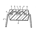
- the figure is a crosssectional view of a semiconductor device according to one embodiment of the present invention.
- a plate made of 99.99% aluminum, Al - 2%Si alloy or copper was subjected to electropolishing to form an experimental sample.
- This sample was a plate of 25mm x 20mm x 2mm.
- Such samples were each immersed in a solution of benzotriazole, tolyltriazole, sodium benzoate, azelaic acid, quinaldlic acid, rubeanic acid or cupferron in ethyl alcohol having various concentration at 40° C for 3 mintes, taken out and dried.
- a silicon chip 1 was mounted on a lead frame 2.
- a silver electrode 4 on the lead frame 2 was bonded to an aluminum electrode 5 on the silicon chip 1 with a copper wire 3.
- the resulting semiconductor device was immersed in a solution of benzotriazole in ethyl alcohol having a concentration of 0.16 M/l at 40° C for 3 minutes to form a metal-organic matter compound thereon.
- the treated semiconductor device was taken out of the solution and dried.
- An Ag-benzotriazole film 6 was formed on the surface of the silver electrode 4 of the lead frame 2 and a Cu-benzotriazole film 7 was formed on the surface of the copper wire 3, while an At -benzotriazole film 8 was formed on the surface of the aluminum electrode 5 of the silicon chip 1.
- the obtained semiconductor device was packaged with a molding resin 9.
Landscapes
- Structures Or Materials For Encapsulating Or Coating Semiconductor Devices Or Solid State Devices (AREA)
- Encapsulation Of And Coatings For Semiconductor Or Solid State Devices (AREA)
- Preventing Corrosion Or Incrustation Of Metals (AREA)
Applications Claiming Priority (2)
| Application Number | Priority Date | Filing Date | Title |
|---|---|---|---|
| JP128068/85 | 1985-06-14 | ||
| JP60128068A JPS61287155A (ja) | 1985-06-14 | 1985-06-14 | 半導体装置及び半導体装置の製造方法 |
Publications (3)
| Publication Number | Publication Date |
|---|---|
| EP0205190A2 true EP0205190A2 (fr) | 1986-12-17 |
| EP0205190A3 EP0205190A3 (en) | 1987-07-29 |
| EP0205190B1 EP0205190B1 (fr) | 1992-09-02 |
Family
ID=14975658
Family Applications (1)
| Application Number | Title | Priority Date | Filing Date |
|---|---|---|---|
| EP86108142A Expired - Lifetime EP0205190B1 (fr) | 1985-06-14 | 1986-06-13 | Procédé de fabrication d'un dispositif semi-conducteur encapsulé dans de la résine |
Country Status (5)
| Country | Link |
|---|---|
| US (1) | US4821148A (fr) |
| EP (1) | EP0205190B1 (fr) |
| JP (1) | JPS61287155A (fr) |
| KR (1) | KR900007303B1 (fr) |
| DE (1) | DE3686600T2 (fr) |
Cited By (6)
| Publication number | Priority date | Publication date | Assignee | Title |
|---|---|---|---|---|
| EP0792517A4 (fr) * | 1994-11-15 | 1998-06-24 | Formfactor Inc | Structures de contact electrique obtenues par configuration d'un fil souple |
| US6336269B1 (en) | 1993-11-16 | 2002-01-08 | Benjamin N. Eldridge | Method of fabricating an interconnection element |
| US6727579B1 (en) | 1994-11-16 | 2004-04-27 | Formfactor, Inc. | Electrical contact structures formed by configuring a flexible wire to have a springable shape and overcoating the wire with at least one layer of a resilient conductive material, methods of mounting the contact structures to electronic components, and applications for employing the contact structures |
| US6778406B2 (en) | 1993-11-16 | 2004-08-17 | Formfactor, Inc. | Resilient contact structures for interconnecting electronic devices |
| EP2444999A4 (fr) * | 2009-06-18 | 2012-11-14 | Rohm Co Ltd | Dispositif à semiconducteur |
| WO2015000592A1 (fr) * | 2013-07-03 | 2015-01-08 | Rosenberger Hochfrequenztechnik Gmbh & Co. Kg | Fils de connexion gainés pour boîtiers de matrice et procédés de fabrication de ces fils de connexion gainés |
Families Citing this family (74)
| Publication number | Priority date | Publication date | Assignee | Title |
|---|---|---|---|---|
| US5917707A (en) | 1993-11-16 | 1999-06-29 | Formfactor, Inc. | Flexible contact structure with an electrically conductive shell |
| US5476211A (en) * | 1993-11-16 | 1995-12-19 | Form Factor, Inc. | Method of manufacturing electrical contacts, using a sacrificial member |
| JPH02105418A (ja) * | 1988-10-14 | 1990-04-18 | Mitsubishi Electric Corp | 樹脂封止型半導体装置 |
| US5229646A (en) * | 1989-01-13 | 1993-07-20 | Mitsubishi Denki Kabushiki Kaisha | Semiconductor device with a copper wires ball bonded to aluminum electrodes |
| JPH0817189B2 (ja) * | 1989-01-13 | 1996-02-21 | 三菱電機株式会社 | 半導体装置の製造方法 |
| US5396104A (en) * | 1989-03-28 | 1995-03-07 | Nippon Steel Corporation | Resin coated bonding wire, method of manufacturing the same, and semiconductor device |
| US4916519A (en) * | 1989-05-30 | 1990-04-10 | International Business Machines Corporation | Semiconductor package |
| US5446620A (en) * | 1990-08-01 | 1995-08-29 | Staktek Corporation | Ultra high density integrated circuit packages |
| US5475920A (en) * | 1990-08-01 | 1995-12-19 | Burns; Carmen D. | Method of assembling ultra high density integrated circuit packages |
| US5377077A (en) * | 1990-08-01 | 1994-12-27 | Staktek Corporation | Ultra high density integrated circuit packages method and apparatus |
| WO1992003035A1 (fr) * | 1990-08-01 | 1992-02-20 | Staktek Corporation | Procede et appareil de production de boitiers de circuits integres de densite ultra-elevee |
| US5367766A (en) * | 1990-08-01 | 1994-11-29 | Staktek Corporation | Ultra high density integrated circuit packages method |
| US5448450A (en) * | 1991-08-15 | 1995-09-05 | Staktek Corporation | Lead-on-chip integrated circuit apparatus |
| US5316573A (en) * | 1992-03-12 | 1994-05-31 | International Business Machines Corporation | Corrosion inhibition with CU-BTA |
| US5310702A (en) * | 1992-03-20 | 1994-05-10 | Kulicke And Soffa Industries, Inc. | Method of preventing short-circuiting of bonding wires |
| US5702985A (en) * | 1992-06-26 | 1997-12-30 | Staktek Corporation | Hermetically sealed ceramic integrated circuit heat dissipating package fabrication method |
| US6205654B1 (en) * | 1992-12-11 | 2001-03-27 | Staktek Group L.P. | Method of manufacturing a surface mount package |
| US5484959A (en) * | 1992-12-11 | 1996-01-16 | Staktek Corporation | High density lead-on-package fabrication method and apparatus |
| US5801437A (en) * | 1993-03-29 | 1998-09-01 | Staktek Corporation | Three-dimensional warp-resistant integrated circuit module method and apparatus |
| US5644161A (en) * | 1993-03-29 | 1997-07-01 | Staktek Corporation | Ultra-high density warp-resistant memory module |
| US5369056A (en) * | 1993-03-29 | 1994-11-29 | Staktek Corporation | Warp-resistent ultra-thin integrated circuit package fabrication method |
| US7084656B1 (en) | 1993-11-16 | 2006-08-01 | Formfactor, Inc. | Probe for semiconductor devices |
| US7200930B2 (en) * | 1994-11-15 | 2007-04-10 | Formfactor, Inc. | Probe for semiconductor devices |
| US5820014A (en) | 1993-11-16 | 1998-10-13 | Form Factor, Inc. | Solder preforms |
| US20020053734A1 (en) | 1993-11-16 | 2002-05-09 | Formfactor, Inc. | Probe card assembly and kit, and methods of making same |
| US7073254B2 (en) | 1993-11-16 | 2006-07-11 | Formfactor, Inc. | Method for mounting a plurality of spring contact elements |
| KR0165299B1 (ko) * | 1994-11-11 | 1999-03-20 | 김광호 | 다층 광 기록 디스크 |
| AU4160096A (en) * | 1994-11-15 | 1996-06-06 | Formfactor, Inc. | Probe card assembly and kit, and methods of using same |
| GB9425031D0 (en) * | 1994-12-09 | 1995-02-08 | Alpha Metals Ltd | Printed circuit board manufacture |
| GB9425030D0 (en) | 1994-12-09 | 1995-02-08 | Alpha Metals Ltd | Silver plating |
| US20100065963A1 (en) | 1995-05-26 | 2010-03-18 | Formfactor, Inc. | Method of wirebonding that utilizes a gas flow within a capillary from which a wire is played out |
| US6025642A (en) * | 1995-08-17 | 2000-02-15 | Staktek Corporation | Ultra high density integrated circuit packages |
| KR100215181B1 (ko) * | 1995-10-06 | 1999-08-16 | 포만 제프리 엘 | 도전성 은/증합체 복합체의 부식 및 용해 방지구조물 |
| US8033838B2 (en) | 1996-02-21 | 2011-10-11 | Formfactor, Inc. | Microelectronic contact structure |
| US5994152A (en) | 1996-02-21 | 1999-11-30 | Formfactor, Inc. | Fabricating interconnects and tips using sacrificial substrates |
| US6905587B2 (en) | 1996-03-22 | 2005-06-14 | Ronald Redline | Method for enhancing the solderability of a surface |
| US6544397B2 (en) | 1996-03-22 | 2003-04-08 | Ronald Redline | Method for enhancing the solderability of a surface |
| TW335526B (en) * | 1996-07-15 | 1998-07-01 | Matsushita Electron Co Ltd | A semiconductor and the manufacturing method |
| KR100202668B1 (ko) * | 1996-07-30 | 1999-07-01 | 구본준 | 크랙 방지를 위한 반도체 패키지와 그 제조방법 및 제조장치 |
| US5773132A (en) * | 1997-02-28 | 1998-06-30 | International Business Machines Corporation | Protecting copper dielectric interface from delamination |
| US5945732A (en) | 1997-03-12 | 1999-08-31 | Staktek Corporation | Apparatus and method of manufacturing a warp resistant thermally conductive integrated circuit package |
| US5976964A (en) * | 1997-04-22 | 1999-11-02 | Micron Technology, Inc. | Method of improving interconnect of semiconductor device by utilizing a flattened ball bond |
| US6600215B1 (en) | 1998-04-02 | 2003-07-29 | Micron Technology, Inc. | Method and apparatus for coupling a semiconductor die to die terminals |
| US6177726B1 (en) * | 1999-02-11 | 2001-01-23 | Philips Electronics North America Corporation | SiO2 wire bond insulation in semiconductor assemblies |
| USRE45842E1 (en) | 1999-02-17 | 2016-01-12 | Ronald Redline | Method for enhancing the solderability of a surface |
| JP3367458B2 (ja) * | 1999-03-30 | 2003-01-14 | 株式会社デンソー | 半導体装置の製造方法 |
| WO2000074131A1 (fr) * | 1999-05-31 | 2000-12-07 | Infineon Technologies A.G. | Procede d'assemblage d'un boitier de composant a semi-conducteur |
| US6207551B1 (en) * | 1999-08-24 | 2001-03-27 | Conexant Systems, Inc. | Method and apparatus using formic acid vapor as reducing agent for copper wirebonding |
| US6572387B2 (en) | 1999-09-24 | 2003-06-03 | Staktek Group, L.P. | Flexible circuit connector for stacked chip module |
| US20020113322A1 (en) * | 2000-06-12 | 2002-08-22 | Shinichi Terashima | Semiconductor device and method to produce the same |
| US6608763B1 (en) | 2000-09-15 | 2003-08-19 | Staktek Group L.P. | Stacking system and method |
| EP1215724B1 (fr) * | 2000-11-20 | 2012-10-31 | Texas Instruments Incorporated | Dispositif semi-conducteur lié par fil avec un couplage à capacité réduite |
| DE10108695A1 (de) * | 2001-02-23 | 2002-09-05 | Varta Geraetebatterie Gmbh | Galvanisches Element mit mindestens einer lithiuminterkalierenden Elektrode |
| US6462408B1 (en) | 2001-03-27 | 2002-10-08 | Staktek Group, L.P. | Contact member stacking system and method |
| US7132736B2 (en) * | 2001-10-31 | 2006-11-07 | Georgia Tech Research Corporation | Devices having compliant wafer-level packages with pillars and methods of fabrication |
| US6849806B2 (en) * | 2001-11-16 | 2005-02-01 | Texas Instruments Incorporated | Electrical apparatus having resistance to atmospheric effects and method of manufacture therefor |
| TWI287282B (en) * | 2002-03-14 | 2007-09-21 | Fairchild Kr Semiconductor Ltd | Semiconductor package having oxidation-free copper wire |
| US6866255B2 (en) * | 2002-04-12 | 2005-03-15 | Xerox Corporation | Sputtered spring films with low stress anisotropy |
| US6621141B1 (en) | 2002-07-22 | 2003-09-16 | Palo Alto Research Center Incorporated | Out-of-plane microcoil with ground-plane structure |
| US20040119172A1 (en) * | 2002-12-18 | 2004-06-24 | Downey Susan H. | Packaged IC using insulated wire |
| MY134318A (en) * | 2003-04-02 | 2007-12-31 | Freescale Semiconductor Inc | Integrated circuit die having a copper contact and method therefor |
| US6900525B2 (en) * | 2003-05-21 | 2005-05-31 | Kyocera America, Inc. | Semiconductor package having filler metal of gold/silver/copper alloy |
| US7015584B2 (en) * | 2003-07-08 | 2006-03-21 | Xerox Corporation | High force metal plated spring structure |
| US7105379B2 (en) * | 2004-04-28 | 2006-09-12 | Taiwan Semiconductor Manufacturing Co., Ltd. | Implementation of protection layer for bond pad protection |
| US7230440B2 (en) * | 2004-10-21 | 2007-06-12 | Palo Alto Research Center Incorporated | Curved spring structure with elongated section located under cantilevered section |
| US8330485B2 (en) * | 2004-10-21 | 2012-12-11 | Palo Alto Research Center Incorporated | Curved spring structure with downturned tip |
| KR101360732B1 (ko) | 2007-06-27 | 2014-02-07 | 엘지이노텍 주식회사 | 발광 다이오드 패키지 |
| US20130277825A1 (en) * | 2012-04-18 | 2013-10-24 | Texas Instruments Incorporated | Method for Preventing Corrosion of Copper-Aluminum Intermetallic Compounds |
| CN105075023B (zh) * | 2013-02-18 | 2017-08-29 | 株式会社自动网络技术研究所 | 电连接结构和端子 |
| DE102015108736A1 (de) * | 2015-06-02 | 2016-12-08 | Osram Opto Semiconductors Gmbh | Optoelektronisches Bauelement und Verfahren zur Herstellung eines optoelektronischen Bauelements |
| JP2018037639A (ja) * | 2016-08-31 | 2018-03-08 | 株式会社東芝 | 半導体パッケージ、及び半導体パッケージの製造方法 |
| JP2020521878A (ja) * | 2017-05-26 | 2020-07-27 | ユニバーシティー・オブ・ノース・テキサス | Cuワイヤでボンディングしたデバイス組立におけるAlボンドパッドの腐食の機構的検討及び防止 |
| DE112020001490T5 (de) * | 2019-03-27 | 2021-12-30 | Sumitomo Bakelite Co., Ltd. | Harzzusammensetzung zum einkapseln und halbleitervorrichtung |
| TWI784272B (zh) * | 2019-05-31 | 2022-11-21 | 美商羅門哈斯電子材料有限公司 | 抗蝕劑組成物、其製造方法及包含其的製品 |
Family Cites Families (16)
| Publication number | Priority date | Publication date | Assignee | Title |
|---|---|---|---|---|
| JPS5038157B2 (fr) * | 1972-11-28 | 1975-12-08 | ||
| JPS50110279A (fr) * | 1974-02-06 | 1975-08-30 | ||
| US4248920A (en) * | 1978-04-26 | 1981-02-03 | Tokyo Shibaura Denki Kabushiki Kaisha | Resin-sealed semiconductor device |
| JPS5923009B2 (ja) * | 1979-06-26 | 1984-05-30 | 日本ビクター株式会社 | 磁気記録媒体 |
| US4327369A (en) * | 1979-08-06 | 1982-04-27 | Hi-Tech Industries, Inc. | Encapsulating moisture-proof coating |
| US4572853A (en) * | 1980-06-05 | 1986-02-25 | Tokyo Shibaura Denki Kabushiki Kaisha | Resin encapsulation type semiconductor device |
| JPS5769767A (en) * | 1980-10-20 | 1982-04-28 | Toshiba Corp | Resin sealed type semiconductor device |
| US4480009A (en) * | 1980-12-15 | 1984-10-30 | M&T Chemicals Inc. | Siloxane-containing polymers |
| US4486945A (en) * | 1981-04-21 | 1984-12-11 | Seiichiro Aigoo | Method of manufacturing semiconductor device with plated bump |
| US4373656A (en) * | 1981-07-17 | 1983-02-15 | Western Electric Company, Inc. | Method of preserving the solderability of copper |
| US4415629A (en) * | 1982-03-22 | 1983-11-15 | Electric Power Research Institute, Inc. | Insulated conductor |
| JPS58163652A (ja) * | 1982-03-25 | 1983-09-28 | トーレ・シリコーン株式会社 | 連続的な異相構造を有するシリコ−ン1体成形物,およびその製造方法 |
| JPS58166747A (ja) * | 1982-03-29 | 1983-10-01 | Toshiba Corp | 樹脂封止型半導体装置 |
| DE3278980D1 (en) * | 1982-04-30 | 1988-10-06 | Matsushita Electric Industrial Co Ltd | Magnetic recording medium |
| JPS58202556A (ja) * | 1982-05-21 | 1983-11-25 | Hitachi Ltd | 半導体装置 |
| JPS602681A (ja) * | 1983-06-16 | 1985-01-08 | Murata Mfg Co Ltd | 銅または銅合金の防錆処理方法 |
-
1985
- 1985-06-14 JP JP60128068A patent/JPS61287155A/ja active Granted
-
1986
- 1986-06-04 US US06/870,399 patent/US4821148A/en not_active Expired - Lifetime
- 1986-06-10 KR KR1019860004578A patent/KR900007303B1/ko not_active Expired
- 1986-06-13 EP EP86108142A patent/EP0205190B1/fr not_active Expired - Lifetime
- 1986-06-13 DE DE8686108142T patent/DE3686600T2/de not_active Expired - Fee Related
Cited By (11)
| Publication number | Priority date | Publication date | Assignee | Title |
|---|---|---|---|---|
| US6336269B1 (en) | 1993-11-16 | 2002-01-08 | Benjamin N. Eldridge | Method of fabricating an interconnection element |
| US6778406B2 (en) | 1993-11-16 | 2004-08-17 | Formfactor, Inc. | Resilient contact structures for interconnecting electronic devices |
| US6835898B2 (en) | 1993-11-16 | 2004-12-28 | Formfactor, Inc. | Electrical contact structures formed by configuring a flexible wire to have a springable shape and overcoating the wire with at least one layer of a resilient conductive material, methods of mounting the contact structures to electronic components, and applications for employing the contact structures |
| US7225538B2 (en) | 1993-11-16 | 2007-06-05 | Formfactor, Inc. | Resilient contact structures formed and then attached to a substrate |
| EP0792517A4 (fr) * | 1994-11-15 | 1998-06-24 | Formfactor Inc | Structures de contact electrique obtenues par configuration d'un fil souple |
| US6727579B1 (en) | 1994-11-16 | 2004-04-27 | Formfactor, Inc. | Electrical contact structures formed by configuring a flexible wire to have a springable shape and overcoating the wire with at least one layer of a resilient conductive material, methods of mounting the contact structures to electronic components, and applications for employing the contact structures |
| EP2444999A4 (fr) * | 2009-06-18 | 2012-11-14 | Rohm Co Ltd | Dispositif à semiconducteur |
| US9780069B2 (en) | 2009-06-18 | 2017-10-03 | Rohm Co., Ltd. | Semiconductor device |
| US10163850B2 (en) | 2009-06-18 | 2018-12-25 | Rohm Co., Ltd. | Semiconductor device |
| WO2015000592A1 (fr) * | 2013-07-03 | 2015-01-08 | Rosenberger Hochfrequenztechnik Gmbh & Co. Kg | Fils de connexion gainés pour boîtiers de matrice et procédés de fabrication de ces fils de connexion gainés |
| US9997489B2 (en) | 2013-07-03 | 2018-06-12 | Rosenberger Hochfrequenztechnik Gmbh & Co. Kg | Coated bond wires for die packages and methods of manufacturing said coated bond wires |
Also Published As
| Publication number | Publication date |
|---|---|
| KR900007303B1 (ko) | 1990-10-08 |
| DE3686600T2 (de) | 1993-04-15 |
| KR870000752A (ko) | 1987-02-20 |
| EP0205190A3 (en) | 1987-07-29 |
| JPS61287155A (ja) | 1986-12-17 |
| EP0205190B1 (fr) | 1992-09-02 |
| US4821148A (en) | 1989-04-11 |
| JPH045267B2 (fr) | 1992-01-30 |
| DE3686600D1 (de) | 1992-10-08 |
Similar Documents
| Publication | Publication Date | Title |
|---|---|---|
| US4821148A (en) | Resin packaged semiconductor device having a protective layer made of a metal-organic matter compound | |
| EP0273294B1 (fr) | Procédé pour éliminer des époxydes réticulés | |
| CA1172525A (fr) | Revetement anti-corrosion pour articles contenant du cuivre et methode de preparation | |
| EP0357219A1 (fr) | Aluminium et alliage d'aluminium ayant une couche protectrice résistant à la corrosion et procédés pour la fabrication d'une telle couche | |
| WO2004090941A2 (fr) | Puce de circuit integre presentant un contact en cuivre et procede associe | |
| KR20020040788A (ko) | 구리 기판의 선택적 침착방법 | |
| EP0083631A1 (fr) | Procede permettant de conserver les caracteristiques de soudage du cuivre. | |
| CN101840846A (zh) | 半导体封装的金属部分上的金属可焊性保持涂层 | |
| JP5306646B2 (ja) | 錫表面の耐食性の向上 | |
| EP3427297A1 (fr) | Structure de grille de connexion, grille de connexion, dispositif électronique à montage en surface et leurs procédés de production | |
| US3831066A (en) | Hermetically sealed semiconductor device with corrosion inhibited ferrous metal portions | |
| JPS6310547A (ja) | 半導体装置 | |
| KR20200012910A (ko) | 본딩 표면상의 구리 표면을 위한 부식 억제제 층 및 부식 억제제 층을 사용하여 와이어 본딩에 제공된 구리 표면을 보호하기 위한 방법 | |
| KR100271558B1 (ko) | 구리계 리드프레임의 수지누출억제 및 표면부식방지용 조성물 | |
| JPH0478173B2 (fr) | ||
| JPH11286794A (ja) | 銅または銅合金材料の表面処理方法 | |
| JPS63291443A (ja) | 半導体装置の製造方法 | |
| JPS5847853B2 (ja) | デンシブヒンドウタイノボウシヨクホウホウ | |
| JPH1161458A (ja) | 銅合金リードフレームの表面処理剤 | |
| JPH046101B2 (fr) | ||
| US6165278A (en) | Removing thermal grease from electronic cards | |
| Bhide | Decapsulation of silicone-epoxy copolymer packages | |
| Kumar | Corrosion of the joining metallurgy in multilayer substrates during processing | |
| JPS6038849A (ja) | 半導体装置およびその製造方法 | |
| KR20070030845A (ko) | 주석 표면의 내부식성 증강 방법 |
Legal Events
| Date | Code | Title | Description |
|---|---|---|---|
| PUAI | Public reference made under article 153(3) epc to a published international application that has entered the european phase |
Free format text: ORIGINAL CODE: 0009012 |
|
| AK | Designated contracting states |
Kind code of ref document: A2 Designated state(s): DE GB |
|
| PUAL | Search report despatched |
Free format text: ORIGINAL CODE: 0009013 |
|
| AK | Designated contracting states |
Kind code of ref document: A3 Designated state(s): DE GB |
|
| 17P | Request for examination filed |
Effective date: 19870731 |
|
| 17Q | First examination report despatched |
Effective date: 19900808 |
|
| GRAA | (expected) grant |
Free format text: ORIGINAL CODE: 0009210 |
|
| AK | Designated contracting states |
Kind code of ref document: B1 Designated state(s): DE GB |
|
| REF | Corresponds to: |
Ref document number: 3686600 Country of ref document: DE Date of ref document: 19921008 |
|
| PGFP | Annual fee paid to national office [announced via postgrant information from national office to epo] |
Ref country code: GB Payment date: 19930603 Year of fee payment: 8 |
|
| PLBE | No opposition filed within time limit |
Free format text: ORIGINAL CODE: 0009261 |
|
| STAA | Information on the status of an ep patent application or granted ep patent |
Free format text: STATUS: NO OPPOSITION FILED WITHIN TIME LIMIT |
|
| 26N | No opposition filed | ||
| PG25 | Lapsed in a contracting state [announced via postgrant information from national office to epo] |
Ref country code: GB Effective date: 19940613 |
|
| GBPC | Gb: european patent ceased through non-payment of renewal fee |
Effective date: 19940613 |
|
| PGFP | Annual fee paid to national office [announced via postgrant information from national office to epo] |
Ref country code: DE Payment date: 19970630 Year of fee payment: 12 |
|
| PG25 | Lapsed in a contracting state [announced via postgrant information from national office to epo] |
Ref country code: DE Free format text: LAPSE BECAUSE OF NON-PAYMENT OF DUE FEES Effective date: 19990401 |