EP0205274A2 - Système numérique de commande automatique de vol - Google Patents
Système numérique de commande automatique de vol Download PDFInfo
- Publication number
- EP0205274A2 EP0205274A2 EP86303985A EP86303985A EP0205274A2 EP 0205274 A2 EP0205274 A2 EP 0205274A2 EP 86303985 A EP86303985 A EP 86303985A EP 86303985 A EP86303985 A EP 86303985A EP 0205274 A2 EP0205274 A2 EP 0205274A2
- Authority
- EP
- European Patent Office
- Prior art keywords
- data
- processor
- independent
- data storage
- storage element
- Prior art date
- Legal status (The legal status is an assumption and is not a legal conclusion. Google has not performed a legal analysis and makes no representation as to the accuracy of the status listed.)
- Granted
Links
Images

Classifications
-
- G—PHYSICS
- G06—COMPUTING OR CALCULATING; COUNTING
- G06F—ELECTRIC DIGITAL DATA PROCESSING
- G06F11/00—Error detection; Error correction; Monitoring
- G06F11/07—Responding to the occurrence of a fault, e.g. fault tolerance
- G06F11/16—Error detection or correction of the data by redundancy in hardware
-
- G—PHYSICS
- G05—CONTROLLING; REGULATING
- G05D—SYSTEMS FOR CONTROLLING OR REGULATING NON-ELECTRIC VARIABLES
- G05D1/00—Control of position, course, altitude or attitude of land, water, air or space vehicles, e.g. using automatic pilots
- G05D1/0055—Control of position, course, altitude or attitude of land, water, air or space vehicles, e.g. using automatic pilots with safety arrangements
- G05D1/0077—Control of position, course, altitude or attitude of land, water, air or space vehicles, e.g. using automatic pilots with safety arrangements using redundant signals or controls
-
- G—PHYSICS
- G06—COMPUTING OR CALCULATING; COUNTING
- G06F—ELECTRIC DIGITAL DATA PROCESSING
- G06F11/00—Error detection; Error correction; Monitoring
- G06F11/07—Responding to the occurrence of a fault, e.g. fault tolerance
- G06F11/16—Error detection or correction of the data by redundancy in hardware
- G06F11/1629—Error detection by comparing the output of redundant processing systems
Definitions
- the invention relates to digital automatic flight control systems, particularly with respect to data management apparatus therefor.
- Present day digital automatic flight control system channels traditionally utilise dual digital processors responsive to the same or similar data with cross-processor monitoring for detecting random failures or generic design errors in the channels, thereby providing fail passive performance.
- the dual processors may be identical with respect to each other in hardware and software performing identical tasks. Alternatively, the processors may provide dissimilar data processing with respect to each other while performing identical tasks. In this arrangement, the processors may be dissimilar with respect to hardware, with respect to software or with respect to both hardware and software.
- a further dual processor fail passive arrangement is disclosed in co-pending European Patent Application No. 86303800.6. In co-pending Application No. 86303800.6 the dual processors are similar with respect to each other in hardware and software, but perform disparate tasks over disjoint computation paths with respect to each other.
- One of the processors performs an automatic flight control system function, while the other processor executes a monitor for that function to determine if the aircraft is performing in a manner prohibited by the function.
- the two processors may have access to a single data sensor set traditionally including a plurality of sensor subsystems to provide input information to the processors for controlling the aircraft.
- Each subsystem provides a plurality of data items formatted as a sequence of words or bytes. Typically a byte may comprise eight bits.
- One such subsystem comprises the air data computer subsystem which provides data with respect to Mach, airspeed, dynamic pressure, vertical speed and the like.
- Another such subsystem is the attitude and heading reference system (AHRS) which provides such data as roll and pitch attitude, heading, accelerations and body rates utilised, for example, to stabilise the inner loops of the automatic flight control system.
- Another such input data subsystem is the navigation subsystem providing such data as present position, velocity, acceleration and the like. The output from each subsystem containing the sequence of bytes therefrom may be considered as a data message from the subsystem.
- a single, bit-serial data bus to convey the data messages from the sensor subsystems to the processors.
- the single bus architecture is simpler in hardware configuration, less bulky, less expensive and more light weight than, for example, a parallel bus architecture, which qualities are significant for efficacious utilisation in present day aircraft.
- a single, bit-serial data bus system a large amount of data is transferred between the sensor subsystems and the processor inputs during each iteration of the flight control program. Since the data transfer is bit-serial, the data rates utilised are extraordinarily high.
- one of the dual processors controls the bus timing and accepts all of the data utilising such well known techniques as direct memory accessing, program interrupts or sensor polling.
- the data acquiring processor utilises the data in the programs stored therein and also provides the data to the second processor for the redundant or dissimilar processing in the cross-processor monitoring arrangement to detect random faults and generic design errors as discussed above.
- the data receiving processor may corrupt the input data, utilise the corrupted data in its own processing and send the corrupted data to the other processor for cross-processor monitoring purposes. Since the data utilised by . both processors is identical, although erroneous, the cross-processor monitoring may detect the same although incorrect outputs from both processors, thereby not detecting that an error has occurred. Under such circumstances, dangerous data may propagate to the control surface servos to precipitate a hazardous situation.
- Another prior art arrangement utilising two processors which require the same data is the provision of a buffer to hold the data such that both processors have access thereto when required.
- Such an arrangement is utilised when inputting analogue data via an analogue-to-digital converter associated with each processor.
- Such an arrangement is not utilised with digital data and is completely impractical with the high speed, bit-serial data transfer described above.
- the present invention is defined in the appended claims and the objective thereof is to provide data integrity to multiple processors configured in a cross-processor performance assessment arrangement for hazard protection.
- This objective is achieved by data management apparatus for an automatic flight control system which includes at least two digital data processors which require data from the aircraft sensor complement.
- the data is transmitted, via a bus, from the sensors for storage in one of the processors where the bus is controlled by that processor.
- the data is simultaneously entered into an independent data storage unit which is addressed by an independent data storage sequencer that is synchronised by the data receiving processor.
- the other processor accesses the independent data storage element for receiving the data stored therein for storage and utilisation within the other processor.
- the apparatus is constructed and arranged such that the data receiving processor cannot write into the independent data storage element so that the data receiving processor cannot corrupt or destroy data stored therein.
- the invention may be utilised in an automatic flight control system of the type described in the co-pending European patent application referred to above and which is incorporated herein by reference in its entirety.
- the automatic flight control system includes an A-processor 10 and a B-processor 11 utilised within the system in a manner similar to that described in said co-pending European patent application.
- the processors 10 and 11 are preferably identical and of conventional architecture, and are of the general purpose, medium scale design, a variety of which are commercially procurable, and may be used in specifically constructed computers for airborne analysis and control for automatic flight control and flight director applications.
- an FZ-800 digital flight control computer commercially procurable from the Avionics Division of the Aerospace and Marine Group of the Sperry Corporation may be utiised in implementing the system.
- the FZ-800 computer is based on the Zylog Z-8002 microprocessor. Details with respect to the internal arrangement of the digital processors 10 and 11 and program stored therein are described in said co-pending European patent application.
- each of the processors 10 and 11 perform active automatic flight control system functions as well as monitoring functions therefor in the manner described therein. These active and monitoring functions are performed in response to data provided from plural sensor subsystems of the type described above where each subsystem provides a sequence of words or bytes conveying information with respect to the plurality of parameters that the sensors of the subsystem are measuring.
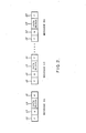
- each message consists of a start flag 12 identifying the start of the message followed by an address 13 identifying the sensor subsystem source of the data.
- a data field 14, following the address 13, comprises a sequence of bytes conveying the information with respect to the respective sensors of the subsystem. Each byte, for example, may comprise eight bits.
- the data field 14 is of variable length dependent on the number of bytes contained therein.
- An ending flag 15 follows the data block 14 identifying the end of the message.
- the system in which the present invention is included utilises a single, bit-serial data bus to which all of the sensor subsystems S1, S2, Vietnamese, SN are connected.
- Each of the messages illustrated in Figure 2 are placed on the bus by the associated subsystem in bit serial fashion with the messages S1, S2,...., SN being transmitted sequentially.
- serial data bus 20 receives the bit serial data from the sensor subsystems of the aircraft as described above with respect to Figure 2.
- the bus 20 is a high speed serial bus for conveying a large amount of information from the plural sensor subsystems to the processors 10 and 11 of the automatic flight control system during each iteration of the flight control programs.
- An active bus frame or cycle is utilised during which all of the sensor subsystems transfer their data messages via the bus 20 to the processors 10 and 11 in a manner to be described.
- the bit serial data on the bus 20 is buffered by a receiver 21 which applies the bit serial data to a serial-to-parallel converter 22.
- the serial-to-parallel converter 22 asembles the bit serial data on the bus 20 into words of bytes, of for example, eight bits each, representative of the data words provided by the sensors of the sensor subsystems.
- the converter 22 issues a data available signal to the A-processor 10 on a bus 23.
- the serial-to-parallel converter 22 is commanded by the processor 10 to place the assembled byte on a parallel data bus 24 in response to a read command signal issued by the processor 10 to the converter 22 on a bus 25.
- the converter 22 latches the assembled byte onto its output where it is sampled by the processor 10 via the bus 24.
- the A-processor 10 controls the timing of the serial bus 20 and the acquisition of the data from the sensor subsystems during the active bus frame. During this time, the A-processor 10 suspends its normal processing routines and dedicates its control fully to receiving the high speed bytes sequentially provided by the converter 22. During the active bus cycle when the A-processor 10 is receiving the data from the serial-to-parallel converter 22, the B-processor 11 is performing its normal processing routines since the processor 11 does not interface with the input bus 20. As the A-processor 10 receives the data on the bus 24, the processor 10 sequentially stores the data in an A-data storage element 26 associated therewith.
- This sequence of the data available signal issued by the converter 22 to the processor 10 on the bus 23 and the read command signal issued by the processor 10 to the converter 22 on the bus 25 results in the- processor 10 acquiring a byte of data and storing this byte in its data storage element 26. This process continues at a rapid rate during the active bus frame until all of the messages from the sensor. subsystems have been acquired by the processor 10 and stored in the data storage element 26 for later usage during the flight control program iteration.
- the processor 10 identifies the sensor subsystem from which a message is being received via the subsystem address 13 discussed above with respect to Figure 2.
- the A-processor 10 determines when the active bus frame is completed by identifying the address within the data message from the last subsystem to transmit, identified as subsystem N in Figure 2.
- the serial-to-parallel converter 22 provides the sensor data via the bus 24 to the processor 10 which stores the data in predetermined areas of its data storage element 26 in accordance with the respective sensor subsystem addresses. Simultaneously and independently, the serial-to-parallel converter 22 provides the data bytes to an independent data storage element 27 via a data path 28 that is independent of the processor 10. After the active bus frame is completed and all sensor subsystems have transferred their respective data to the independent data storage element 27, the B-Processor 11 can thereafter access the data storage element 27 and transfer all the data stored therein into a data storage element 29 associated therewith for use during the iteration of the flight control program for performing control and monitoring functions.
- the independent data storage element 27 stores all of the data provided during a complete bus frame as it is being accessed and controlled by the A-processor 10 such that the B-processor 11 has independent access to the entire set of bus data after completion of the active bus frame.
- the data is stored in predetermined areas of the storage element 27 in accordance with the sensor subsystem providing the data. These areas are designated as S1, S2, etc, SN corresponding to the respective sensor subsystems.
- This subsystem addressing is controlled by the A-processor 10 via a subsystem identifier address provided to the storage element 27 on an address bus 30.
- the addresses on the bus 30 are derived from the address field 13 of the respective subsystem message illustrated in Figure 2.
- the subsystem identifier address on the bus 30 controls the addressing of the data blocks arriving from the sensor subsystems as they sequentially are provided to the data storage element 27 via the parallel data bus 28.
- the subsystem identifier address provides the initial addresses for the areas of the storage element 27 determining where the blocks of data from the subsystems will reside in the storage element 27, respectively.
- the data is received it is stored in the data storage element 27 in a specific order such that when the B-processor 11 reads the data it has information with respect to the specific subsystems from which the respective sets of data are received.
- the processor 10 As the A-processor 10 receives each byte of data from the serial-to-parallel converter 22, the processor 10 provides a write command to the storage element 27 via a bus 31 to strobe the byte into the storage element 27 within the area controlled by the subsystem identifier address on the bus 30 at a location determined in a manner to be described.
- the A-processor 10 provides the starting address via the address bus 30 for entering a message from a sensor subsystem into the appropriate section of the data storage element 27.
- the A-processor 10 also stores the same data message in a similar arrangement in its data storage element 26.
- the A-processor 10 internally determines the addresses of the locations within the data storage element 26 whereat the bytes of the message are to be stored. If the A-processor 10 were to utilise these addresses for determining the locations for the individual bytes within a subsystem section of the data storage element 27, the processor 10, due to a fault or an error might scramble these addresses so as to place erroneous data in the memory locations.
- This erroneous data would then be utilised both by the A-processor 10 via its data storage element 26 and the B-processor 11 via its data storage element 29 after receiving the scrambled data from the independent data storage element 27. Since the same scrambled data would be utilised by both processors, the error may not be detected by the redundancy or monitoring techniques incorporated in the system. - Such data scrambling would have the same effect as corruption of the data by the A-processor 10 and then transmitting the corrupted data to the B-processor 11 for use in redundancy or monitoring processes.
- an independent data storage sequencer 32 is utilised in providing the addresses, via a data addressing bus 33, within the data blocks S1, S2, ....SN of the data storage element 27 for entering the bytes of the sensor subsystem messages.
- the independent data storage sequencer 32 provides a sequence of addresses independently of the A-processor 10. For each data message from a sensor subsystem, the independent data storage sequencer 32 is initially cleared to zero by an address clear signal issued by the A-processor 10 via a bus 34. As the bytes of the subsystem message are received from the serial-to-parallel converter 22, the address provided on the bus 33 by the independent data storage sequencer 32 is incremented sequentially for each byte of data received.
- the data in the storage element 26 is utilised for later processing during the flight control program iteration by the processor 10 and the data in the storage element 27 is thereafter transferred to the B-processor 11 for stoarge in its data storage element 29 for its processing during the flight control program iteration.
- the apparatus of the present invention is implemented in such a manner that the A-processor 10 cannot corrupt or destroy any data stored within the independent data storage element 27.
- the A-processor 10 cannot write into the data storage element 27.
- the data that is written into the storage. element 27 is provided directly via the independent data bus 28. Only the write command on the bus 31 and the subsystem identifier address on the address bus 30 is provided by the A-processor 10 to the independent data storage element 27.
- the data stored in the storage element 27 is transferred by the B-processor 11 into its data storage element 29 thereby releasing the data storage element 27 for the next active bus frame.
- the B-processor 11 addresses the storage element 27 with a sequence of read addresses via a read address bus 36 and issues corresponding read command signals on a bus 37 to the storage element 27 for sequentially providing the bytes stored in the storage element 27 to the B-processor 11 via a parallel data bus 38 for transfer to its data storage element 29.
- the processor 11 performs a block move of the entire data contents stored in the data storage element 27 to the data storage element 29 for use by the B-processor 11 during the flight control program iteration.
- the write addressing of the data storage element 27 for the individual data bytes within a subsystem data message is controlled by the independent data storage sequencer 32 such that the A-processor 10 cannot scramble this data within the data storage element 27.
- the addressing, however, for determining the area in the data storage element 27 for locating each of the subsystem data messages is performed by the A-processor 10 via the bus 30 and these location areas may be scrambled by the A-processor 10. If this occurs, both the processor 10 and the processor 11 may operate upon the same scrambled data, thereby possibly defeating the redundancy or monitoring procedures utilised and permitting the fault or error to remain undetected.
- the undetected scrambled data may precipitate a dangerous condition in the aircraft.
- the system is protected against this type of scrambling by utilising the source identifier address 13 ( Figure 2) within each of the data messages from the respective subsystems.
- the processor 11 verifies the source addresses to ensure that scrambling of subsystem data through a failure of the A-processor 10 has not occurred.
- each data source transmits within the data block 14 of Figure 2, a data checksum tracer and a new-data update validation tracer provided by a counter (not shown).
- These data tracers are utilised by both the A-processor 10 and the B-processor 11 to validate the data stored in the elements 26 and 27. This validation procedure protects against faults and/or design errors of the type which alter data bit patterns and/or inhibit data transfer through the single-string paths 20, 21, 22, 23 and 24.
- the messages illustrated in Figure 2 are sequentially transmitted in bit-serial fashion at high speed on the serial data bus 20.
- Each subsystem transmits its entire data message which is formatted into parallel bytes by the converter 22.
- the processor 10 utilises the address 13 ( Figure 2) to select the area within the storage element 27 at which to store the subsystem information.
- the processor 10 then clears the address in the independent data storage sequencer 32 via.the address clear signal on the bus 34.
- the bytes of the message are then received by the processor 10 and transferred to the data storage element 26.
- the processor 10 commands the bytes to be stored in the data storage element 27 via the write command on the bus 31 in the area determined by the address on the bus 30 at the locations determined by the addresses on the bus 33 from the independent data storage sequencer 32.
- the processor 10 commands the sequencer 32 sequentially to increment the address count such that the sequential bytes are stored at sequential locations in the appropriate area of the data storage element 27.
- the processor 10 recognises that an entire message has been received by detecting the ending flag 15 ( Figure 2).
- Processor 10 then prepares to receive the next subsystem data message by addressing the data storage element 27 via the subsystem identifier address bus 30 and clearing independent data storage sequencer 32 via the address clear signal on the bus 34.
- the processor 10 determines that all of the subsystem data messages have been received by identifying the address within the data message from subsystem SN.
- all of the subsystem data resides in the data storage element 26 and in successive areas within the data storage element 27.
- the data is transferred by the B-processor 11 from the data storage element 27 to the data storage element 29.
- the data storage element 27 is thereby released for use by the A-processor 10 in receiving the next sequential bus frame.
- the data then residing in the storage elements 26 and 29 are utilised by the processors 10 and 11, respectively, in performing active autopilot functions and monitoring processes as described in said co-pending European patent application or utilised in redundancy cross-processor monitoring for detecting faults and errors.
- data errors introduced into the data after transmission will be detected by at least one of the processors, which can then react to prevent potential resultant hazardous conditions in the automatic flight control system.
- a detected error or fault may result in various reversionary modes of the automatic flight control system such as disengaging a particular mode or possibly disengaging the entire automatic flight control system.
- the present invention provides independent distribution of serial data bus information to two redundant processing elements such that an error or fault within one processor cannot undetectibly corrupt or scramble the data utilised by more than one of the processors simultaneously. Such data integrity to multiple processors is necessary for implementation of a cross-processor performance assessment mode for hazard protection.
- the present invention protects the system against hazardous automatic flight control system malfunctions resulting from corruption or scrambling of the incoming primary data by one of plural redundant processors.
Landscapes
- Engineering & Computer Science (AREA)
- General Physics & Mathematics (AREA)
- Physics & Mathematics (AREA)
- Theoretical Computer Science (AREA)
- Remote Sensing (AREA)
- General Engineering & Computer Science (AREA)
- Aviation & Aerospace Engineering (AREA)
- Radar, Positioning & Navigation (AREA)
- Quality & Reliability (AREA)
- Automation & Control Theory (AREA)
- Debugging And Monitoring (AREA)
- Combined Controls Of Internal Combustion Engines (AREA)
- Multi Processors (AREA)
- Hardware Redundancy (AREA)
- Control Of Position, Course, Altitude, Or Attitude Of Moving Bodies (AREA)
- Management, Administration, Business Operations System, And Electronic Commerce (AREA)
- Control By Computers (AREA)
Applications Claiming Priority (2)
| Application Number | Priority Date | Filing Date | Title |
|---|---|---|---|
| US743535 | 1985-06-11 | ||
| US06/743,535 US4713757A (en) | 1985-06-11 | 1985-06-11 | Data management equipment for automatic flight control systems having plural digital processors |
Publications (3)
| Publication Number | Publication Date |
|---|---|
| EP0205274A2 true EP0205274A2 (fr) | 1986-12-17 |
| EP0205274A3 EP0205274A3 (en) | 1989-03-22 |
| EP0205274B1 EP0205274B1 (fr) | 1993-02-17 |
Family
ID=24989162
Family Applications (1)
| Application Number | Title | Priority Date | Filing Date |
|---|---|---|---|
| EP86303985A Expired - Lifetime EP0205274B1 (fr) | 1985-06-11 | 1986-05-27 | Système numérique de commande automatique de vol |
Country Status (8)
| Country | Link |
|---|---|
| US (1) | US4713757A (fr) |
| EP (1) | EP0205274B1 (fr) |
| JP (1) | JPS61285549A (fr) |
| BR (1) | BR8601026A (fr) |
| CA (1) | CA1244131A (fr) |
| DE (1) | DE3687765T2 (fr) |
| ES (1) | ES8800453A1 (fr) |
| IL (1) | IL78941A (fr) |
Cited By (2)
| Publication number | Priority date | Publication date | Assignee | Title |
|---|---|---|---|---|
| EP0742507A1 (fr) * | 1995-05-12 | 1996-11-13 | The Boeing Company | Procédé et dispositif de synchronisation d'ordinateurs de commande de vol |
| US8914551B2 (en) | 2013-04-09 | 2014-12-16 | Analog Devices, Inc. | Sensor polling unit for microprocessor integration |
Families Citing this family (14)
| Publication number | Priority date | Publication date | Assignee | Title |
|---|---|---|---|---|
| JPS61272877A (ja) * | 1985-05-28 | 1986-12-03 | Victor Co Of Japan Ltd | 画像生成装置 |
| AU1682188A (en) * | 1987-04-02 | 1988-11-02 | Stellar Computer Inc. | Dynamically assignable shared register sets |
| US5001646A (en) * | 1988-12-19 | 1991-03-19 | Mcdonnell Douglas Corporation | Automated helicopter flight control system |
| US5457800A (en) * | 1991-05-02 | 1995-10-10 | Smiths Industries Aerospace & Defense Systems, Inc. | Adaptable datalink interface |
| US6178476B1 (en) * | 1997-01-06 | 2001-01-23 | Texas Instruments Incorporated | Data communication interface including an integrated data processor and serial memory device |
| US6233640B1 (en) * | 1999-03-19 | 2001-05-15 | In-System Design, Inc. | Universal serial bus peripheral bridge with sequencer |
| DE10056198A1 (de) * | 2000-11-13 | 2002-02-14 | Infineon Technologies Ag | Kommunikationssystem zum Austausch von Daten unter Verwendung eines zusätzlichen Prozessors |
| US8315269B1 (en) | 2007-04-18 | 2012-11-20 | Cypress Semiconductor Corporation | Device, method, and protocol for data transfer between host device and device having storage interface |
| TWI448902B (zh) * | 2007-08-24 | 2014-08-11 | Cypress Semiconductor Corp | 具頁存取基礎處理器介面之橋接裝置 |
| US8090894B1 (en) | 2007-09-21 | 2012-01-03 | Cypress Semiconductor Corporation | Architectures for supporting communication and access between multiple host devices and one or more common functions |
| US7895387B1 (en) | 2007-09-27 | 2011-02-22 | Cypress Semiconductor Corporation | Devices and methods for sharing common target device with two different hosts according to common communication protocol |
| CN101881969B (zh) * | 2009-09-03 | 2012-03-14 | 中国航空无线电电子研究所 | 基于多任务并行处理的飞行管理系统及其方法 |
| JP2014059606A (ja) * | 2012-09-14 | 2014-04-03 | Yamaha Corp | 信号処理システムおよびプログラム |
| CN113165389A (zh) | 2018-12-03 | 2021-07-23 | 惠普发展公司,有限责任合伙企业 | 逻辑电路系统封装 |
Citations (2)
| Publication number | Priority date | Publication date | Assignee | Title |
|---|---|---|---|---|
| EP0044218A1 (fr) | 1980-07-15 | 1982-01-20 | Westinghouse Electric Corporation | Système de communication de données |
| EP0207611A2 (fr) | 1985-05-30 | 1987-01-07 | Honeywell Inc. | Système numérique de commande automatique de vol avec surveillance de fonctions dissemblables |
Family Cites Families (10)
| Publication number | Priority date | Publication date | Assignee | Title |
|---|---|---|---|---|
| NL285817A (fr) * | 1961-11-22 | |||
| US3699532A (en) * | 1970-04-21 | 1972-10-17 | Singer Co | Multiprogramming control for a data handling system |
| US3950729A (en) * | 1973-08-31 | 1976-04-13 | Nasa | Shared memory for a fault-tolerant computer |
| US3994456A (en) * | 1975-05-29 | 1976-11-30 | Sperry Rand Corporation | Steered lateral course transition control apparatus for aircraft area navigation systems |
| US4028668A (en) * | 1975-12-22 | 1977-06-07 | Honeywell Information Systems, Inc. | Apparatus for selectively addressing sections and locations in a device controller's memory |
| CA1118101A (fr) * | 1977-06-02 | 1982-02-09 | Jerry Doniger | Systeme digital de guidage en vol |
| US4156932A (en) * | 1977-07-05 | 1979-05-29 | Honeywell Information Systems Inc. | Programmable communications controller |
| US4270168A (en) * | 1978-08-31 | 1981-05-26 | United Technologies Corporation | Selective disablement in fail-operational, fail-safe multi-computer control system |
| FI801896A7 (fi) * | 1980-06-12 | 1981-01-01 | Kone Oy | Menetelmä ja laitteisto ulkopuolisten tulo- ja lähtötietojen välittämiseksi prosessorijärjestelmään. |
| JPS6053902B2 (ja) * | 1980-06-17 | 1985-11-27 | 三菱電機株式会社 | 電子計算機の並列システム |
-
1985
- 1985-06-11 US US06/743,535 patent/US4713757A/en not_active Expired - Lifetime
-
1986
- 1986-02-06 CA CA000501242A patent/CA1244131A/fr not_active Expired
- 1986-03-10 BR BR8601026A patent/BR8601026A/pt unknown
- 1986-05-27 DE DE8686303985T patent/DE3687765T2/de not_active Expired - Fee Related
- 1986-05-27 EP EP86303985A patent/EP0205274B1/fr not_active Expired - Lifetime
- 1986-05-27 JP JP61122034A patent/JPS61285549A/ja active Pending
- 1986-05-27 IL IL78941A patent/IL78941A/xx not_active IP Right Cessation
- 1986-06-10 ES ES555898A patent/ES8800453A1/es not_active Expired
Patent Citations (2)
| Publication number | Priority date | Publication date | Assignee | Title |
|---|---|---|---|---|
| EP0044218A1 (fr) | 1980-07-15 | 1982-01-20 | Westinghouse Electric Corporation | Système de communication de données |
| EP0207611A2 (fr) | 1985-05-30 | 1987-01-07 | Honeywell Inc. | Système numérique de commande automatique de vol avec surveillance de fonctions dissemblables |
Cited By (3)
| Publication number | Priority date | Publication date | Assignee | Title |
|---|---|---|---|---|
| EP0742507A1 (fr) * | 1995-05-12 | 1996-11-13 | The Boeing Company | Procédé et dispositif de synchronisation d'ordinateurs de commande de vol |
| US5790791A (en) * | 1995-05-12 | 1998-08-04 | The Boeing Company | Apparatus for synchronizing flight management computers where only the computer chosen to be the master received pilot inputs and transfers the inputs to the spare |
| US8914551B2 (en) | 2013-04-09 | 2014-12-16 | Analog Devices, Inc. | Sensor polling unit for microprocessor integration |
Also Published As
| Publication number | Publication date |
|---|---|
| ES8800453A1 (es) | 1987-10-16 |
| EP0205274B1 (fr) | 1993-02-17 |
| DE3687765D1 (de) | 1993-03-25 |
| IL78941A0 (en) | 1986-09-30 |
| US4713757A (en) | 1987-12-15 |
| JPS61285549A (ja) | 1986-12-16 |
| BR8601026A (pt) | 1987-01-13 |
| EP0205274A3 (en) | 1989-03-22 |
| IL78941A (en) | 1990-11-29 |
| CA1244131A (fr) | 1988-11-01 |
| ES555898A0 (es) | 1987-10-16 |
| DE3687765T2 (de) | 1993-06-24 |
Similar Documents
| Publication | Publication Date | Title |
|---|---|---|
| EP0205274B1 (fr) | Système numérique de commande automatique de vol | |
| Sklaroff | Redundancy management technique for space shuttle computers | |
| JPH0734179B2 (ja) | 複数の異種データ処理チヤンネルを有する自動飛行制御装置 | |
| US4115847A (en) | Automatic flight control system with operatively monitored digital computer | |
| JP2770976B2 (ja) | パリティ検査装置 | |
| US4354230A (en) | Synchronized, fail-operational, fail-safe multi-computer control system | |
| US3688099A (en) | Automatic control system with a digital computer | |
| US4634110A (en) | Fault detection and redundancy management system | |
| US4959768A (en) | Apparatus for tracking predetermined data for updating a secondary data base | |
| CA1118101A (fr) | Systeme digital de guidage en vol | |
| EP0278134A1 (fr) | Système de mémoire à disque à haute capacité avec un niveau et une bande de tolérance de fautes inhabituels | |
| US4317201A (en) | Error detecting and correcting RAM assembly | |
| US4280188A (en) | Survivable redundant vector sensors for systems with differing maximum output requirements | |
| US4231089A (en) | Data processing system with apparatus for correcting microinstruction errors | |
| US4942575A (en) | Error connection device for parity protected memory systems | |
| US5841969A (en) | Single bus architecture supporting subsystems of various criticality levels | |
| US3918309A (en) | Redundant inertial measurement system with improved failure-detection capability | |
| GB2237904A (en) | Digital control system | |
| JPS633351B2 (fr) | ||
| US5592680A (en) | Abnormal packet processing system | |
| JP2645021B2 (ja) | バス異常検査システム | |
| JPS60167547A (ja) | 信号伝送装置 | |
| Byrne et al. | Launch processing system | |
| JPH0335327A (ja) | 多数決障害処理装置 | |
| SKLAROFF et al. | Redundant system design for advanced digital flight control |
Legal Events
| Date | Code | Title | Description |
|---|---|---|---|
| PUAI | Public reference made under article 153(3) epc to a published international application that has entered the european phase |
Free format text: ORIGINAL CODE: 0009012 |
|
| AK | Designated contracting states |
Kind code of ref document: A2 Designated state(s): DE FR GB IT NL |
|
| RAP1 | Party data changed (applicant data changed or rights of an application transferred) |
Owner name: HONEYWELL INC. |
|
| PUAL | Search report despatched |
Free format text: ORIGINAL CODE: 0009013 |
|
| AK | Designated contracting states |
Kind code of ref document: A3 Designated state(s): DE FR GB IT NL |
|
| 17P | Request for examination filed |
Effective date: 19890906 |
|
| 17Q | First examination report despatched |
Effective date: 19910418 |
|
| GRAA | (expected) grant |
Free format text: ORIGINAL CODE: 0009210 |
|
| ITF | It: translation for a ep patent filed | ||
| AK | Designated contracting states |
Kind code of ref document: B1 Designated state(s): DE FR GB IT NL |
|
| REF | Corresponds to: |
Ref document number: 3687765 Country of ref document: DE Date of ref document: 19930325 |
|
| ET | Fr: translation filed | ||
| ITTA | It: last paid annual fee | ||
| PLBE | No opposition filed within time limit |
Free format text: ORIGINAL CODE: 0009261 |
|
| STAA | Information on the status of an ep patent application or granted ep patent |
Free format text: STATUS: NO OPPOSITION FILED WITHIN TIME LIMIT |
|
| 26N | No opposition filed | ||
| PGFP | Annual fee paid to national office [announced via postgrant information from national office to epo] |
Ref country code: FR Payment date: 19940314 Year of fee payment: 9 |
|
| PGFP | Annual fee paid to national office [announced via postgrant information from national office to epo] |
Ref country code: GB Payment date: 19940317 Year of fee payment: 9 |
|
| PGFP | Annual fee paid to national office [announced via postgrant information from national office to epo] |
Ref country code: DE Payment date: 19940319 Year of fee payment: 9 |
|
| PGFP | Annual fee paid to national office [announced via postgrant information from national office to epo] |
Ref country code: NL Payment date: 19940531 Year of fee payment: 9 |
|
| PG25 | Lapsed in a contracting state [announced via postgrant information from national office to epo] |
Ref country code: GB Effective date: 19950527 |
|
| PG25 | Lapsed in a contracting state [announced via postgrant information from national office to epo] |
Ref country code: NL Effective date: 19951201 |
|
| GBPC | Gb: european patent ceased through non-payment of renewal fee |
Effective date: 19950527 |
|
| NLV4 | Nl: lapsed or anulled due to non-payment of the annual fee |
Effective date: 19951201 |
|
| PG25 | Lapsed in a contracting state [announced via postgrant information from national office to epo] |
Ref country code: DE Effective date: 19960201 |
|
| PG25 | Lapsed in a contracting state [announced via postgrant information from national office to epo] |
Ref country code: FR Effective date: 19960229 |
|
| REG | Reference to a national code |
Ref country code: FR Ref legal event code: ST |
|
| REG | Reference to a national code |
Ref country code: FR Ref legal event code: ST |
|
| PG25 | Lapsed in a contracting state [announced via postgrant information from national office to epo] |
Ref country code: IT Free format text: LAPSE BECAUSE OF NON-PAYMENT OF DUE FEES;WARNING: LAPSES OF ITALIAN PATENTS WITH EFFECTIVE DATE BEFORE 2007 MAY HAVE OCCURRED AT ANY TIME BEFORE 2007. THE CORRECT EFFECTIVE DATE MAY BE DIFFERENT FROM THE ONE RECORDED. Effective date: 20050527 |