EP0205360B1 - Anschlussband für die Herstellung von elektrischen Bauelementen in Chipbauweise und Verfahren zur Herstellung dieser Bauelemente - Google Patents
Anschlussband für die Herstellung von elektrischen Bauelementen in Chipbauweise und Verfahren zur Herstellung dieser Bauelemente Download PDFInfo
- Publication number
- EP0205360B1 EP0205360B1 EP86400920A EP86400920A EP0205360B1 EP 0205360 B1 EP0205360 B1 EP 0205360B1 EP 86400920 A EP86400920 A EP 86400920A EP 86400920 A EP86400920 A EP 86400920A EP 0205360 B1 EP0205360 B1 EP 0205360B1
- Authority
- EP
- European Patent Office
- Prior art keywords
- component
- electrical
- connection belt
- fixing lugs
- connection
- Prior art date
- Legal status (The legal status is an assumption and is not a legal conclusion. Google has not performed a legal analysis and makes no representation as to the accuracy of the status listed.)
- Expired - Lifetime
Links
- 238000004519 manufacturing process Methods 0.000 title claims description 19
- 238000000034 method Methods 0.000 title claims description 10
- 239000011248 coating agent Substances 0.000 claims description 14
- 238000000576 coating method Methods 0.000 claims description 14
- 238000005520 cutting process Methods 0.000 claims description 11
- 238000000465 moulding Methods 0.000 claims description 8
- 229910052751 metal Inorganic materials 0.000 claims description 7
- 239000002184 metal Substances 0.000 claims description 7
- 238000012546 transfer Methods 0.000 claims description 7
- 238000005476 soldering Methods 0.000 claims description 6
- 238000002788 crimping Methods 0.000 claims description 4
- 238000003466 welding Methods 0.000 claims description 4
- 238000005452 bending Methods 0.000 claims description 3
- 239000011888 foil Substances 0.000 claims 6
- 239000003990 capacitor Substances 0.000 description 24
- 229920005989 resin Polymers 0.000 description 6
- 239000011347 resin Substances 0.000 description 6
- 239000000843 powder Substances 0.000 description 3
- 229910052782 aluminium Inorganic materials 0.000 description 2
- XAGFODPZIPBFFR-UHFFFAOYSA-N aluminium Chemical compound [Al] XAGFODPZIPBFFR-UHFFFAOYSA-N 0.000 description 2
- 230000015556 catabolic process Effects 0.000 description 2
- 238000006731 degradation reaction Methods 0.000 description 2
- 239000010408 film Substances 0.000 description 2
- 239000007788 liquid Substances 0.000 description 2
- 238000012423 maintenance Methods 0.000 description 2
- 239000000463 material Substances 0.000 description 2
- 239000011253 protective coating Substances 0.000 description 2
- 229920001342 Bakelite® Polymers 0.000 description 1
- 229910000906 Bronze Inorganic materials 0.000 description 1
- 239000004593 Epoxy Substances 0.000 description 1
- 229910000831 Steel Inorganic materials 0.000 description 1
- 240000008042 Zea mays Species 0.000 description 1
- 238000004026 adhesive bonding Methods 0.000 description 1
- 239000004637 bakelite Substances 0.000 description 1
- 239000011324 bead Substances 0.000 description 1
- 230000005540 biological transmission Effects 0.000 description 1
- 239000010974 bronze Substances 0.000 description 1
- 238000005266 casting Methods 0.000 description 1
- 230000001413 cellular effect Effects 0.000 description 1
- 230000003750 conditioning effect Effects 0.000 description 1
- 238000011109 contamination Methods 0.000 description 1
- KUNSUQLRTQLHQQ-UHFFFAOYSA-N copper tin Chemical compound [Cu].[Sn] KUNSUQLRTQLHQQ-UHFFFAOYSA-N 0.000 description 1
- 238000013461 design Methods 0.000 description 1
- 239000003989 dielectric material Substances 0.000 description 1
- XXBDWLFCJWSEKW-UHFFFAOYSA-N dimethylbenzylamine Chemical compound CN(C)CC1=CC=CC=C1 XXBDWLFCJWSEKW-UHFFFAOYSA-N 0.000 description 1
- 239000006260 foam Substances 0.000 description 1
- 239000011521 glass Substances 0.000 description 1
- 239000004615 ingredient Substances 0.000 description 1
- 238000001746 injection moulding Methods 0.000 description 1
- 238000009434 installation Methods 0.000 description 1
- 238000005259 measurement Methods 0.000 description 1
- 239000011104 metalized film Substances 0.000 description 1
- 239000011140 metalized polyester Substances 0.000 description 1
- SOOZEQGBHHIHEF-UHFFFAOYSA-N methyltetrahydrophthalic anhydride Chemical compound C1C=CCC2C(=O)OC(=O)C21C SOOZEQGBHHIHEF-UHFFFAOYSA-N 0.000 description 1
- 239000010445 mica Substances 0.000 description 1
- 229910052618 mica group Inorganic materials 0.000 description 1
- 238000003032 molecular docking Methods 0.000 description 1
- 238000004806 packaging method and process Methods 0.000 description 1
- 239000004033 plastic Substances 0.000 description 1
- 239000004848 polyfunctional curative Substances 0.000 description 1
- 238000007789 sealing Methods 0.000 description 1
- 238000000926 separation method Methods 0.000 description 1
- 229910000679 solder Inorganic materials 0.000 description 1
- 239000000243 solution Substances 0.000 description 1
- 239000010959 steel Substances 0.000 description 1
- 230000008646 thermal stress Effects 0.000 description 1
- 229910001174 tin-lead alloy Inorganic materials 0.000 description 1
- 210000002105 tongue Anatomy 0.000 description 1
- 238000001721 transfer moulding Methods 0.000 description 1
- 238000004804 winding Methods 0.000 description 1
Images



Classifications
-
- H—ELECTRICITY
- H01—ELECTRIC ELEMENTS
- H01G—CAPACITORS; CAPACITORS, RECTIFIERS, DETECTORS, SWITCHING DEVICES, LIGHT-SENSITIVE OR TEMPERATURE-SENSITIVE DEVICES OF THE ELECTROLYTIC TYPE
- H01G2/00—Details of capacitors not covered by a single one of groups H01G4/00-H01G11/00
- H01G2/02—Mountings
- H01G2/06—Mountings specially adapted for mounting on a printed-circuit support
- H01G2/065—Mountings specially adapted for mounting on a printed-circuit support for surface mounting, e.g. chip capacitors
-
- H—ELECTRICITY
- H01—ELECTRIC ELEMENTS
- H01G—CAPACITORS; CAPACITORS, RECTIFIERS, DETECTORS, SWITCHING DEVICES, LIGHT-SENSITIVE OR TEMPERATURE-SENSITIVE DEVICES OF THE ELECTROLYTIC TYPE
- H01G13/00—Apparatus specially adapted for manufacturing capacitors; Processes specially adapted for manufacturing capacitors not provided for in groups H01G4/00 - H01G11/00
- H01G13/006—Apparatus or processes for applying terminals
-
- Y—GENERAL TAGGING OF NEW TECHNOLOGICAL DEVELOPMENTS; GENERAL TAGGING OF CROSS-SECTIONAL TECHNOLOGIES SPANNING OVER SEVERAL SECTIONS OF THE IPC; TECHNICAL SUBJECTS COVERED BY FORMER USPC CROSS-REFERENCE ART COLLECTIONS [XRACs] AND DIGESTS
- Y10—TECHNICAL SUBJECTS COVERED BY FORMER USPC
- Y10T—TECHNICAL SUBJECTS COVERED BY FORMER US CLASSIFICATION
- Y10T29/00—Metal working
- Y10T29/43—Electric condenser making
- Y10T29/435—Solid dielectric type
-
- Y—GENERAL TAGGING OF NEW TECHNOLOGICAL DEVELOPMENTS; GENERAL TAGGING OF CROSS-SECTIONAL TECHNOLOGIES SPANNING OVER SEVERAL SECTIONS OF THE IPC; TECHNICAL SUBJECTS COVERED BY FORMER USPC CROSS-REFERENCE ART COLLECTIONS [XRACs] AND DIGESTS
- Y10—TECHNICAL SUBJECTS COVERED BY FORMER USPC
- Y10T—TECHNICAL SUBJECTS COVERED BY FORMER US CLASSIFICATION
- Y10T29/00—Metal working
- Y10T29/49—Method of mechanical manufacture
- Y10T29/49002—Electrical device making
- Y10T29/49117—Conductor or circuit manufacturing
- Y10T29/49169—Assembling electrical component directly to terminal or elongated conductor
- Y10T29/49171—Assembling electrical component directly to terminal or elongated conductor with encapsulating
- Y10T29/49172—Assembling electrical component directly to terminal or elongated conductor with encapsulating by molding of insulating material
-
- Y—GENERAL TAGGING OF NEW TECHNOLOGICAL DEVELOPMENTS; GENERAL TAGGING OF CROSS-SECTIONAL TECHNOLOGIES SPANNING OVER SEVERAL SECTIONS OF THE IPC; TECHNICAL SUBJECTS COVERED BY FORMER USPC CROSS-REFERENCE ART COLLECTIONS [XRACs] AND DIGESTS
- Y10—TECHNICAL SUBJECTS COVERED BY FORMER USPC
- Y10T—TECHNICAL SUBJECTS COVERED BY FORMER US CLASSIFICATION
- Y10T428/00—Stock material or miscellaneous articles
- Y10T428/12—All metal or with adjacent metals
- Y10T428/12188—All metal or with adjacent metals having marginal feature for indexing or weakened portion for severing
- Y10T428/12194—For severing perpendicular to longitudinal dimension
-
- Y—GENERAL TAGGING OF NEW TECHNOLOGICAL DEVELOPMENTS; GENERAL TAGGING OF CROSS-SECTIONAL TECHNOLOGIES SPANNING OVER SEVERAL SECTIONS OF THE IPC; TECHNICAL SUBJECTS COVERED BY FORMER USPC CROSS-REFERENCE ART COLLECTIONS [XRACs] AND DIGESTS
- Y10—TECHNICAL SUBJECTS COVERED BY FORMER USPC
- Y10T—TECHNICAL SUBJECTS COVERED BY FORMER US CLASSIFICATION
- Y10T428/00—Stock material or miscellaneous articles
- Y10T428/12—All metal or with adjacent metals
- Y10T428/12361—All metal or with adjacent metals having aperture or cut
- Y10T428/12368—Struck-out portion type
Definitions
- the present invention relates to a connection strip used in the manufacture of electrical components intended to be used with flat wave transfer.
- connection strip for such an electrical component in which at least one of the fixing lugs has a boss.
- capacitors made of metallized polyester for example, are degraded as a result of mechanical deformations due to the shrinkage of the films used, between the two non-shooped faces of the parallelepiped corresponding to the sawing faces of the mother capacitor.
- the connections of the capacitor are defined by electrical contacts constituted by U-shaped profiles comprising throttling zones so as to reduce the thermal conduction at the level of contact fingers while ensuring satisfactory electrical conduction.
- the use of contact fingers, between each lateral shooping of the parallelepiped and the external electrical connection of the finished capacitor reduces the thermal conduction between the capacitor itself and the exterior electrical connection. In this way, during the wave soldering step, the heat transmission is sufficiently low to cause no degradation of the capacitor itself.
- This capacitor involves two U-shaped profiles having contact fingers which are welded to the shoopings, the space between the profiles is then filled with resin and the assembly is cut to form individual capacitors.
- Patent application EP-A 0 130 001 describes a connection strip for the manufacture of an electric component with direct transfer.
- the strip is obtained from a metal sheet.
- the component consists of a passive element having two electrical terminations. The whole is embedded in a protective coating.
- the component must include two electrical connections, each of the connections has a part located on the surface of the coating to form one of the electrodes of the component and a part ensuring the electrical connection with the corresponding termination. Cutouts are made in the sheet to make the electrical connections.
- Two fixing lugs are intended to be folded over the electrical terminations to hold the element in position and ensure the electrical connection.
- the component electrodes are formed by cutting and bending.
- connection strip serving during the entire manufacturing cycle: firstly as a support for the elements which are welded on lugs integral with the strip.
- the strip then serves as a joint plane for molding the coating resin. Cutting the strip then makes the electrical connections to the component.
- the seal produced by the strip during molding makes it possible to avoid any risk of soiling on the final connections of the capacitor. Due to its general design, this strip allows easy and precise positioning of the parts and reliable docking, therefore greater reliability and better quality for the soldering of the components on the legs.
- connection strip has a boss at the minus one of the fixing lugs, the top of which provides the connection with the corresponding electrical termination.
- the fixing lugs can advantageously be obtained by an H-shaped cutout.
- at least one of the fixing lugs has a boss whose top ensures the connection with the corresponding electrical termination.
- FIG. 1 shows an electronic element intended to be packaged as a direct transfer component.
- the element 1 is for example a capacitor obtained by a stack 2 of metallized films.
- the electrical terminations 3 and 4 of the element 1 are constituted by "shooping" of two opposite faces of the parallelepiped constituting the element.
- FIG 2 is a top view of a connecting strip 5 allowing the conditioning of the element 1.
- the strip 5 consists of a flexible metal sheet 6 of material of low thermal conductivity (steel, bronze etc.).
- the metal of the sheet must be able to be welded on the "shoopages" 3 and 4.
- the material of these terminations is generally aluminum used alone or successive layers of aluminum and a tin-lead alloy. The sheet metal will be chosen accordingly.
- H-shaped cutouts were made to have two metal tabs 7 and 8 which will serve as fixing lugs.
- the cutting is carried out so that the attachment of the tabs to the rest of the sheet is carried out according to flared surfaces as shown in Figure 2. This will facilitate their folding and will give better elasticity to the fixing lugs to maintain the 'Element 1. Other cuts are made which will determine the electrodes of future components. These are the L-shaped cutouts as shown in FIG. 2 under the reference 9.
- Each H cut corresponds to four L cuts that frame it.
- Each lateral edge of the sheet is pierced with holes 10 which will be used for driving it by an appropriate device in the context of automated manufacturing.
- FIG. 3 is a detail view showing such an arrangement.
- the element 1 is placed upright but it could be laid flat. It is held in position by the lugs 7 and 8. It is advantageous to make certain adjustments to the fixing lugs for the following reasons.
- the tabs 7 and 8 will be provided with bosses 11 whose peaks will ensure electrical contact and mechanical maintenance with the element 1.
- it must be able to withstand without damage the thermal stresses of the postponement to dish.
- a reduction in section of the fixing lugs makes it possible to create a thermal resistance between the terminations of the element 1 and its electrodes.
- the section restriction is made over a short length so as not to increase the series resistance of the connection too much and consequently the losses of the capacitor.
- the restricted section can be obtained by holes 12 drilled in the fixing lugs.
- Other shapes can be envisaged, as shown by the fixing lugs 13 in FIG. 4, 14 in FIG. 5 and 15 in FIG. 6.
- the permanent connection of the tabs on the element can be obtained by welding.
- the connecting strip will advantageously serve as a joint plane for molding.
- the coating of the elements can be carried out according to various known techniques. It is possible, for example, to carry out a liquid injection molding of a self-extinguishing resin, a powder transfer molding, a casting, etc.
- One type of resin that can be used is that bearing the reference 0451 Bakelite, which has the advantage of ensuring good thermal protection of the component during wave soldering.
- Other ingredients include the MTHPA hardener and the BDMA accelerator.
- the resin can also be: uncharged with low thermal conductivity, charged (hollow glass beads, mica powder, etc.) or cellular in the form of foam.
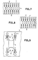
- Figures 7 and 8 are respectively top and bottom views of the conduction strip after coating of the elements. These figures have the advantage of showing the size of the coated element 16 with respect to the rest of the sheet 6. Thanks to FIG. 8, it can be seen how the tabs 7 and 8 come out of the coating.
- coated elements presented on a continuous or discontinuous strip, are ready for the last stages of the cutting manufacturing process: and folding of the electrodes.
- the clips are produced which will be used to hold the electrodes on their future locations. For this, a cut is made along the dotted lines referenced 17 in FIG. 9 and the parts 18 are folded at a right angle as indicated by the arrows. Note that it is possible to provide the cutouts 17 initially. We then proceed to the individual cutting of each capacitor. This cutting can be carried out along the dotted lines 19 as indicated in FIG. 9.
- FIG. 10 represents the component obtained after separation from the sheet 6.
- the shape of the electrodes 20 and 21 is a result of the cuts 9, 17 and 19 and of the previous folding operation.
- the electrodes 20 and 21 are then folded at right angles in the direction indicated by the arrows. They are then crimped onto the coating of the component as shown in Figure 11 for electrode 21.
- FIG. 12 represents the component obtained at the end of the operation. Note the housings 22 provided for crimping.
- the marking of the components can be carried out in a conventional manner or by laser inscription.
- the component can be packaged in bulk or on tape.
- the passive or active elements can be arranged flat or in the field.
- the fixing lugs can be arranged parallel to or at 90 ° to the electrodes. It is also possible to provide folds so as to place the element more stable before welding.
- FIG. 13 shows another possible configuration for the connecting strip. To facilitate understanding, several steps of the process have been shown in the same figure.
- the sheet 30 has first cutouts 31 intended to form, after folding, the fixing lugs 32 and 33. As previously, these lugs can have bosses 34 and holes 35. There are also two other folds 36 which will serve for positioning the element 37 laid flat.
- the sheet 30 also has second cutouts 38 alternating with the first ones.
- the parts 39 located between the first and second cuts will form after a new cut of the sheet and after folding the electrodes of the components.
- the limits of the coating have been shown in broken lines 40. After a cut along the dotted lines 41, the electrodes of the component are delimited.
- FIG. 14 represents yet another configuration for which the electrodes of the component are folded in planes parallel to the fixing lugs.
- the element 50 is held by the fixing lugs 51 and 52 obtained after cutting 53 and folding the lugs.
- These cutouts 53 are framed by other cutouts 54 made in the connection strip 55 which has not been shown in its entire width.
- the broken line 56 represents the limits of the coating.
- the dotted lines 57 represent the cutouts which will then occur.
Landscapes
- Engineering & Computer Science (AREA)
- Power Engineering (AREA)
- Microelectronics & Electronic Packaging (AREA)
- Manufacturing & Machinery (AREA)
- Fixed Capacitors And Capacitor Manufacturing Machines (AREA)
- Apparatuses And Processes For Manufacturing Resistors (AREA)
- Ceramic Capacitors (AREA)
Claims (9)
Applications Claiming Priority (2)
| Application Number | Priority Date | Filing Date | Title |
|---|---|---|---|
| FR8507148 | 1985-05-10 | ||
| FR8507148A FR2581827B1 (fr) | 1985-05-10 | 1985-05-10 | Bande de connexion pour la fabrication de composants electriques a report direct et procede de fabrication de ces composants |
Publications (2)
| Publication Number | Publication Date |
|---|---|
| EP0205360A1 EP0205360A1 (de) | 1986-12-17 |
| EP0205360B1 true EP0205360B1 (de) | 1990-01-03 |
Family
ID=9319171
Family Applications (1)
| Application Number | Title | Priority Date | Filing Date |
|---|---|---|---|
| EP86400920A Expired - Lifetime EP0205360B1 (de) | 1985-05-10 | 1986-04-25 | Anschlussband für die Herstellung von elektrischen Bauelementen in Chipbauweise und Verfahren zur Herstellung dieser Bauelemente |
Country Status (5)
| Country | Link |
|---|---|
| US (1) | US4715118A (de) |
| EP (1) | EP0205360B1 (de) |
| JP (1) | JPS6230306A (de) |
| DE (1) | DE3668091D1 (de) |
| FR (1) | FR2581827B1 (de) |
Families Citing this family (17)
| Publication number | Priority date | Publication date | Assignee | Title |
|---|---|---|---|---|
| US4934048A (en) * | 1985-06-07 | 1990-06-19 | American Precision Industries Inc. | Method of making surface mountable electronic device |
| JPS62245583A (ja) * | 1986-04-17 | 1987-10-26 | Fuji Photo Film Co Ltd | 磁気テ−プカセツト用パツドの製造方法 |
| FR2609207B1 (fr) * | 1986-12-30 | 1989-10-20 | Europ Composants Electron | Barrette de connexions pour la fabrication de composants electriques |
| US4819115A (en) * | 1988-01-28 | 1989-04-04 | Westinghouse Electric Corp. | End connections for wound capacitors and methods of making the same |
| FR2634414B1 (fr) * | 1988-07-22 | 1990-10-19 | Europ Composants Electron | Dispositif d'injection de matiere plastique liquide dans un moule, en particulier de matiere thermodurcissable pour l'enrobage de composants electroniques |
| DE3829934C1 (en) * | 1988-09-02 | 1990-02-22 | Roederstein Spezialfabriken Fuer Bauelemente Der Elektronik Und Kondensatoren Der Starkstromtechnik Gmbh, 8300 Landshut, De | Device for processing the plastic sheathing of electrical chip components on a carrier strip |
| FR2641905B1 (fr) * | 1988-12-23 | 1991-03-15 | Europ Composants Electron | Bande de connexions pour assemblage en ligne de composants cms |
| FR2645338B1 (fr) * | 1989-03-31 | 1991-06-07 | Composants Electro Lcc Cie Eur | Procede de fabrication d'anodes fil pour condensateurs electrolytiques et dispositif pour sa mise en oeuvre |
| US5263241A (en) * | 1992-04-06 | 1993-11-23 | Delco Electronics Corporation | Apparatus useful in the manufacture of a pressure sensor assembly |
| DE4446566A1 (de) * | 1994-12-24 | 1996-06-27 | Telefunken Microelectron | Mehrpoliges, oberflächenmontierbares, elektronisches Bauelement |
| US5939955A (en) * | 1997-06-10 | 1999-08-17 | Bel Fuse, Inc. | Assembly of inductors wound on bobbin of encapsulated electrical components |
| JP3412521B2 (ja) * | 1998-07-10 | 2003-06-03 | 株式会社村田製作所 | 電子部品 |
| EP1011117A3 (de) | 1998-12-15 | 2004-11-10 | Murata Manufacturing Co., Ltd. | Monolithischer keramischer kondensator |
| US6924967B1 (en) * | 2004-04-30 | 2005-08-02 | Alan Devoe | Noninterdigitated mounting for interdigitated stacked capacitor and method |
| US7419084B2 (en) * | 2004-11-24 | 2008-09-02 | Xerox Corporation | Mounting method for surface-mount components on a printed circuit board |
| US7898818B2 (en) * | 2007-03-07 | 2011-03-01 | Dell Products, Lp | Variably orientated capacitive elements for printed circuit boards and method of manufacturing same |
| KR102142516B1 (ko) * | 2018-09-04 | 2020-08-07 | 삼성전기주식회사 | 전자 부품 |
Family Cites Families (5)
| Publication number | Priority date | Publication date | Assignee | Title |
|---|---|---|---|---|
| US4158218A (en) * | 1977-09-19 | 1979-06-12 | Union Carbide Corporation | Ceramic capacitor device |
| US4333213A (en) * | 1979-09-04 | 1982-06-08 | Western Electric Company, Inc. | Apparatus for bonding leads to capacitor blanks |
| GB2141583A (en) * | 1983-06-17 | 1984-12-19 | Standard Telephones Cables Ltd | Leadless capacitors |
| DE3412492A1 (de) * | 1984-04-03 | 1985-10-03 | Siemens AG, 1000 Berlin und 8000 München | Elektrischer kondensator als chip-bauelement |
| US4578736A (en) * | 1984-08-28 | 1986-03-25 | At&T Technologies, Inc. | Surface mounted electrical components and method of fabrication |
-
1985
- 1985-05-10 FR FR8507148A patent/FR2581827B1/fr not_active Expired
-
1986
- 1986-04-25 DE DE8686400920T patent/DE3668091D1/de not_active Expired - Fee Related
- 1986-04-25 EP EP86400920A patent/EP0205360B1/de not_active Expired - Lifetime
- 1986-05-02 US US06/858,767 patent/US4715118A/en not_active Expired - Fee Related
- 1986-05-10 JP JP61107538A patent/JPS6230306A/ja active Pending
Also Published As
| Publication number | Publication date |
|---|---|
| DE3668091D1 (de) | 1990-02-08 |
| US4715118A (en) | 1987-12-29 |
| FR2581827B1 (fr) | 1989-04-28 |
| JPS6230306A (ja) | 1987-02-09 |
| EP0205360A1 (de) | 1986-12-17 |
| FR2581827A1 (fr) | 1986-11-14 |
Similar Documents
| Publication | Publication Date | Title |
|---|---|---|
| EP0205360A1 (de) | Anschlussband für die Herstellung von elektrischen Bauelementen in Chipbauweise und Verfahren zur Herstellung dieser Bauelemente | |
| EP1992018B1 (de) | Verfahren zum koppeln von fotovoltaischen zellen und film zu seiner implementierung | |
| FR2660092A1 (fr) | Procede de fabrication d'une carte a circuit integre. | |
| EP1202299B1 (de) | Aus übereinander gewickelten Bändern bestehende Vorrichtung zur elektrischen Energiespeicherung und Herstellungsverfahren | |
| FR2563049A1 (fr) | Boitier pour circuit integre | |
| EP0373052A1 (de) | Trägerelement für eine Übertragungsleitung, insbesondere vom Streifenleitungstyp | |
| EP0157670B1 (de) | Transformator und Verfahren zur Herstellung desselben | |
| EP0047469B1 (de) | Einsteckkontakt für ein metallisiertes Loch einer gedruckten Schaltungskarte und Verfahren zum Einstecken dieses Kontakts | |
| EP1880446A1 (de) | Verfahren für die lötfreie verbindung eines stellgliedes mit einer gedruckten schaltung, im besonderen geeignet für fahrzeugarmaturenbretter | |
| EP0312415B1 (de) | Leiterplatten für hohe Ströme und Verfahren zur Herstellung | |
| FR3125172A1 (fr) | Pièce de connexion pour élément électrochimique de format prismatique | |
| EP0232197A1 (de) | Herstellungsverfahren eines induktiven Chip-Bauteils | |
| EP0607067B1 (de) | Verbindung einer Glasscheibe an eine elektrische Stromversorgung | |
| EP1258932A1 (de) | Interne Verbindung für einen elektrochemischen HochleistungsGenerator | |
| WO2021249694A1 (fr) | Composant mécanique de contact pour lame de contact d'une carte à circuit imprimé avec un bobinage statorique d'un moteur de dispositif de ventilation pour installation de chauffage, ventilation et/ou climatisation d'un véhicule automobile et procédé de fabrication | |
| EP0120754B1 (de) | Polarisierte elektronische Vorrichtung und Verfahren zu ihrer Herstellung | |
| EP0867961B1 (de) | Elektrochemischer Generator mit spiralförmigen gewickelten Elektroden | |
| FR2754639A1 (fr) | Procede de fabrication d'un contact femelle de raccordement electrique et contact obtenu par un tel procede | |
| EP0452165A2 (de) | Kondensator mit einem biegsamen metallisierten dielektrischen Film und Verfahren zur Herstellung von solch einem Kondensator | |
| FR2555356A1 (fr) | Condensateur parallelepipedique a report direct et son procede de fabrication | |
| EP3404688B1 (de) | Zentriervorrichtung einer metallabschirmung in einem vakuumschalter, und vakuumschalter mit einer solchen vorrichtung | |
| EP4293569B1 (de) | Inlay für ein elektronisches dokument, verfahren zur herstellung eines elektronischen dokuments mit einem solchen inlay und dieses elektronische dokument | |
| FR2473778A1 (fr) | Plaquette d'electrode pour condensateur | |
| EP1148589B1 (de) | Steckverbinderelement und damit versehener Steckverbinder | |
| WO2005006499A1 (fr) | Procede ameliore de sertissage d'au moins un contact de raccordement sur un circuit electronique souple |
Legal Events
| Date | Code | Title | Description |
|---|---|---|---|
| PUAI | Public reference made under article 153(3) epc to a published international application that has entered the european phase |
Free format text: ORIGINAL CODE: 0009012 |
|
| AK | Designated contracting states |
Kind code of ref document: A1 Designated state(s): BE DE IT |
|
| 17P | Request for examination filed |
Effective date: 19870323 |
|
| 17Q | First examination report despatched |
Effective date: 19880630 |
|
| GRAA | (expected) grant |
Free format text: ORIGINAL CODE: 0009210 |
|
| AK | Designated contracting states |
Kind code of ref document: B1 Designated state(s): BE DE IT |
|
| ITF | It: translation for a ep patent filed | ||
| REF | Corresponds to: |
Ref document number: 3668091 Country of ref document: DE Date of ref document: 19900208 |
|
| PLBE | No opposition filed within time limit |
Free format text: ORIGINAL CODE: 0009261 |
|
| STAA | Information on the status of an ep patent application or granted ep patent |
Free format text: STATUS: NO OPPOSITION FILED WITHIN TIME LIMIT |
|
| 26N | No opposition filed | ||
| PGFP | Annual fee paid to national office [announced via postgrant information from national office to epo] |
Ref country code: DE Payment date: 19910319 Year of fee payment: 6 |
|
| PGFP | Annual fee paid to national office [announced via postgrant information from national office to epo] |
Ref country code: BE Payment date: 19910321 Year of fee payment: 6 |
|
| ITTA | It: last paid annual fee | ||
| PG25 | Lapsed in a contracting state [announced via postgrant information from national office to epo] |
Ref country code: BE Effective date: 19920430 |
|
| BERE | Be: lapsed |
Owner name: L.C.C.-C.I.C.E. - CIE EUROPEENNE DE COMPOSANTS EL Effective date: 19920430 |
|
| PG25 | Lapsed in a contracting state [announced via postgrant information from national office to epo] |
Ref country code: DE Effective date: 19930101 |
|
| PG25 | Lapsed in a contracting state [announced via postgrant information from national office to epo] |
Ref country code: IT Free format text: LAPSE BECAUSE OF NON-PAYMENT OF DUE FEES;WARNING: LAPSES OF ITALIAN PATENTS WITH EFFECTIVE DATE BEFORE 2007 MAY HAVE OCCURRED AT ANY TIME BEFORE 2007. THE CORRECT EFFECTIVE DATE MAY BE DIFFERENT FROM THE ONE RECORDED. Effective date: 20050425 |