EP0206762A2 - Digitale elektronische Multiplizierschaltungen - Google Patents
Digitale elektronische Multiplizierschaltungen Download PDFInfo
- Publication number
- EP0206762A2 EP0206762A2 EP86304707A EP86304707A EP0206762A2 EP 0206762 A2 EP0206762 A2 EP 0206762A2 EP 86304707 A EP86304707 A EP 86304707A EP 86304707 A EP86304707 A EP 86304707A EP 0206762 A2 EP0206762 A2 EP 0206762A2
- Authority
- EP
- European Patent Office
- Prior art keywords
- signal
- multiplicand
- sign
- word
- multiplier
- Prior art date
- Legal status (The legal status is an assumption and is not a legal conclusion. Google has not performed a legal analysis and makes no representation as to the accuracy of the status listed.)
- Withdrawn
Links
Images

Classifications
-
- G—PHYSICS
- G06—COMPUTING OR CALCULATING; COUNTING
- G06F—ELECTRIC DIGITAL DATA PROCESSING
- G06F7/00—Methods or arrangements for processing data by operating upon the order or content of the data handled
- G06F7/38—Methods or arrangements for performing computations using exclusively denominational number representation, e.g. using binary, ternary, decimal representation
- G06F7/48—Methods or arrangements for performing computations using exclusively denominational number representation, e.g. using binary, ternary, decimal representation using non-contact-making devices, e.g. tube, solid state device; using unspecified devices
- G06F7/52—Multiplying; Dividing
- G06F7/523—Multiplying only
- G06F7/53—Multiplying only in parallel-parallel fashion, i.e. both operands being entered in parallel
- G06F7/5306—Multiplying only in parallel-parallel fashion, i.e. both operands being entered in parallel with row wise addition of partial products
- G06F7/5312—Multiplying only in parallel-parallel fashion, i.e. both operands being entered in parallel with row wise addition of partial products using carry save adders
-
- G—PHYSICS
- G06—COMPUTING OR CALCULATING; COUNTING
- G06F—ELECTRIC DIGITAL DATA PROCESSING
- G06F7/00—Methods or arrangements for processing data by operating upon the order or content of the data handled
- G06F7/38—Methods or arrangements for performing computations using exclusively denominational number representation, e.g. using binary, ternary, decimal representation
- G06F7/48—Methods or arrangements for performing computations using exclusively denominational number representation, e.g. using binary, ternary, decimal representation using non-contact-making devices, e.g. tube, solid state device; using unspecified devices
- G06F7/499—Denomination or exception handling, e.g. rounding or overflow
- G06F7/49994—Sign extension
Definitions
- This invention relates to digital electronic multiplier circuits, and more particularly, to a parallel multiplier array capable of forming the product of two two's complement thirty-two bit operands which retains only two sign-extension bits.
- Multiplication of numbers represented in binary notation is a common operation in digital circuits.
- Known in the art are a variety of techniques to perform multiplication. Some of these techniques employ a minimal amount of circuitry and consume relatively large amounts of time, while others operate quickly but require relatively extensive circuitry. A tradeoff between speed and circuit complexity is therefore mandated in the design of any electronic multiplier.
- Booth One approach commonly employed to speed up the operation of digital multiplier circuits is attributed to Booth and has the virtue of working properly on positive and negative, fractional and integer numbers represented in two's complement notation.
- a particular variant of Booth's method operates on two adjacent bit positions of the multiplier at every generation of an intermediate product. This variant provides a two-fold improvement in speed; first from the multiple shifts preceding generation of the intermediate product, and second from the two-bit look-ahead.
- Circuitry which implements the Booth variant is known in the art but is, as mentioned, generally quite complex. While it is recognized in the art that certain of the least-significant bits of the intermediate products do not change after a certain point in the multiplication, and therefore, the resulting circuitry which implements the portion of the multiplier generating the least-significant bits of the product can be simplified, no equivalent savings are made in the portion implementing the most-significant bits of the product. This is due to the requirement to retain all of the most-significant bits of the intermediate product for subsequent inclusion in the sums forming later intermediate products.
- a parallel multiplier array consisting of an array of Booth summation (B) cells arranged in rows of thirty-two, each producing one bit of an intermediate sum and carry, and a foreshortened sign-extension (F) cell, each producing two sign-extension bits.
- the array comprises sixteen rows, the B and F cells in the ith row receiving control signals generated by a cell encoding information from bit positions (2*i)-1, 2*i and (2*i)+1 of the multiplier word.
- each row of B cells can form an intermediate sum and carry based on zero times, one times, or two times the multiplicand or the two's complement of the multiplicand word.
- the complete product of the multiplicand and multiplier words is formed from the intermediate sums and carries in an accumulator external to the multiplier array.
- the multiplier array performs operations on 32-bit multiplicand and 32-bit multiplier words which may represent fractional or integer values in two's complement notation or in unsigned fractional or integer notation.
- a sixty-four bit product word is generated by the multiplier array .
- the F cell used in the multiplier array requires that only two bits of the sign be extended, a sign bit and a "guard" bit. In this way the row size of the array is held to a minimum of thirty-four bits and yet provides for parallel generation of the full sixty-four bit product of signed two's complement thirty-two bit operands.
- the F-cell consists of two arithmetic units receiving the sign signal generated by the F cell of the preceding row of the array, and the two most-significant bit positions of the multiplicand.
- Multiplexers in the B and F cells select a left-shifted bit, an unshifted bit of the multiplicand, or a ZERO bit to combine with the sum and carry bits generated during the preceding intermediate sum and carry so as to implement a two-bit-at-a-time Booth multiplication scheme.
- This scheme generates products of operands represented in two's complement notation.
- a special add/subtract insertion bit generated by the Booth encoding cell is transmitted to every other B cell in the first row of the array to provide appropriate signals, binary ZERO for addition, binary ONE for subtraction, to implement the two-bit-at-a-time Booth scheme.
- a multiplier array 120 capable of generating the 64-bit product of a 32-bit multiplicand and a 32-bit multiplier is illustrated in Fig. 1 in block diagram form.
- the multiplier array 120 is suitable for use in an extended-precision multiplier circuit such as that identified as a "32- x 32-bit multiplier array" and described in our related, copending application filed concurrently herewith.
- a set of thirty-two conductors carry to the multiplier array 120 the thirty-two true bits of the multiplier word X0-31 and the multiplicand word Y 0-31 , and the thirty-two complemented bits of the multiplier word X 0-31 and the thirty-two complemented bits of the multiplicand word Y 0-31 .
- a set of sixty-four conductors carry away from the multiplier array 120 signals corresponding to the product word P o-63 representing the product of the 32-bit multiplicand word and the 32-bit multiplier word.
- the multiplicand and multiplier may be represented in fractional or integer two's complement notation, or unsigned fractional or integer notation.
- multiplier 120 is an array of sixteen rows, each row, i, consisting of thirty-two Booth sum (B) cells 200i, 202i, 204i, ..., 2601, 262i, a foreshortened sign extension (F) cell 264i, and a Booth encoder cell 266i.
- Each B cell 200a, 202a, ..., 260a and 262a, and the F cell 264a in the first row of multiplier array 120 is shown receiving signals Xo and X -1 , X 1 and X 0 , ..., X 30 and X 29 , and X 31 and X 30 , and X 31 and X 30 respectively, corresponding to the bit positions 0 and -1, 1 and 0, ..., 30 and 29, and 31 and 30, and 31 and 30 of the multiplicand operand.
- X-1 corresponds to binary ZERO. While only the B and F cells in the first row are shown in Fig.
- Each row of the multiplier array 120 contains a Booth encoder cell 266a, 266b, ..., 266o, and 266p, which receives the signals Y°, Y l , and Y2; Y2, Y 3 and Y 4 ; ...; Y20, Y 29 and Y 30 ; and Y 30 and Y 31 ; respectively, corresponding to the bit positions 0, 1 and 2, 2, 3 and 4; ...; 28, 29 and 30; and 30 and 31, respectively, of the multiplier operand.
- the particular signal Y 1 received by a cell may correspond to either the true or the complemented value of the corresponding bit position of the multiplier word. The value received will be described in connection with the detailed description of the Booth encoder cell, below.
- Each Booth encoder cell, 266i generates on a set of 4-conductor signal lines 270i, a set of four control signals corresponding to one of the operations No_Op, single add/subtract, or double add/subtract, which will be described below in connection with Table I.
- Each F and B cell within the ith row of multiplier array 120 receives these four signals generated by the Booth encoder cell, 266i, in that row via signal lines 270i.
- the multiplier array 120 requires timing and control signals from a clock and a control block which while not shown in Fig. 1, nor is their design and operation described in detail herein, are well-known to those skilled in the art.)
- each Booth encoder 266a, 266b, ..., 266p also generates on a signal line 272a, 272b, ..., 272p, respectively, an add/subtract control signal which is shown received by the B cell 200a, 204a, ..., 264a, respectively.
- the B cell in the (i+l)st row and jth column of the multiplier array 120 receives from the B cell in the (j+l)st column of the preceding ith row a carry-in signal on a signal line 280i, 282i, ..., 338i and 340i, and from the B cell in the (j+2)nd column of the preceding ith row a sum signal on a signal line 350i, 352i, ..., 410i.
- the B cell in the 31st column of the multiplier array 120 receives from the F cell in the preceding ith row a carry-in signal on a signal line 342i and the B cell in the 32nd column receives from this F cell a sum signal on a signal line 412i.
- each F cell in the (i+l)st row of the multiplier array 120 receives from the F cell in the preceding ith row a SIGN signal on a signal line 414i.
- the complete 64-bit product of the multiplicand word and the multiplier word is the sum of the sixteen intermediate products.
- the contents of the B cells 200i, 202i, ..., 260i of the (i+l)st row of the multiplier array 120 represents the 32 most-significant bits of the ith intermediate product. As such, it can be viewed as the results of a right shift of 2*(i-l)bit positions of the intermediate sum.
- a set of fourteen intermediate sums and carries are generated.
- the contents of the F cell 262i of the (i+l)st row of the multiplier array 120 represents the sign extension bits of the ith intermediate product, and the sign signal generated on signal line 414i represents the sign of the intermediate product.
- the multiplier array 120 employs Booth's method to form the intermediate products in accordance with Table I, below, in which two adjacent bit positions of the multiplier are utilized.
- the complete 64-bit product is formed in a pair of registers external to the multiplier array 120, which are not shown in Fig. 1, nor is their design or operation described in detail herein, being well-known to those skilled in the art. Of importance to an understanding of the present invention is only that these registers receive the sums and carries formed within the B and F cells within the ith row of the array 120, left-shifted 2*(i-l) bit positions. In this manner, the registers perform an accumulation of the ith intermediate product formed in these B and F cells appropriately scaled to account for the two-bit-at-a-time operations called for by Table I, above.
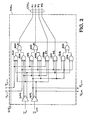
- Fig. 2 is a logic diagram of a representative Booth Encoder shown in block form in Fig. 1, and labelled thereon 266i. Appropriate modifications are required to the circuit shown in Fig. 2 for the Encoders 266a in the first and last rows in the multiplier array 120 and 266p, as will be appreciated by those skilled in the art.
- a pair of inverting amplifiers 500 and 502 receive the signals Yi and Y i+1 , respectively, representing the complement of the i and (i+l)st bit positions of the multiplier operand. Signals Y i-1 and Yi-i are received from the Booth Encoder 266(i-l) in the preceding row (i-1).
- Booth Encoder 266i generates at a true and a complemented output of amplifier 502 the signals Y i+1 and Y i+1 , respectively, which are then conducted to the Booth Encoder 266(i+1) in the next row (i+1).
- Y-i corresponds to a binary ZERO
- the Booth Encoder 266p receives only the Y 30 and Y 31 signals.
- the contents of the three multiplier positions shown in Table I are available to generate the appropriate operation called for in Table I on the signal lines 270i; namely, No_0p (P1, P2, Ml and M2 all LOW), Add Once (P1 HIGH), Add Twice (P2 HIGH), Subtract Once (Ml HIGH) and Subtract Twice (M2 HIGH).
- the Booth Encoder 266i generates the add/subtract control signal on signal line 272i in which a HIGH signal is inserted during a subtract operation and a LOW signal inserted during an add operation.
- the true output of amplifier 500 is connected to a complemented input of an AND gate 504, an AND gate 506 and an AND gate 508.
- the complemented output of amplifier 500 is connected to a complemented input of an AND gate 510, an AND gate 512, and AND gate 514 and an AND gate 516.
- the true output of amplifier 502 is connected to a second complemented input of AND gate 512, AND gate 506, AND gate 514 and a second complemented input of AND gate 518.
- the complemented output of amplifier 502 is connected to a second complemented input of AND gate 510, AND gate 504, and AND gate 508.
- the Y i-1 signal is received at a third complemented input of AND gate 510, AND gate 512, and AND gate 508, while the Y i-1 signal is received at a third complemented input of AND gate 504, AND gate 506, AND gate 514 and a second complemented input of AND gate 518.
- An OR gate 520 receives the outputs of AND gates 510 and 504 and generates at an output the P1 signal which is conducted on one of the signal lines 270i.
- An OR gate 522 receives the outputs of AND gates 512 and 506 and generates at an output the M1 signal which is conducted on a second one of the signal lines 270i.
- the AND gate 5.08 generates at an output the P2 signal which is conducted on a third one of the signal lines 270i, and the AND gate 514 generates at an output the M2 signal which is conducted on a fourth one of the signal lines 270i.
- An OR gate 524 receives the outputs of AND gates 518 and 516 and generates at an output the add/subtract insertion signal which is conducted on the signal line 272i.
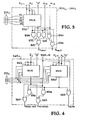
- Fig. 3 is a logic diagram of a representative one of the B cells 200i, ..., 262i, located in the ith row of the array 120 shown in Fig. 1.
- a multiplexer 530 receives on signal lines 270i the P1, Ml, P2 and M2 signals generated by the Booth Encoder 266i in the same row, i, of array 120. These signals are used to select which of the data signals, X J , X i-1 , or binary ZERO, received by the multiplexer 530 will be transmitted to an output of the multiplexer.
- a sum-in (S_IN) signal generated by the B cell in the preceding row via one of the signal lines 350i, ..., 412i is received by the B cell 200i, ..., 262i, respectively.
- the S_IN signal is the add/subtract insertion bit signal generated by the Booth Encoder 266a, 266b, ..., 266p, respectively, conducted therefrom via signal line 272a, 272b, ..., 272p, respectively.
- the carry in (C_IN) signal generated by the B cell in the preceding row is conducted via one of the signal lines 280i, 282i, ..., 340i to the illustrated B cell.
- An input of an AND gate 532, an AND gate 534 and an EXOR gate 536 receive the C_IN signal.
- the signal generated at the output of the multiplexer 530 is received at an input to the AND gate 534, an AND gate 538 and an EXOR gate 540.
- the S_IN signal is received at a second input to AND gate 538.
- AND gate 532 and EXOR gate 540 are examples of the carry in (C_IN) signal generated by the B cell in the preceding row.
- An OR gate 542 receives the signals generated at the outputs of AND gates 532, 534 and 538 and generates therefrom a carry out (C OUT) signal one one of the signal lines 280i, ..., 342i.
- the EXOR gate 536 receives at a second input the signal generated at the output of EXOR gate 540 and generates a sum out (S_OUT) signal on one of the signal lines 350i, ..., 414i.
- the S_OUT and C_OUT signals so generated represent the binary sum and carry out corresponding to the bit position within the ith intermediate sum and carry of the illustrated B cell within the ith row.
- Fig. 4 is a logic diagram of a representative F cell 264i, of the multiplier array 120 shown in Fig. 1.
- a multiplexer receives on signal lines 2701 the P1, M1, P2 and M2 signals generated by the Booth Encoder 266i in the same row, i, of array 120. These signals are used to select which of the sign extended data signals, X i , X i-1 , received on signal lines 418i and 416i, respectively, or binary ZERO, received by the multiplexer 550 will be transmitted to an output of the multiplexer 550, as was described above in connection with the multiplexer 530 contained within the B cell shown in Fig. 3.
- a second multiplexer 552 also receives the Pl, M1, P2 and M2 signals and uses them to select whether the X i or X i , or binary ZERO signal received by the multiplexer 552 will be transmitted to an output of the multiplexer 552.
- SIGN_IN sign-in (SIGN_IN) signal generated by the F cell 264(i-1) in the preceding row (i-1) is received via the signal line 414(i-1).
- This SIGN_IN signal is received at an input to an EXOR gate 554, an input to an AND gate 556 and an input to an AND gate 558.
- the signal generated at the output of the multiplexer 550 is received at a second input to the EXOR gate 554, and a complemented inputs to the AND gates 556 and 558.
- the signal generated at the output of the multiplexer 552 is received at an input to an OR gate 560 and an input to an EXOR gate 562.
- the EXOR gate 554 generates therefrom a SUM OUT signal.
- the EXOR gate 562 receives at a second input the signal generated at the output of AND gate 558 generates at an output a GUARD signal.
- the OR gate 560 receives at a second input the signal generated at the output of the AND gate 556 and generates at an output a SIGN_OUT signal.
- the SIGN_OUT signal so generated is conducted via signal line 4141 to the F cell 264(i+I), in the next row of array 120.
- the F cell 264i of the instant invention provides the capability of retaining only this minimal amount of sign extension bit information without retaining all the extraneous sign extension bits forming the bit positions to their left. In this manner, the compact multiplier array 120 can efficiently generate the intermediate products by providing just enough storage.
- the design of the novel F cell 264i illustrated in Fig. 4 affords the compact multiplier array 120 of the present invention by recognizing that the potential overflow of an intermediate sum can be managed in suitably modifying the design of the B cell, and incorporating therein a suitably redesigned second B cell.
- the carry in (C_IN) signal to the F cell is established at a level corresponding to a binary ZERO and circuitry corresponding to a first B cell sums X i-1 and SIGN_IN with a carry in of ZERO. This is reflected in the design shown in Fig.
- Circuitry corresponding to a second B cell sums the SIGN_IN and X J signals.
- multiplier array 120 of the instant invention is perhaps best understood by reference to the following example in which the size of the two's complement multiplicand and multiplier words are reduced from 32 bits to eight bits, to facilitate the description.
- the two's complement binary representation of a multiplicand equal to -76 is on the first line of the example.
- the binary representation of a multiplier equal to +85 is on the second line.
- the multiplicand, with the sign bit extended through the three next-most significant positions, is shown on line three of the example. Sign extension is performed by the F cell 264a.
- On line four are the inserted add/subtract bits which are generated by the Booth Encoders 266a, ..., 266p and included in the summations performed by the B cells 200a, 204a, ..., 262a in the first row of array 120. This quantity is sign-extended through the two next-most significant positions.
- the values of Y-1, Yo, and Yi, are 0, 1, 0, respectively, and in accordance with Table I, the operation of -2X is performed on the multiplicand X.
- the Booth Encoder 266a generates the M2 signal as a HIGH, and the multiplexers 530 of the B cells in the second row accordingly select the left-shifted X 1 operands as do the multiplexers 550 and 552 of the F cell 264b in the second row.
- the sixth and seventh lines represent the sum and carry bits resulting from summing lines three, four, and five. These "carry-save" operations are performed by the F cell and the B cells in the second row of array 120, and the resulting sum and carry signals represent the first intermediate sum and carry.
- Line eight represents the -IX operation performed by the B and F cells in the third row of array 120 as selected by the Ml HIGH signal generated by Booth Encoder cell 266c.
- a second intermediate sum and carry is generated by these B and F cells 200c, ..., 264c as is shown on lines nine and ten of the example.
- Another -IX operation and a third intermediate sum and carry is shown on lines eleven, twelve and thirteen of the example. These operations are performed by the B and F cells 200d, ..., 264d as directed by the Booth Encoder cell 266d in the fourth row of array 120.
- Line fourteen shows the results of a +1X operation performed by the F and B cells 200e, ..., 264e of the fifth row of array 120 as selected by the Booth Encoder cell 266e.
- Line fifteen of the example is the complete 16-bit product of the multiplicand (-76) and the multiplier (+85). It is the two's complement binary representation of -6460. As mentioned above, this product is formed in registers external to the multiplier array 120.
Landscapes
- Physics & Mathematics (AREA)
- General Physics & Mathematics (AREA)
- Computational Mathematics (AREA)
- Mathematical Analysis (AREA)
- Mathematical Optimization (AREA)
- Pure & Applied Mathematics (AREA)
- Engineering & Computer Science (AREA)
- Theoretical Computer Science (AREA)
- Computing Systems (AREA)
- General Engineering & Computer Science (AREA)
- Complex Calculations (AREA)
- Image Generation (AREA)
Applications Claiming Priority (2)
| Application Number | Priority Date | Filing Date | Title |
|---|---|---|---|
| US747073 | 1985-06-19 | ||
| US06/747,073 US4748582A (en) | 1985-06-19 | 1985-06-19 | Parallel multiplier array with foreshortened sign extension |
Publications (2)
| Publication Number | Publication Date |
|---|---|
| EP0206762A2 true EP0206762A2 (de) | 1986-12-30 |
| EP0206762A3 EP0206762A3 (de) | 1988-02-10 |
Family
ID=25003553
Family Applications (1)
| Application Number | Title | Priority Date | Filing Date |
|---|---|---|---|
| EP86304707A Withdrawn EP0206762A3 (de) | 1985-06-19 | 1986-06-18 | Digitale elektronische Multiplizierschaltungen |
Country Status (3)
| Country | Link |
|---|---|
| US (1) | US4748582A (de) |
| EP (1) | EP0206762A3 (de) |
| JP (1) | JPS61296429A (de) |
Cited By (6)
| Publication number | Priority date | Publication date | Assignee | Title |
|---|---|---|---|---|
| FR2611286A1 (fr) * | 1987-02-23 | 1988-08-26 | Dassault Electronique | Circuit integre multiplieur, et son procede de composition |
| EP0297989A3 (de) * | 1987-06-30 | 1989-12-27 | Digital Equipment Corporation | Einrichtung und Verfahren zur Beschleunigung Ganzzahl- oder Gleitpunktmultiplikationprozedur |
| EP0291356A3 (en) * | 1987-05-15 | 1990-01-10 | Digital Equipment Corporation | Apparatus and method for performing a shift operation in a multiplier array circuit |
| EP0295621A3 (de) * | 1987-06-15 | 1991-01-09 | Nec Corporation | Schnelle Summierschaltung |
| EP0314968A3 (de) * | 1987-11-03 | 1991-05-08 | International Business Machines Corporation | Überlappendes Mehrbit untersuchendes Multipliziersystem mit einer Bandmatrix von Teilprodukten |
| EP0448367A3 (en) * | 1990-03-20 | 1993-01-07 | Fujitsu Limited | High speed digital parallel multiplier |
Families Citing this family (17)
| Publication number | Priority date | Publication date | Assignee | Title |
|---|---|---|---|---|
| JPS63241634A (ja) * | 1987-03-30 | 1988-10-06 | Toshiba Corp | 並列型加算回路 |
| US4843585A (en) * | 1987-09-14 | 1989-06-27 | Motorola, Inc. | Pipelineable structure for efficient multiplication and accumulation operations |
| US4910701A (en) * | 1987-09-24 | 1990-03-20 | Advanced Micro Devices | Split array binary multiplication |
| US4926371A (en) * | 1988-12-28 | 1990-05-15 | International Business Machines Corporation | Two's complement multiplication with a sign magnitude multiplier |
| US5038315A (en) * | 1989-05-15 | 1991-08-06 | At&T Bell Laboratories | Multiplier circuit |
| US5195051A (en) * | 1992-03-31 | 1993-03-16 | Intel Corporation | Computation of sign bit and sign extension in the partial products in a floating point multiplier unit |
| US5781457A (en) * | 1994-03-08 | 1998-07-14 | Exponential Technology, Inc. | Merge/mask, rotate/shift, and boolean operations from two instruction sets executed in a vectored mux on a dual-ALU |
| US5442577A (en) * | 1994-03-08 | 1995-08-15 | Exponential Technology, Inc. | Sign-extension of immediate constants in an alu |
| US5867414A (en) * | 1994-08-17 | 1999-02-02 | Industrial Technology Research Institute | Compact pipelined matrix multiplier utilizing encoding and shifting circuit configurations |
| US5825679A (en) * | 1995-09-11 | 1998-10-20 | Digital Equipment Corporation | Fast sign extend for multiplier array sums and carrys |
| US5729485A (en) * | 1995-09-11 | 1998-03-17 | Digital Equipment Corporation | Fast determination of carry inputs from lower order product for radix-8 odd/even multiplier array |
| US6055619A (en) * | 1997-02-07 | 2000-04-25 | Cirrus Logic, Inc. | Circuits, system, and methods for processing multiple data streams |
| US6259957B1 (en) | 1997-04-04 | 2001-07-10 | Cirrus Logic, Inc. | Circuits and methods for implementing audio Codecs and systems using the same |
| US6684236B1 (en) * | 2000-02-15 | 2004-01-27 | Conexant Systems, Inc. | System of and method for efficiently performing computations through extended booth encoding of the operands thereto |
| US7797366B2 (en) * | 2006-02-15 | 2010-09-14 | Qualcomm Incorporated | Power-efficient sign extension for booth multiplication methods and systems |
| US7809783B2 (en) * | 2006-02-15 | 2010-10-05 | Qualcomm Incorporated | Booth multiplier with enhanced reduction tree circuitry |
| US8392174B2 (en) * | 2006-08-07 | 2013-03-05 | International Characters, Inc. | Method and apparatus for lexical analysis using parallel bit streams |
Family Cites Families (4)
| Publication number | Priority date | Publication date | Assignee | Title |
|---|---|---|---|---|
| US3878985A (en) * | 1973-11-30 | 1975-04-22 | Advanced Micro Devices Inc | Serial-parallel multiplier using booth{3 s algorithm with combined carry-borrow feature |
| JPS57141753A (en) * | 1981-02-25 | 1982-09-02 | Nec Corp | Multiplication circuit |
| FR2546318B1 (fr) * | 1983-05-20 | 1987-12-24 | Efcis | Multiplieur binaire avec extension de signe pour la multiplication de nombres signes ou non signes |
| US4644488A (en) * | 1983-10-12 | 1987-02-17 | California Institute Of Technology | Pipeline active filter utilizing a booth type multiplier |
-
1985
- 1985-06-19 US US06/747,073 patent/US4748582A/en not_active Expired - Lifetime
-
1986
- 1986-06-18 JP JP61143978A patent/JPS61296429A/ja active Pending
- 1986-06-18 EP EP86304707A patent/EP0206762A3/de not_active Withdrawn
Cited By (7)
| Publication number | Priority date | Publication date | Assignee | Title |
|---|---|---|---|---|
| FR2611286A1 (fr) * | 1987-02-23 | 1988-08-26 | Dassault Electronique | Circuit integre multiplieur, et son procede de composition |
| EP0291356A3 (en) * | 1987-05-15 | 1990-01-10 | Digital Equipment Corporation | Apparatus and method for performing a shift operation in a multiplier array circuit |
| EP0295621A3 (de) * | 1987-06-15 | 1991-01-09 | Nec Corporation | Schnelle Summierschaltung |
| EP0297989A3 (de) * | 1987-06-30 | 1989-12-27 | Digital Equipment Corporation | Einrichtung und Verfahren zur Beschleunigung Ganzzahl- oder Gleitpunktmultiplikationprozedur |
| EP0314968A3 (de) * | 1987-11-03 | 1991-05-08 | International Business Machines Corporation | Überlappendes Mehrbit untersuchendes Multipliziersystem mit einer Bandmatrix von Teilprodukten |
| EP0448367A3 (en) * | 1990-03-20 | 1993-01-07 | Fujitsu Limited | High speed digital parallel multiplier |
| US5465226A (en) * | 1990-03-20 | 1995-11-07 | Fujitsu Limited | High speed digital parallel multiplier |
Also Published As
| Publication number | Publication date |
|---|---|
| US4748582A (en) | 1988-05-31 |
| EP0206762A3 (de) | 1988-02-10 |
| JPS61296429A (ja) | 1986-12-27 |
Similar Documents
| Publication | Publication Date | Title |
|---|---|---|
| EP0206762A2 (de) | Digitale elektronische Multiplizierschaltungen | |
| US3993891A (en) | High speed parallel digital adder employing conditional and look-ahead approaches | |
| US6564239B2 (en) | Computer method and apparatus for division and square root operations using signed digit | |
| US6523055B1 (en) | Circuit and method for multiplying and accumulating the sum of two products in a single cycle | |
| US6446104B1 (en) | Double precision floating point multiplier having a 32-bit booth-encoded array multiplier | |
| US4168530A (en) | Multiplication circuit using column compression | |
| CA1096048A (en) | Floating point data processor | |
| EP0018519B1 (de) | Multipliziereinrichtung, die einen Addierer mit Übertrags-Speicherung/- Fortpflanzung enthält | |
| US4179734A (en) | Floating point data processor having fast access memory means | |
| Cooper | Parallel architecture modified Booth multiplier | |
| US5206823A (en) | Apparatus to perform Newton iterations for reciprocal and reciprocal square root | |
| US5220524A (en) | Machine method to perform newton iterations for reciprocals | |
| JPH0727456B2 (ja) | 浮動小数点演算装置 | |
| US4354249A (en) | Processing unit for multiplying two mathematical quantities including at least one complex multiplier | |
| EP0040279B1 (de) | Binärer Dividierer | |
| US3535498A (en) | Matrix of binary add-subtract arithmetic units with bypass control | |
| EP0416308A2 (de) | Rechteckiger Matrixstrukturierter Vorzeichenziffernmultiplizierer | |
| EP0295788B1 (de) | Einrichtung und Verfahren für eine erweiterte Arithmetik-Logik-Einheit zur Beschleunigung der ausgewählten Operationen | |
| KR100308726B1 (ko) | 고속 산술 장치에서 올림수 예견가산기 스테이지의 수를 감소시키는 장치 및 방법 | |
| US5721697A (en) | Performing tree additions via multiplication | |
| US7337202B2 (en) | Shift-and-negate unit within a fused multiply-adder circuit | |
| US3840727A (en) | Binary multiplication by addition with non-verlapping multiplier recording | |
| EP0529755B1 (de) | Verfahren und Anordnung zur Negierung eines Multiplikationsoperanden | |
| US5206826A (en) | Floating-point division cell | |
| EP0534760A2 (de) | Hochgeschwindigkeitsmultiplizierer |
Legal Events
| Date | Code | Title | Description |
|---|---|---|---|
| PUAI | Public reference made under article 153(3) epc to a published international application that has entered the european phase |
Free format text: ORIGINAL CODE: 0009012 |
|
| AK | Designated contracting states |
Kind code of ref document: A2 Designated state(s): AT BE CH DE FR GB IT LI LU NL SE |
|
| PUAL | Search report despatched |
Free format text: ORIGINAL CODE: 0009013 |
|
| AK | Designated contracting states |
Kind code of ref document: A3 Designated state(s): AT BE CH DE FR GB IT LI LU NL SE |
|
| 17P | Request for examination filed |
Effective date: 19880223 |
|
| 17Q | First examination report despatched |
Effective date: 19890601 |
|
| STAA | Information on the status of an ep patent application or granted ep patent |
Free format text: STATUS: THE APPLICATION IS DEEMED TO BE WITHDRAWN |
|
| 18D | Application deemed to be withdrawn |
Effective date: 19891212 |
|
| RIN1 | Information on inventor provided before grant (corrected) |
Inventor name: NEW, BERNARD Inventor name: FLAHERTY, TIMOTHY |