EP0206764A1 - Fabrication de guides d'ondes optiques - Google Patents
Fabrication de guides d'ondes optiques Download PDFInfo
- Publication number
- EP0206764A1 EP0206764A1 EP86304714A EP86304714A EP0206764A1 EP 0206764 A1 EP0206764 A1 EP 0206764A1 EP 86304714 A EP86304714 A EP 86304714A EP 86304714 A EP86304714 A EP 86304714A EP 0206764 A1 EP0206764 A1 EP 0206764A1
- Authority
- EP
- European Patent Office
- Prior art keywords
- layer
- optical waveguide
- refractive index
- guiding layer
- substrate
- Prior art date
- Legal status (The legal status is an assumption and is not a legal conclusion. Google has not performed a legal analysis and makes no representation as to the accuracy of the status listed.)
- Granted
Links
Images




Classifications
-
- C—CHEMISTRY; METALLURGY
- C03—GLASS; MINERAL OR SLAG WOOL
- C03C—CHEMICAL COMPOSITION OF GLASSES, GLAZES OR VITREOUS ENAMELS; SURFACE TREATMENT OF GLASS; SURFACE TREATMENT OF FIBRES OR FILAMENTS MADE FROM GLASS, MINERALS OR SLAGS; JOINING GLASS TO GLASS OR OTHER MATERIALS
- C03C17/00—Surface treatment of glass, not in the form of fibres or filaments, by coating
- C03C17/02—Surface treatment of glass, not in the form of fibres or filaments, by coating with glass
-
- G—PHYSICS
- G02—OPTICS
- G02B—OPTICAL ELEMENTS, SYSTEMS OR APPARATUS
- G02B6/00—Light guides; Structural details of arrangements comprising light guides and other optical elements, e.g. couplings
- G02B6/10—Light guides; Structural details of arrangements comprising light guides and other optical elements, e.g. couplings of the optical waveguide type
- G02B6/12—Light guides; Structural details of arrangements comprising light guides and other optical elements, e.g. couplings of the optical waveguide type of the integrated circuit kind
- G02B6/13—Integrated optical circuits characterised by the manufacturing method
Definitions
- the present invention relates to the fabrication of optical waveguides, and in particular to the fabrication of optical waveguides in integrated optical circuits.
- Such optical waveguides have been made by flame hydrolysis, as described in US patent no 3,806,223 of Keck et al.
- fine glass particles are produced as a soot from the flame of a gas burner which is fed with SiC1 4 .
- the soot is deposited on a substrate, such as fused silica, having the appropriate optical and mechanical properties.
- a less heavily doped silica layer is then formed over the layer of doped soot.
- the structure is sintered at about 1500°C to vitrify and densify the sooty layers.
- UK patent application no 2066805A teaches the use of a furnace in place of a gas burner to hydrolyse halides of Si and Ti, B, P, or Ge, together with oxygen or steam to produce fine glass particles on a substrate heated to 600 - 1100 0 C. Vitrification involved heating the substrate to 1300 - 1600°C.
- PECVD plasma enhanced chemical vapour deposition
- silicon oxynitride produced by CVD, has an unacceptable degree of surface roughness which must be reduced by reflowing at high temperature to reduce scatter loss. Internal defects also occur in CVD silicon nitride and oxynitride, and these too can give rise to high losses unless annealed out (a C0 2 laser was used for this by Lam).
- a method of fabricating a waveguide comprising the steps of forming a layer of arsenosilicate glass on a substrate.
- an optical waveguide comprising a guiding layer of arsenosilicate glass.
- arsenosilicate glass is suitable for use as a waveguide, and, moreover, offers surprisingly low loss in the near infra red, despite the fact that the glass is made from hydrides (SiH 4 and AsH 3 ) which would be expected to give rise to large losses in the near infra-red.
- the refractive index of the as deposited film varies with arsenic content, between about 1.53 for 12 0 /o As to about 1.45 for 1.7 0 /o As.
- ASG suitable for use as a guiding layer with silica (n 1.46) cladding, and also enabling the production of waveguides in which the cladding and guiding layers are each made of ASG.
- Arsenosilicate glass is thus preferable to silicon nitride (n 2.01) for use with Si0 2 , since a large refractive index difference necessitates the use of very thin waveguides if only low order modes are to be supported.
- Arsenosilicate glass is an arsenic doped form of silicon dioxide, and is conventionally produced by reacting silane (SiH 4 ), arsine (AsH 3 ) and oxygen in a CYD reactor.
- the reaction is a homogeneous gas phase reaction and hence the ASG is deposited with a rough surface which needs to be reflowed to reduce scatter loss to an acceptably low level.
- Arsenic reduces the melting point of silicon dioxide, the melting point decreasing progressively with an increasing concentration of dopant, so that ASG with more than about 10 0 /o As can be reflowed at temperatures as low as 800/900°C ( in steam).
- Arsenic is present in ASG in the form of arsenic trioxide (As 2 0 3 ) which has a significant vapour pressure over ASG and it can readily be lost by evaporation when the glass is heated. Because of this, the arsenic content of the glass drops during reflowing as a result of which the refractive index also falls. The loss of arsenic is not uniform throughout the thickness of the film; the greatest amount is lost from the surface layers, as will be explained in greater detail below.
- waveguides can be made by depositing ASG using conventional processes, it is preferably deposited according to the method described in our copending European application number 85300172.5 filed 10 January 1985, and published under the number 0150088.
- the reaction can be carried out at temperatures down to below 400°C without the use of a plasma, and by virtue of the reaction mechanism, the ASG is deposited with a much smoother surface than is achieved with conventional processes.
- the as deposited density is also improved compared to that of conventional ASG.
- the ASG can be baked at 600-900 * C to further densify and reflow the layer.
- ASG deposited as the result of the modified, heterogeneous reaction The advantages of using ASG deposited as the result of the modified, heterogeneous reaction are that the substrate need not be exposed to high temperatures, no plasma is needed; and the smooth surface produced by the reaction gives rise to low scatter loss, even without being reflowed.
- the ASG is produced in a chemical vapour deposition (CVD) process such as may be carried out in a commercial CV& machine.
- CVD chemical vapour deposition
- Machines designed for the silane-oxygen reaction for CYD of silicon dioxide such as the PYROX Reactor produced by Tempress-Xynetics, are particularly suitable for carrying out the ASG deposition, although other machines may also be suitable.
- PYROX 216 Reactor is to be used, and such a reactor is shown diagrammatically Figure 1.
- the PYROX Reactor which provides for batch processing of wafers, has a water cooled 102 reactor head 100 within which there is a rotatable circular table 101 upon which are placed wafers 103 to be treated.
- the table 101 which supports a graphite wafer carrier 104, is heated from underneath during processing, the temperature of the table 101 and hence of the wafers being measured by means of a thermocouple. In the experiments to be reported, three-inch wafers were used. The wafers were held on silicon carbide coated graphite succeptors 99, arranged in a circle of twelve around the outer ring of an eighteen wafer carrier.
- the reactor head consists of four concentric zones which, moving out from the centre, are termed A, B, C, and D.
- the gas flow to each of these zones can be adjusted to vary the conditions within the reactor head.
- Separate flow control valves 105, 106 and 107 and pressure gauges 108, 109, and 110 are provided for zones A, B, and C; flow to Zone D is not independently controllable.
- the composition of the gas fed to the reactor head can be adjusted by flow control valves 111-116 in each of six flowlines, the flowrates in each of the flowlines being monitored by means of rotameters 117-122, containing floats 123-128. In the present case, only five flowlines are required:
- the deposition rate is limited by the diffusion rate of the reactants through a very thin depleted zone near the surface which will follow the contours of the surface.
- the silane and oxygen system shows a very small dependence of deposition rate on temperature (in the example illustrated it is practically constant at 9A per °C, which is small when compared to the 29A per °C to 63 0 A per °C for the arsine-silane-oxygen example shown) and the lack of any diffusion limit indicates that it is homogeneous gas phase reaction.
- the reaction mechanism determines the type of species that will arrive at the surface. If the reaction is homogeneous, the oxygen and silane react to form silicon dioxide, or a similar species, in the gas phase. These molecules may condense in the gas phase to form colloidal particles.
- the silicon dioxide will arrive at the surface as particles ranging in size from the monomer to colloidal particles, giving rise to the characteristic rough pebble - like texture of low temperature CVD oxides, as shown in Figure 4.
- the reaction parameters such as pressure and gas composition will control the particle size distribution and hence the surface texture. The mobility of these particles will be small and decrease with increasing particle size.
- heterogeneous reaction The significance of the heterogeneous reaction is that the deposition rate is controlled by the surface temperature and not by the geometry of the surface, and hence one may expect such a reaction to give conformal oxide coatings. Moreover in a heterogeneous reaction the silane and oxygen are absorbed onto a surface where they subsequently react to form silicon dioxide. As these absorbed species will be very mobile, good step coverage and smooth surfaces should result.
- Figure 5 shows the smooth surface produced as a result of heterogeneous reaction, and should be compared with Figure 4 which shows a typical equivalent (PSG) deposited from a homogeneous reaction.
- Figure 6 shows a conformal coating 50 of ASG . over a l u m high aluminium track 51 with near vertical side walls 52.
- Figure 7 shows a typical non-conformal coating 60 produced as a result of a homogeneous reaction between silane and oxygen.
- the results of the homogeneous reaction can be seen as overhangs 61 and 62 at the sides of the track 51; such overhangs are typical of the non-conformal deposition which characterises homogeneous reactions.
- the As 2 O 3 content of the glasses produced under heterogeneous reaction conditions were as follows:
- the films will reflow in 0 2 , steam and POCl 3 /O 2 .
- To achieve the same degree of planarization films that are reflowed in steam require temperatures about 100°C lower than those reflowed in POCl 3 /0 2 .
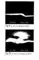
- Figures 9 and 10 show the cross section of ASG films (8000A 17 mole %As 2 O 3 ) that have been deposited on polysilicon steps (5000A high with plasma etched near vertical walls) and reflowed in steam for 15 minutes.
- the film in Figure 9 was flowed at 800°C and that in Figure 10 at 900°C.
- Films deposited directly onto silicon should not be baked in pure nitrogen or argon, as this may lead to the formation of elemental arsenic at the ASG/silicon interface.
- arsenic trioxide As 2 0 3
- ASG arsenic trioxide
- infrared spectrophotometry is the popular technique for rapid routine determinations.
- a calibration graph for ASG films, which relates absorption peak intensities to film composition has been generated by Wong and Ghezzo (J Electrochem Soc V118, No 9, p1540, 1971) who used the X-ray microprobe analysis of the films and the flame spectrophotometric analysis of the dissolved films as calibration standards.
- the IR results were calculated using Wong and Ghezzo's calibration chart for as-deposited ASG films.
- FIG. 13 A typical result from a film that contained an initial concentration of 13 mole% As 2 0 3 is shown in Figure 13.
- the graph clearly shows the concentration gradient caused by the diffusion of A S2 0 3 from the surface.
- the P 2 0 5 generated during the back gettering step can be seen diffusing from the surface into the film creating a near-surface layer of arsonophosphosilicate glass which should give the film better gettering properties.
- Arsenosilicate glass containing 12 mole % arsenic was deposited, under heterogeneous reaction conditions (mass transport limited region) on a 3" silica wafer (type Q2 3W53.10.C, made by the Hoya corporation) to a depth of 2 ⁇ m at a temperature of 450°C, at a rate of 400A per minute.
- a reference silicon wafer was also coated at the same time, and the ASG thickness measured on that by optical interference techniques. The thickness was found to vary by about ⁇ 3% across the 3" wafer.
- a prism coupler and helium neon (6328A) laser were used to determine the filmthickness and refractive index of the film on the silica wafer. The thickness measurements agreed with that carried out on the silicon wafer.
- the film was found to be bimodal (at 6328A).
- the effective index of the zero order TE and TM modes was found to be 1.502, and that of the first order TE and TM modes 1.477.
- the bulk refractive index of the film calculated to be about 1.53, about 0.07 above that of silica, and agrees well with that measured on the similar film on silicon.
- the decay of the scattered light (6328A) along the propagating beam was measured and losses of between 0.3 and 0.5dB cm -1 for the fundamental mode, and 0.8 to 1.2dB cm -1 for the first order mode were determined. Examination of the uncoupled reflected light beam indicate a very low level of scatter loss.
- a simple waveguide can be made with just a guiding layer of ASG on a silica or other suitable substrate.
- ASG is also well suited to manufacture of buried waveguide devices. Because surface scatter loss is dependent upon the refractive index difference across the surface, buried waveguides, which reduce that difference can have reduced scatter loss. As can be seen from Figure 14, it is possible to vary the refractive index of ASG between about 1.45 and 1.53 by varying the arsenic content between about 2 and 12%.
- A2.5 ⁇ m layer of ASG containing 10 mole percent A s2 0 3 (n ⁇ 1.52) was deposited on a silica slice.
- a 500A layer of aluminium was evaporated onto the back of the substrate to facilitate mask alignment.
- a 1 ⁇ m layer of positive resist was spun onto the ASG layer.
- the waveguide pattern was then printed using a contact mask, and the resist developed to define the pattern.
- the ASG layer was plasma etched in a C 2 F 6 /GHF 3 /He atmosphere (oxygen being excluded to prevent erosion of the resist mask). The remaining resist was stripped. Finally the aluminium was removed from the rear side.
- Waveguides produced by this technique are shown in Figures 15 and 16. Of particular note are the waveguides's very smooth top and its freedom from edge ripple. Figure 16 clearly shows the waveguide's smooth sides.
- Adopting a coventional approach to the fabrication of a buried waveguide structure two separate ASG layers may be provided.
- a heavily doped layer with 10-12 mole % arsenic, 2 um thick is deposited for the guiding layer.
- a passive device structure such as a ring resonator, beam splitter, or coupler etc can be formed in the first layer.
- a second layer with 2-4°/o arsenic, 3pm thick is deposited to bury the first.
- plasma etching it may be necessary to briefly reflow the first ASG layer to remove wall roughness before depositing the second layer.
- reaction temperature can be reduced to about 390°C.
- the reaction temperature can be reduced to about 390°C.
- the ASG can be deposited at temperatures between about 390 and 450°C, provided no reflowing is required it can be used in conjunction with III-V semiconductors.
- a suitable buffer layer which could be a low arsenic ASG layer
- ASG may be deposited on a substrate of III-V material.
- ASG with a lower index cladding of an optically active material, eg an optically active organic material.
Landscapes
- Engineering & Computer Science (AREA)
- Chemical & Material Sciences (AREA)
- Physics & Mathematics (AREA)
- General Physics & Mathematics (AREA)
- Optics & Photonics (AREA)
- Life Sciences & Earth Sciences (AREA)
- Microelectronics & Electronic Packaging (AREA)
- Chemical Kinetics & Catalysis (AREA)
- General Chemical & Material Sciences (AREA)
- Geochemistry & Mineralogy (AREA)
- Materials Engineering (AREA)
- Organic Chemistry (AREA)
- Optical Integrated Circuits (AREA)
- Glass Melting And Manufacturing (AREA)
- Glass Compositions (AREA)
Priority Applications (1)
| Application Number | Priority Date | Filing Date | Title |
|---|---|---|---|
| AT86304714T ATE50974T1 (de) | 1985-06-21 | 1986-06-19 | Herstellung von optischen wellenleitern. |
Applications Claiming Priority (2)
| Application Number | Priority Date | Filing Date | Title |
|---|---|---|---|
| GB8515814 | 1985-06-21 | ||
| GB858515814A GB8515814D0 (en) | 1985-06-21 | 1985-06-21 | Fabrication of optical waveguides |
Publications (2)
| Publication Number | Publication Date |
|---|---|
| EP0206764A1 true EP0206764A1 (fr) | 1986-12-30 |
| EP0206764B1 EP0206764B1 (fr) | 1990-03-14 |
Family
ID=10581165
Family Applications (1)
| Application Number | Title | Priority Date | Filing Date |
|---|---|---|---|
| EP86304714A Expired - Lifetime EP0206764B1 (fr) | 1985-06-21 | 1986-06-19 | Fabrication de guides d'ondes optiques |
Country Status (8)
| Country | Link |
|---|---|
| US (1) | US4946251A (fr) |
| EP (1) | EP0206764B1 (fr) |
| JP (1) | JP2594046B2 (fr) |
| AT (1) | ATE50974T1 (fr) |
| AU (1) | AU590886B2 (fr) |
| DE (1) | DE3669494D1 (fr) |
| GB (1) | GB8515814D0 (fr) |
| WO (1) | WO1986007588A1 (fr) |
Cited By (5)
| Publication number | Priority date | Publication date | Assignee | Title |
|---|---|---|---|---|
| US4904616A (en) * | 1988-07-25 | 1990-02-27 | Air Products And Chemicals, Inc. | Method of depositing arsine, antimony and phosphine substitutes |
| US4988640A (en) * | 1988-07-25 | 1991-01-29 | Air Products And Chemicals, Inc. | Method of doping and implanting using arsine, antimony, and phosphine substitutes |
| US5124278A (en) * | 1990-09-21 | 1992-06-23 | Air Products And Chemicals, Inc. | Amino replacements for arsine, antimony and phosphine |
| US7548364B2 (en) | 2006-07-31 | 2009-06-16 | Applied Materials, Inc. | Ultra-fast beam dithering with surface acoustic wave modulator |
| US7569463B2 (en) | 2006-03-08 | 2009-08-04 | Applied Materials, Inc. | Method of thermal processing structures formed on a substrate |
Families Citing this family (8)
| Publication number | Priority date | Publication date | Assignee | Title |
|---|---|---|---|---|
| TW263566B (fr) * | 1993-01-14 | 1995-11-21 | Sumitomo Electric Industries | |
| JP2739806B2 (ja) * | 1993-06-08 | 1998-04-15 | 日本電気株式会社 | 光導波路の製造方法 |
| FR2727768B1 (fr) * | 1994-12-05 | 1997-01-10 | Alcatel Nv | Procede pour former une couche de silice a eliminer ulterieurement et procede pour rapporter un composant en optique integree |
| JP3270353B2 (ja) * | 1997-03-05 | 2002-04-02 | 日本電気株式会社 | 光導波路の製造方法 |
| US5852687A (en) * | 1997-07-09 | 1998-12-22 | Trw Inc. | Integrated optical time delay unit |
| JP2001281487A (ja) * | 2000-03-30 | 2001-10-10 | Furukawa Electric Co Ltd:The | 光導波路装置およびその製造方法 |
| AUPR178200A0 (en) * | 2000-11-29 | 2000-12-21 | Redfern Integrated Optics Pty Ltd | Silica-based optical device fabrication |
| KR101323222B1 (ko) * | 2006-03-08 | 2013-10-30 | 어플라이드 머티어리얼스, 인코포레이티드 | 기판상에 형성되는 구조체의 열적 프로세싱을 위한 장치 및 방법 |
Citations (2)
| Publication number | Priority date | Publication date | Assignee | Title |
|---|---|---|---|---|
| EP0052901A1 (fr) * | 1980-11-25 | 1982-06-02 | Koninklijke Philips Electronics N.V. | Procédé de fabrication de circuits de guides d'ondes optiques intégrés et circuits obtenus par ledit procédé de fabrication |
| EP0106752A1 (fr) * | 1982-10-05 | 1984-04-25 | COMPAGNIE LYONNAISE DE TRANSMISSIONS OPTIQUES Société anonyme dite: | Procédé de fabrication de guides d'ondes lumineuses |
Family Cites Families (8)
| Publication number | Priority date | Publication date | Assignee | Title |
|---|---|---|---|---|
| US4067641A (en) * | 1974-01-18 | 1978-01-10 | Texas Instruments Incorporated | Waveguide for integrated optical circuits |
| US3957342A (en) * | 1974-07-29 | 1976-05-18 | The Post Office | Sodium borosilicate glasses for dielectric optical waveguides |
| JPS5145543A (en) * | 1974-10-17 | 1976-04-19 | Nippon Telegraph & Telephone | Hikaridoharo oyobi sonoseizohoho |
| GB1546828A (en) * | 1976-07-01 | 1979-05-31 | Secr Defence | Infra red transmitting glass member |
| AU520414B2 (en) * | 1977-06-07 | 1982-01-28 | International Standard Electric Corp. | Optical fibres |
| US4355454A (en) * | 1979-09-05 | 1982-10-26 | Texas Instruments Incorporated | Coating device with As2 -O3 -SiO2 |
| US4585299A (en) * | 1983-07-19 | 1986-04-29 | Fairchild Semiconductor Corporation | Process for fabricating optical wave-guiding components and components made by the process |
| US4666247A (en) * | 1985-02-08 | 1987-05-19 | American Telephone And Telegraph Company, At&T Bell Laboratories | Multiconstituent optical fiber |
-
1985
- 1985-06-21 GB GB858515814A patent/GB8515814D0/en active Pending
-
1986
- 1986-06-18 AU AU58974/86A patent/AU590886B2/en not_active Ceased
- 1986-06-19 WO PCT/GB1986/000357 patent/WO1986007588A1/fr not_active Ceased
- 1986-06-19 JP JP61503549A patent/JP2594046B2/ja not_active Expired - Lifetime
- 1986-06-19 AT AT86304714T patent/ATE50974T1/de not_active IP Right Cessation
- 1986-06-19 DE DE8686304714T patent/DE3669494D1/de not_active Expired - Lifetime
- 1986-06-19 EP EP86304714A patent/EP0206764B1/fr not_active Expired - Lifetime
-
1989
- 1989-09-05 US US07/403,069 patent/US4946251A/en not_active Expired - Lifetime
Patent Citations (2)
| Publication number | Priority date | Publication date | Assignee | Title |
|---|---|---|---|---|
| EP0052901A1 (fr) * | 1980-11-25 | 1982-06-02 | Koninklijke Philips Electronics N.V. | Procédé de fabrication de circuits de guides d'ondes optiques intégrés et circuits obtenus par ledit procédé de fabrication |
| EP0106752A1 (fr) * | 1982-10-05 | 1984-04-25 | COMPAGNIE LYONNAISE DE TRANSMISSIONS OPTIQUES Société anonyme dite: | Procédé de fabrication de guides d'ondes lumineuses |
Non-Patent Citations (1)
| Title |
|---|
| CHEMICAL ABSTRACTS, vol. 77, no. 16, 16 October 1972, page 216, abstract no. 105012y, Columbus, Ohio, US; J. WONG: "Vapor deposition and properties of binary arsenosilicate glass films", & J. ELECTROCHEM. SOC. 1972, 119(8), 1071-80 * |
Cited By (7)
| Publication number | Priority date | Publication date | Assignee | Title |
|---|---|---|---|---|
| US4904616A (en) * | 1988-07-25 | 1990-02-27 | Air Products And Chemicals, Inc. | Method of depositing arsine, antimony and phosphine substitutes |
| US4988640A (en) * | 1988-07-25 | 1991-01-29 | Air Products And Chemicals, Inc. | Method of doping and implanting using arsine, antimony, and phosphine substitutes |
| US5124278A (en) * | 1990-09-21 | 1992-06-23 | Air Products And Chemicals, Inc. | Amino replacements for arsine, antimony and phosphine |
| US7569463B2 (en) | 2006-03-08 | 2009-08-04 | Applied Materials, Inc. | Method of thermal processing structures formed on a substrate |
| US10141191B2 (en) | 2006-03-08 | 2018-11-27 | Applied Materials, Inc. | Method of thermal processing structures formed on a substrate |
| US10840100B2 (en) | 2006-03-08 | 2020-11-17 | Applied Materials, Inc. | Method of thermal processing structures formed on a substrate |
| US7548364B2 (en) | 2006-07-31 | 2009-06-16 | Applied Materials, Inc. | Ultra-fast beam dithering with surface acoustic wave modulator |
Also Published As
| Publication number | Publication date |
|---|---|
| DE3669494D1 (de) | 1990-04-19 |
| AU590886B2 (en) | 1989-11-23 |
| GB8515814D0 (en) | 1985-07-24 |
| US4946251A (en) | 1990-08-07 |
| JPS63500272A (ja) | 1988-01-28 |
| ATE50974T1 (de) | 1990-03-15 |
| JP2594046B2 (ja) | 1997-03-26 |
| EP0206764B1 (fr) | 1990-03-14 |
| AU5897486A (en) | 1986-12-24 |
| WO1986007588A1 (fr) | 1986-12-31 |
Similar Documents
| Publication | Publication Date | Title |
|---|---|---|
| US4425146A (en) | Method of making glass waveguide for optical circuit | |
| US5556442A (en) | Method for fabricating an optical waveguide | |
| US6618537B2 (en) | Optical waveguide structures and methods of fabrication | |
| EP0206764B1 (fr) | Fabrication de guides d'ondes optiques | |
| US5551966A (en) | Optical waveguide and method of fabricating the same | |
| US20030110808A1 (en) | Method of manufacturing an optical core | |
| US5979188A (en) | Method of fabricating a planar waveguide structure | |
| US20030113085A1 (en) | HDP-CVD film for uppercladding application in optical waveguides | |
| EP0803589B1 (fr) | Procédé de fabrication d'un guide d'onde exempt d'espaces vides | |
| EP1270762B1 (fr) | PECVD de couches d'oxide de silicium de qualité optique | |
| del Giudice et al. | Structural and optical properties of silicon oxynitride on silicon planar waveguides | |
| Bulat et al. | Fabrication of waveguides using low‐temperature plasma processing techniques | |
| Bazylenko et al. | Fabrication of low-temperature PECVD channel waveguides with significantly improved loss in the 1.50-1.55-μm wavelength range | |
| Tabasky et al. | Investigation of thick, low‐temperature plasma deposited silica films for waveguide fabrication | |
| CA1281536C (fr) | Fabrication de guides d'ondes optiques | |
| US6996320B2 (en) | Using deuterated source gases to fabricate low loss GeSiON and SiON waveguides | |
| Kapser et al. | Rapid deposition of high-quality silicon-oxinitride waveguides | |
| JPH10319263A (ja) | 光導波路及びその製造方法並びに光デバイス | |
| US7290407B1 (en) | Triangle-shaped planar optical waveguide having reduced scattering loss | |
| Sandland | Sputtered silicon oxynitride for microphotonics: a materials study | |
| JP3454134B2 (ja) | 導波路およびその製造方法 | |
| Naik | Planar And Channel Waveguides Fabricated By Nitrogen Ion Implantation In Fused Silica | |
| Horng et al. | Refractive index behavior of boron-doped silica films by plasma-enhanced chemical vapor deposition | |
| Cho et al. | Crosstalk enhancement of AWG fabricated by flame hydrolysis deposition method | |
| Davis et al. | Low-loss waveguides on silicon substrates for photonic circuits |
Legal Events
| Date | Code | Title | Description |
|---|---|---|---|
| PUAI | Public reference made under article 153(3) epc to a published international application that has entered the european phase |
Free format text: ORIGINAL CODE: 0009012 |
|
| AK | Designated contracting states |
Kind code of ref document: A1 Designated state(s): AT BE CH DE FR GB IT LI LU NL SE |
|
| 17P | Request for examination filed |
Effective date: 19870128 |
|
| 17Q | First examination report despatched |
Effective date: 19880304 |
|
| RAP3 | Party data changed (applicant data changed or rights of an application transferred) |
Owner name: BRITISH TELECOMMUNICATIONS PUBLIC LIMITED COMPANY |
|
| GRAA | (expected) grant |
Free format text: ORIGINAL CODE: 0009210 |
|
| AK | Designated contracting states |
Kind code of ref document: B1 Designated state(s): AT BE CH DE FR GB IT LI LU NL SE |
|
| REF | Corresponds to: |
Ref document number: 50974 Country of ref document: AT Date of ref document: 19900315 Kind code of ref document: T |
|
| ITF | It: translation for a ep patent filed | ||
| REF | Corresponds to: |
Ref document number: 3669494 Country of ref document: DE Date of ref document: 19900419 |
|
| ET | Fr: translation filed | ||
| PLBE | No opposition filed within time limit |
Free format text: ORIGINAL CODE: 0009261 |
|
| STAA | Information on the status of an ep patent application or granted ep patent |
Free format text: STATUS: NO OPPOSITION FILED WITHIN TIME LIMIT |
|
| 26N | No opposition filed | ||
| ITTA | It: last paid annual fee | ||
| PGFP | Annual fee paid to national office [announced via postgrant information from national office to epo] |
Ref country code: AT Payment date: 19940516 Year of fee payment: 9 |
|
| PGFP | Annual fee paid to national office [announced via postgrant information from national office to epo] |
Ref country code: LU Payment date: 19940630 Year of fee payment: 9 |
|
| EPTA | Lu: last paid annual fee | ||
| EAL | Se: european patent in force in sweden |
Ref document number: 86304714.8 |
|
| PG25 | Lapsed in a contracting state [announced via postgrant information from national office to epo] |
Ref country code: LU Free format text: LAPSE BECAUSE OF NON-PAYMENT OF DUE FEES Effective date: 19950619 Ref country code: AT Effective date: 19950619 |
|
| PGFP | Annual fee paid to national office [announced via postgrant information from national office to epo] |
Ref country code: NL Payment date: 19980527 Year of fee payment: 13 |
|
| PGFP | Annual fee paid to national office [announced via postgrant information from national office to epo] |
Ref country code: BE Payment date: 19980604 Year of fee payment: 13 |
|
| PG25 | Lapsed in a contracting state [announced via postgrant information from national office to epo] |
Ref country code: BE Free format text: LAPSE BECAUSE OF NON-PAYMENT OF DUE FEES Effective date: 19990630 |
|
| BERE | Be: lapsed |
Owner name: BRITISH TELECOMMUNICATIONS P.L.C. Effective date: 19990630 |
|
| PG25 | Lapsed in a contracting state [announced via postgrant information from national office to epo] |
Ref country code: NL Free format text: LAPSE BECAUSE OF NON-PAYMENT OF DUE FEES Effective date: 20000101 |
|
| NLV4 | Nl: lapsed or anulled due to non-payment of the annual fee |
Effective date: 20000101 |
|
| REG | Reference to a national code |
Ref country code: GB Ref legal event code: 732E |
|
| REG | Reference to a national code |
Ref country code: GB Ref legal event code: IF02 |
|
| PGFP | Annual fee paid to national office [announced via postgrant information from national office to epo] |
Ref country code: SE Payment date: 20020521 Year of fee payment: 17 Ref country code: CH Payment date: 20020521 Year of fee payment: 17 |
|
| PGFP | Annual fee paid to national office [announced via postgrant information from national office to epo] |
Ref country code: FR Payment date: 20030512 Year of fee payment: 18 |
|
| PGFP | Annual fee paid to national office [announced via postgrant information from national office to epo] |
Ref country code: GB Payment date: 20030516 Year of fee payment: 18 |
|
| PGFP | Annual fee paid to national office [announced via postgrant information from national office to epo] |
Ref country code: DE Payment date: 20030527 Year of fee payment: 18 |
|
| PG25 | Lapsed in a contracting state [announced via postgrant information from national office to epo] |
Ref country code: SE Free format text: LAPSE BECAUSE OF NON-PAYMENT OF DUE FEES Effective date: 20030620 |
|
| PG25 | Lapsed in a contracting state [announced via postgrant information from national office to epo] |
Ref country code: LI Free format text: LAPSE BECAUSE OF NON-PAYMENT OF DUE FEES Effective date: 20030630 Ref country code: CH Free format text: LAPSE BECAUSE OF NON-PAYMENT OF DUE FEES Effective date: 20030630 |
|
| EUG | Se: european patent has lapsed | ||
| REG | Reference to a national code |
Ref country code: CH Ref legal event code: PL |
|
| PG25 | Lapsed in a contracting state [announced via postgrant information from national office to epo] |
Ref country code: GB Free format text: LAPSE BECAUSE OF NON-PAYMENT OF DUE FEES Effective date: 20040619 |
|
| PG25 | Lapsed in a contracting state [announced via postgrant information from national office to epo] |
Ref country code: DE Free format text: LAPSE BECAUSE OF NON-PAYMENT OF DUE FEES Effective date: 20050101 |
|
| GBPC | Gb: european patent ceased through non-payment of renewal fee |
Effective date: 20040619 |
|
| PG25 | Lapsed in a contracting state [announced via postgrant information from national office to epo] |
Ref country code: FR Free format text: LAPSE BECAUSE OF NON-PAYMENT OF DUE FEES Effective date: 20050228 |
|
| REG | Reference to a national code |
Ref country code: FR Ref legal event code: ST |
|
| PG25 | Lapsed in a contracting state [announced via postgrant information from national office to epo] |
Ref country code: IT Free format text: LAPSE BECAUSE OF NON-PAYMENT OF DUE FEES;WARNING: LAPSES OF ITALIAN PATENTS WITH EFFECTIVE DATE BEFORE 2007 MAY HAVE OCCURRED AT ANY TIME BEFORE 2007. THE CORRECT EFFECTIVE DATE MAY BE DIFFERENT FROM THE ONE RECORDED. Effective date: 20050619 |