EP0206865A1 - Capteur à effet magnéto-résistif linéaire, son procédé de réalisation et son application dans un détecteur de domaines magnétiques - Google Patents
Capteur à effet magnéto-résistif linéaire, son procédé de réalisation et son application dans un détecteur de domaines magnétiques Download PDFInfo
- Publication number
- EP0206865A1 EP0206865A1 EP86401117A EP86401117A EP0206865A1 EP 0206865 A1 EP0206865 A1 EP 0206865A1 EP 86401117 A EP86401117 A EP 86401117A EP 86401117 A EP86401117 A EP 86401117A EP 0206865 A1 EP0206865 A1 EP 0206865A1
- Authority
- EP
- European Patent Office
- Prior art keywords
- layer
- phase
- semiconductor material
- electrodes
- magnetic
- Prior art date
- Legal status (The legal status is an assumption and is not a legal conclusion. Google has not performed a legal analysis and makes no representation as to the accuracy of the status listed.)
- Granted
Links
- 230000005381 magnetic domain Effects 0.000 title claims abstract description 14
- 238000004519 manufacturing process Methods 0.000 title claims abstract description 8
- 230000005291 magnetic effect Effects 0.000 claims abstract description 37
- 239000004065 semiconductor Substances 0.000 claims abstract description 34
- 239000000463 material Substances 0.000 claims abstract description 32
- 239000002902 ferrimagnetic material Substances 0.000 claims abstract description 22
- 230000000694 effects Effects 0.000 claims abstract description 18
- 239000012071 phase Substances 0.000 claims description 42
- 239000000758 substrate Substances 0.000 claims description 24
- 238000000034 method Methods 0.000 claims description 19
- 238000000151 deposition Methods 0.000 claims description 17
- 239000002223 garnet Substances 0.000 claims description 12
- 230000008021 deposition Effects 0.000 claims description 11
- XEEYBQQBJWHFJM-UHFFFAOYSA-N Iron Chemical compound [Fe] XEEYBQQBJWHFJM-UHFFFAOYSA-N 0.000 claims description 8
- 238000004544 sputter deposition Methods 0.000 claims description 6
- 229910052688 Gadolinium Inorganic materials 0.000 claims description 5
- GYHNNYVSQQEPJS-UHFFFAOYSA-N Gallium Chemical compound [Ga] GYHNNYVSQQEPJS-UHFFFAOYSA-N 0.000 claims description 5
- UIWYJDYFSGRHKR-UHFFFAOYSA-N gadolinium atom Chemical compound [Gd] UIWYJDYFSGRHKR-UHFFFAOYSA-N 0.000 claims description 5
- 229910052733 gallium Inorganic materials 0.000 claims description 5
- 230000000737 periodic effect Effects 0.000 claims description 5
- 229910052742 iron Inorganic materials 0.000 claims description 4
- 238000000927 vapour-phase epitaxy Methods 0.000 claims description 4
- 229910052727 yttrium Inorganic materials 0.000 claims description 4
- VWQVUPCCIRVNHF-UHFFFAOYSA-N yttrium atom Chemical compound [Y] VWQVUPCCIRVNHF-UHFFFAOYSA-N 0.000 claims description 4
- 238000000407 epitaxy Methods 0.000 claims description 3
- 150000003839 salts Chemical class 0.000 claims description 3
- 238000000137 annealing Methods 0.000 claims description 2
- 229910052788 barium Inorganic materials 0.000 claims description 2
- DSAJWYNOEDNPEQ-UHFFFAOYSA-N barium atom Chemical compound [Ba] DSAJWYNOEDNPEQ-UHFFFAOYSA-N 0.000 claims description 2
- 230000001939 inductive effect Effects 0.000 claims description 2
- 239000011810 insulating material Substances 0.000 claims description 2
- 238000004943 liquid phase epitaxy Methods 0.000 claims description 2
- 239000011159 matrix material Substances 0.000 claims description 2
- 125000002524 organometallic group Chemical group 0.000 claims description 2
- OYPRJOBELJOOCE-UHFFFAOYSA-N Calcium Chemical compound [Ca] OYPRJOBELJOOCE-UHFFFAOYSA-N 0.000 claims 2
- FYYHWMGAXLPEAU-UHFFFAOYSA-N Magnesium Chemical compound [Mg] FYYHWMGAXLPEAU-UHFFFAOYSA-N 0.000 claims 2
- QCWXUUIWCKQGHC-UHFFFAOYSA-N Zirconium Chemical compound [Zr] QCWXUUIWCKQGHC-UHFFFAOYSA-N 0.000 claims 2
- 229910052791 calcium Inorganic materials 0.000 claims 2
- 239000011575 calcium Substances 0.000 claims 2
- 150000001875 compounds Chemical class 0.000 claims 2
- 229910052749 magnesium Inorganic materials 0.000 claims 2
- 239000011777 magnesium Substances 0.000 claims 2
- 229910052726 zirconium Inorganic materials 0.000 claims 2
- PXGOKWXKJXAPGV-UHFFFAOYSA-N Fluorine Chemical compound FF PXGOKWXKJXAPGV-UHFFFAOYSA-N 0.000 claims 1
- 238000005299 abrasion Methods 0.000 claims 1
- 229910052797 bismuth Inorganic materials 0.000 claims 1
- JCXGWMGPZLAOME-UHFFFAOYSA-N bismuth atom Chemical compound [Bi] JCXGWMGPZLAOME-UHFFFAOYSA-N 0.000 claims 1
- 238000004090 dissolution Methods 0.000 claims 1
- 239000011737 fluorine Substances 0.000 claims 1
- 229910052731 fluorine Inorganic materials 0.000 claims 1
- 239000007791 liquid phase Substances 0.000 claims 1
- 230000015654 memory Effects 0.000 abstract description 3
- 239000000969 carrier Substances 0.000 description 6
- 238000005229 chemical vapour deposition Methods 0.000 description 2
- 229910016036 BaF 2 Inorganic materials 0.000 description 1
- 230000005355 Hall effect Effects 0.000 description 1
- 230000005357 Hall field Effects 0.000 description 1
- 241001080024 Telles Species 0.000 description 1
- 230000006978 adaptation Effects 0.000 description 1
- 238000002425 crystallisation Methods 0.000 description 1
- 230000008025 crystallization Effects 0.000 description 1
- 230000003247 decreasing effect Effects 0.000 description 1
- 230000005293 ferrimagnetic effect Effects 0.000 description 1
- 125000001153 fluoro group Chemical class F* 0.000 description 1
- 238000003754 machining Methods 0.000 description 1
- 230000005415 magnetization Effects 0.000 description 1
- 238000012423 maintenance Methods 0.000 description 1
- 229910052751 metal Inorganic materials 0.000 description 1
- 239000002184 metal Substances 0.000 description 1
- 238000002488 metal-organic chemical vapour deposition Methods 0.000 description 1
- 230000006798 recombination Effects 0.000 description 1
- 238000005215 recombination Methods 0.000 description 1
- 239000000126 substance Substances 0.000 description 1
Images
Classifications
-
- G—PHYSICS
- G01—MEASURING; TESTING
- G01R—MEASURING ELECTRIC VARIABLES; MEASURING MAGNETIC VARIABLES
- G01R33/00—Arrangements or instruments for measuring magnetic variables
- G01R33/02—Measuring direction or magnitude of magnetic fields or magnetic flux
- G01R33/06—Measuring direction or magnitude of magnetic fields or magnetic flux using galvano-magnetic devices
- G01R33/09—Magnetoresistive devices
- G01R33/093—Magnetoresistive devices using multilayer structures, e.g. giant magnetoresistance sensors
-
- B—PERFORMING OPERATIONS; TRANSPORTING
- B82—NANOTECHNOLOGY
- B82Y—SPECIFIC USES OR APPLICATIONS OF NANOSTRUCTURES; MEASUREMENT OR ANALYSIS OF NANOSTRUCTURES; MANUFACTURE OR TREATMENT OF NANOSTRUCTURES
- B82Y25/00—Nanomagnetism, e.g. magnetoimpedance, anisotropic magnetoresistance, giant magnetoresistance or tunneling magnetoresistance
-
- G—PHYSICS
- G11—INFORMATION STORAGE
- G11B—INFORMATION STORAGE BASED ON RELATIVE MOVEMENT BETWEEN RECORD CARRIER AND TRANSDUCER
- G11B5/00—Recording by magnetisation or demagnetisation of a record carrier; Reproducing by magnetic means; Record carriers therefor
- G11B5/127—Structure or manufacture of heads, e.g. inductive
- G11B5/33—Structure or manufacture of flux-sensitive heads, i.e. for reproduction only; Combination of such heads with means for recording or erasing only
- G11B5/39—Structure or manufacture of flux-sensitive heads, i.e. for reproduction only; Combination of such heads with means for recording or erasing only using magneto-resistive devices or effects
- G11B5/3903—Structure or manufacture of flux-sensitive heads, i.e. for reproduction only; Combination of such heads with means for recording or erasing only using magneto-resistive devices or effects using magnetic thin film layers or their effects, the films being part of integrated structures
- G11B5/3993—Structure or manufacture of flux-sensitive heads, i.e. for reproduction only; Combination of such heads with means for recording or erasing only using magneto-resistive devices or effects using magnetic thin film layers or their effects, the films being part of integrated structures in semi-conductors
-
- G—PHYSICS
- G11—INFORMATION STORAGE
- G11B—INFORMATION STORAGE BASED ON RELATIVE MOVEMENT BETWEEN RECORD CARRIER AND TRANSDUCER
- G11B5/00—Recording by magnetisation or demagnetisation of a record carrier; Reproducing by magnetic means; Record carriers therefor
- G11B5/48—Disposition or mounting of heads or head supports relative to record carriers ; arrangements of heads, e.g. for scanning the record carrier to increase the relative speed
- G11B5/49—Fixed mounting or arrangements, e.g. one head per track
- G11B5/4907—Details for scanning
- G11B5/4915—Structure of specially adapted heads
- G11B5/4923—Structure of specially adapted heads in which zones of the transducing part are being physically controllable
- G11B5/493—Control of magnetic properties, e.g. saturation, anisotropy
- G11B5/4938—Control of magnetic properties, e.g. saturation, anisotropy of thin magnetic films
- G11B5/4946—Control of magnetic properties, e.g. saturation, anisotropy of thin magnetic films for formation or displacement of magnetic domains, e.g. walls, bubbles
-
- G—PHYSICS
- G11—INFORMATION STORAGE
- G11B—INFORMATION STORAGE BASED ON RELATIVE MOVEMENT BETWEEN RECORD CARRIER AND TRANSDUCER
- G11B5/00—Recording by magnetisation or demagnetisation of a record carrier; Reproducing by magnetic means; Record carriers therefor
- G11B5/48—Disposition or mounting of heads or head supports relative to record carriers ; arrangements of heads, e.g. for scanning the record carrier to increase the relative speed
- G11B5/49—Fixed mounting or arrangements, e.g. one head per track
- G11B5/4969—Details for track selection or addressing
- G11B5/4976—Disposition of heads, e.g. matrix arrangement
-
- G—PHYSICS
- G11—INFORMATION STORAGE
- G11C—STATIC STORES
- G11C19/00—Digital stores in which the information is moved stepwise, e.g. shift registers
- G11C19/02—Digital stores in which the information is moved stepwise, e.g. shift registers using magnetic elements
- G11C19/08—Digital stores in which the information is moved stepwise, e.g. shift registers using magnetic elements using thin films in plane structure
- G11C19/0866—Detecting magnetic domains
-
- H—ELECTRICITY
- H10—SEMICONDUCTOR DEVICES; ELECTRIC SOLID-STATE DEVICES NOT OTHERWISE PROVIDED FOR
- H10N—ELECTRIC SOLID-STATE DEVICES NOT OTHERWISE PROVIDED FOR
- H10N50/00—Galvanomagnetic devices
- H10N50/10—Magnetoresistive devices
-
- G—PHYSICS
- G11—INFORMATION STORAGE
- G11B—INFORMATION STORAGE BASED ON RELATIVE MOVEMENT BETWEEN RECORD CARRIER AND TRANSDUCER
- G11B5/00—Recording by magnetisation or demagnetisation of a record carrier; Reproducing by magnetic means; Record carriers therefor
- G11B2005/0002—Special dispositions or recording techniques
- G11B2005/0032—Transducing means or record carriers including or interacting with each other through interposition of, a physically controllable magnetic flux masking or focusing element
Definitions
- the invention relates to a magnetoresistive effect sensor, its production method and its application to a detector of magnetic domains.
- a detector can be used for reading magnetic information carriers and allows a set of information to be read simultaneously.
- the invention provides a sensor making it possible to amplify and read magnetic information, therefore magnetic fields of low intensities such as information recorded on magnetic tapes or in magnetic bubble memories.
- the invention therefore relates to a linear magneto-resistive effect sensor, characterized in that it comprises: a layer of a semiconductor material comprising a first face and a second face; a layer of ferrimagnetic material covering the first face of the layer of semiconductor material; at least one pair of electrodes disposed on the second face of the layer of semiconductor material.
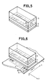
- a sensor produced according to the invention comprises, as shown in FIG. 5, a layer of a semiconductor material 3, carrying on one of its faces, a layer of a ferrimagnetic material 2 and, on the face opposite the first, couples such as 4 of electrodes 41, 42.
- the connections of electrodes 41 and 42 to use circuits such as charge transfer circuits (CCD or Charge Coupled device for example, in English terminology -saxonne), are not shown.
- the assembly is mounted glued to a support part 5 ensuring rigidity and maintenance of the component thus described.
- a ferrimagnetic material such as a Yttrium and Iron garnet (YIG) is grown.
- This growth can be done either by liquid phase epitaxy at a temperature of 980 degrees Celsius at atmospheric pressure, or by vapor phase epitaxy at a temperature between 400 and 700 degrees Celsius under a pressure of 50 to 500 millibars, or finally , by sputtering also designated by "SPUTTERING" in English terminology.
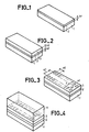
- the thickness h1 of the layer of ferrimagnetic material 2 thus obtained must be approximately 3 microns. A plate is thus obtained as shown in FIG. 1.
- a layer of a semiconductor material 3 is deposited on the previous layer 2 (FIG. 2).
- a semiconductor material consisting of elements of classes 111 and V (or II and Vl) of the periodic table.
- the mesh parameter will be a submultiple of that of the ferrimagnetic material 2 or will have a mesh surface compatible with that of this material.
- This deposition can be done by a vapor phase epitaxy (CVD or Chemical Vapor Deposition in English terminology) and more specifically by vapor phase epitaxy of organometallics designated by MOCVD - (Metalorganic Chemical Vapor Deposition) in English terminology -saxon.
- the epitaxy is done at a temperature between 450 and 700 degrees Celsius under a pressure between 50 millibars and 500 millibars.
- the deposition rate so that the adaptation between the epitaxial material and the layer 2 is done correctly is preferably chosen between 20 Angstroems and 300 Angstroems per minute the thickness h2 of the layer obtained must be between 5 and 10 microns. A plate is thus obtained as shown in FIG. 2.
- metal electrodes such as electrodes 41 and 42 shown in FIG. 3 are deposited on the free surface of layer 3. These electrodes are arranged in pairs such as as 4 for the electrodes 41 and 42. As an exemplary embodiment, these pairs of electrodes have been deposited, as shown in FIG. 3, along a line.
- the distance e1 between two electrodes of the same couple is approximately 10 microns.
- the distance e2 between axes of two pairs of electrodes is between 3 and 5 microns.
- an insulating and rigid substrate 5 is fixed to the surface of the layer 3 carrying the electrodes 41, 42.
- This fixing can be done by any known method such as bonding. A component is thus obtained as shown in FIG. 4.
- the substrate 1 is removed by a process adapted to the nature of the substrate 1 such as mechanical or chemical machining.
- the total removal of the substrate 1 is not compulsory, but the thickness of the substrate possibly remaining should not exceed 0.5 microns.
- the substrate 1 can be a barium and fluorine salt (BaF 2 ).
- the deposition of the layer of ferrimagnetic material is done by sputtering (SPUTTERING). It is also advisable to provide crystallization by annealing after this deposition and before the deposition of the semiconductor material 3.
- the removal of the substrate 1 will then be done by dissolving the salt in a suitable solution.
- Such a sensor can be used as a detector of magnetic information recorded on a magnetic medium.
- This support can be a magnetic strip, a magnetic card, bubble memories, etc.
- a magnetic strip 6 carrying magnetic information 70, 71, 72, etc., arranged along a line such as 7 transverse to the strip 6.
- the strip 6 moves according to arrow F under the sensor described above.
- the information such as 70, 71, 72 are regularly arranged at a pitch equal to the pitch (e2) of the pairs of electrodes.
- the information line 7 passes close to the layer 2 of the sensor, at approximately 2 to 3 microns, each information such as 71 being under a pair of electrodes such as 4.
- Each pair of electrodes is oriented along an OX axis.
- the line of pairs of electrodes is oriented along an OY axis perpendicular to the OX axis.
- An information line 7 is therefore also oriented along the axis OY.
- Information, such as 71, induces a magnetic field which in layer 3, near the pair of electrodes 4, is parallel to the axis OY.
- the YIG layer transfers the magnetic field to the surface of the strip at the level of the semiconductor with a scale factor which depends directly on the magnetization of the garnet. Indeed, at a distance of about the track width, the field value is about 400 G, it would be ten times less if the YIG layer was not present.
- the leakage field of the magnetic domains of the strip is detected.
- MRL Linear Magneto-Resistive
- a charge transfer line - (LTC or CCD) 8 comprising as many cells 80 to 81 as there are pairs of 'electrodes, a cell being coupled to each pair of electrodes.
- FIG. 8 shows several sensors which are combined as described above, which makes it possible to simultaneously read an information matrix arranged on an information medium.
- the sensors thus associated are in fact produced in one piece, which makes it possible to economically manufacture a read head adapted to a specific use.
- a read head has been represented comprising 4 rows of pairs of electrodes (such as 4 and 9), arranged on the same layer of semiconductor material 3, but there may be have a lot more.
- Such an embodiment makes it possible to be adapted to the reading of information bits of approximately 3 microns by 3 microns, that is to say detectable magnetic domains of 10 microns per square of surface.
Landscapes
- Engineering & Computer Science (AREA)
- Physics & Mathematics (AREA)
- Chemical & Material Sciences (AREA)
- Nanotechnology (AREA)
- Condensed Matter Physics & Semiconductors (AREA)
- General Physics & Mathematics (AREA)
- Crystallography & Structural Chemistry (AREA)
- Manufacturing & Machinery (AREA)
- Hall/Mr Elements (AREA)
- Measuring Magnetic Variables (AREA)
Abstract
Description
- L'invention concerne un capteur à effet magnéto résistif, son procédé de réalisation et son application à un détecteur de domaines magnétiques. Un tel détecteur peut être utilisé pour la lecture de supports d'informations magnétiques et permet de lire simultanément un ensemble d'informations.
- Les capteurs utilisant l'effet magnéto résistif linéaire (MRL) sont connus.
- On considère une couche mince de semiconducteur (quelques microns) dans laquelle circule un fort courant. Lorsqu'ils sont soumis à un champ magnétique perpendiculaire au courant dans le plan de la couche, les porteurs (électrons et trous) sont défléchis perpendiculairement à la couche et dans le même sens. L'effet Hall classique suppose que les courants des deux porteurs sont différents. Les forces appliquées aux porteurs majoritaires sont annulées par le champ de Hall. Dans l'effet MRL les courants sont équilibrés, aucun champ ne s'oppose à la déflexion des porteurs qui s'amassent sur l'une des surfaces délimitant la couche. Les vitesses de recombinaison sur chacune de ces surfaces sont choisies très différentes de manière à ce que la concentration moyenne de porteurs dans la couche soit augmentée ou diminuée suivant le sens du champ magnétique. La résistance de la couche au courant injecté varie linéairement avec le champ magnétique.
- Actuellement, cet effet est trop faible pour pouvoir réaliser la lecture d'informations enregistrées sur des supports magnétiques, tels qu'une bande magnétique, dont les bits inscrits développent des champs magnétiques de trop faible valeur. En effet, un champ de fuite de quelques dizaines de Gauss à une distance de 3 αm à 5u.m ne suffit pas à induire un courant suffisant dans la couche de semiconducteur. Il faut un champ de plusieurs centaines de Gauss.
- C'est pourquoi l'invention fournit un capteur permettant d'amplifier et de lire des informations magnétiques donc les champs magnétiques de faibles intensités telles que des informations enregistrées sur bandes magnétiques ou dans des mémoires à bulles magnétiques.
- L'invention concerne donc un capteur à effet magnéto résistif linéaire, caractérisé en ce qu'il comprend : une couche d'un matériau semi-conducteur comportant une première face et une deuxième face ; une couche d'un matériau ferrimagnétique recouvrant la première face de la couche de matériau semi-conducteur ; au moins un couple d'électrodes disposé sur la deuxième face de la couche de matériau semi-conducteur.
- L'invention concerne également un procédé de réalisation d'un capteur à effet magnéto résistif, caractérisé en ce qu'il comporte les différentes phases suivantes :
- a) une première phase de dépôt d'une couche d'un matériau ferrimagnétique sur un premier substrat ;
- b) une deuxième phase de dépôt d'une couche d'un matériau semi-conducteur sur la couche de matériau ferrimagnétique ;
- c) une troisième phase de dépôt d'électrodes sur la couche de matériau semi-conducteur ;
- d) une quatrième phase de fixation du composant obtenu sur un deuxième substrat en matériau isolant par la face portant les électrodes ;
- e) une cinquième phase d'enlèvement de tout ou partie du premier substrat.
- Enfin, l'invention concerne également un détecteur de domaines magnétiques comportant un support magnétique comportant au moins un domaine induisant un champ magnétique selon une première direction déterminée, caractérisé en ce qu'il comporte également un capteur comprenant principalement :
- -une couche d'un matériau semi-conducteur comportant une première et une deuxième face ;
- -une couche d'un matériau ferrimagnétique déposée sur la première face du matériau semi- conducteur ;
- -au moins un couple de deux électrodes disposées sur la deuxième face du matériau semi-conducteur, selon une deuxième direction ; ledit capteur étant disposé de telle façon que sa face portant la couche de matériau ferrimagnétique soit à proximité du support magnétique et que la deuxième direction des deux électrodes soit perpendiculaire à la première direction du champ magnétique.
- Les différents objets et caractéristiques seront détaillés dans la description qui va suivre, faite en se reportant aux figures annexées qui représentent
- -les figures 1 à 5 un exemple de procédé de réalisation d'un capteur à effet magnéto résistif linéaire selon l'invention,
- -la figure 6, un exemple de détecteur selon l'invention ;
- -la figure 7, une variation de réalisation d'un détecteur selon l'invention ;
- -la figure 8, une autre variante de réalisation d'un détecteur selon l'invention.
- Un capteur réalisé selon l'invention comporte, comme cela est représenté en figure 5, une couche d'un matériau semi-conducteur 3, portant sur l'une de ses faces, une couche d'un matériau ferrimagnétique 2 et, sur la face opposée à la première, des couples tels que 4 d'électrodes 41, 42. Les connexions des électrodes 41 et 42 vers des circuits d'utilisation tels que des circuits à transfert de charge (CCD ou Charge Coupled device par exemple, en terminologie anglo-saxonne), ne sont pas représentées. L'ensemble est monté collé sur une pièce support 5 assurant une rigidité et un maintien du composant ainsi décrit.
- En se reportant aux figures 1 à 5, on va maintenant décrire un exemple de procédé de réalisation d'un capteur selon l'invention.
- Au cours d'une première phase, sur un substrat 1 de forme plane réalisé dans du grenat de gadolinium et gallium (GGG) on effectue une croissance d'un matériau ferrimagnétique tel qu'un grenat d'Yttrium et de Fer (YIG).
- Cette croissance peut se faire soit par épitaxie en phase liquide à une température de 980 degrés Celsius à la pression atmosphérique, soit par épitaxie en phase vapeur à une température comprise entre 400 et 700 degrés Celsius sous une pression de 50 à 500 millibars, soit enfin, par pulvérisation cathodique également désignée par "SPUTTERING" en terminologie anglo-saxonne.
- L'épaisseur h1 de la couche de matériau ferrimagnétique 2 ainsi obtenue doit être d'environ 3 microns. On obtient ainsi une plaquette telle que représentée en figure 1.
- Au cours d'une deuxième phase, on réalise un dépôt d'une couche d'un matériau semi-conducteur 3 sur la couche 2 précédente, (figure 2). On choisira un matériau semi-conducteur constitué d'éléments des classes 111 et V (ou Il et Vl) de la classification périodique des éléments. Le paramètre de maille sera un sous-multiple de celui du matériau ferrimagnétique 2 ou présentera une surface de maille compatible avec celle de ce matériau.
- Ce dépôt peut se faire par un procédé d'épitaxie en phase vapeur (CVD ou Chemical Vapor Deposition en terminologie anglo-saxonne) et plus précisément par épitaxie en phase vapeur d'organométalliques désigné par MOCVD - (Metalorganic Chemical Vapor Deposition) en terminologie anglo-saxonne. L'épitaxie se fait à une température comprise entre 450 et 700 degrés Celsius sous une pression comprise entre 50 millibars et 500 millibars. La vitesse de dépôt pour que l'adaptation entre le matériau épitaxié et la couche 2 se fasse correctement est choisie de préférence entre 20 Angstroems et 300 Angstroems par minute l'épaisseur h2 de la couche obtenue doit être comprise entre 5 et 10 microns. On obtient ainsi une plaquette telle que représentée en figure 2.
- Au cours d'une troisième phase on dépose, par tout procédé connu dans la technique, sur la surface libre de la couche 3, des électrodes métalliques telles que les électrodes 41 et 42 représentées sur la figure 3. Ces électrodes sont disposées par couples tel que 4 pour les électrodes 41 et 42. A titre d'exemple de réalisation, ces couples d'électrodes ont été déposées, comme montré sur la figure 3, selon une ligne.
- La distance e1 entre deux électrodes d'un même couple est d'environ 10 microns. La distance e2 entre axes de deux couples d'électrodes est comprise entre 3 et 5 microns.
- Au cours d'une quatrième phase, un substrat isolant et rigide 5 est fixé sur la surface de la couche 3 portant les électrodes 41, 42. Cette fixation peut se faire par tout procédé connu tel qu'un collage. On obtient ainsi un composant tel que représenté en figure 4.
- Au cours d'une cinquième phase, on procède à l'enlèvement du substrat 1 par un procédé adapté à la nature du substrat 1 tel qu'un usinage mécanique ou chimique. L'enlèvement total du substrat 1 n'est pas obligatoire mais il conviendra que l'épaisseur de substrat restant éventuellement n'excède pas 0,5 microns. On obtient alors un capteur tel que représenté en figure 5.
- Il est à noter que l'enlèvement du substrat 1 aurait pu se faire entre la deuxième ou troisième phase ou entre la troisième et la quatrième phase.
- Selon une variante du procédé de réalisation selon l'invention, le substrat 1 peut être un sel de Baryum et de Fluor (BaF2). Dans ce cas, le dépôt de la couche de matériau ferrimagnétique se fait par pulvérisation cathodique (SPUTTERING). Il convient de plus de prévoir une cristallisation par recuit après ce dépôt et avant le dépôt du matériau semi-conducteur 3.
- L'enlèvement du substrat 1 se fera par la suite par dissolution du sel dans une solution adaptée.
- On obtient ainsi comme précédemment un capteur tel que représenté en figure 5.
- Un tel capteur peut être utilisé comme détecteur d'informations magnétiques enregistrées sur un support magnétique. Ce support peut être une bande magnétique, une carte magnétique, des mémoires à bulles, etc. A titre d'exemple, sur la figure 6, une bande magnétique 6 portant des informations magnétiques 70, 71, 72, etc, arrangées selon une ligne telle que 7 transversale à la bande 6.
- La bande 6 se déplace selon la flèche F sous le capteur décrit précédemment. Les informations telles que 70, 71, 72 sont disposées régulièrement selon un pas égal au pas (e2) des couples d'électrodes. Lorsque la bande 6 se déplace, la ligne d'informations 7 passe à proximité de la couche 2 du capteur, à environ 2 à 3 microns, chaque information telle que 71 se trouvant sous un couple d'électrodes tel que 4.
- Chaque couple d'électrodes est orientée selon un axe OX. La ligne de couples d'électrodes est orientée selon un axe OY perpendiculaire à l'axe OX. Une ligne d'informations 7 est .donc orientée également selon l'axe OY. Une information, telle que 71, induit un champ magnétique qui dans la couche 3, à proximité du couple d'électrodes 4, est parallèle à l'axe OY.
- La couche de YIG reporte au niveau du semi- conducteur le champ magnétique à la surface de la bande avec un facteur d'échelle qui dépend directement de l'aimantation du grenat. En effet, à une distance d'environ la largeur de piste, la valeur du champ est d'environ 400 G, elle serait dix fois moindre si la couche de YIG n'était pas présente.
- On peut analyser la reproduction d'un motif aimanté dans un support magnétique par la configuration des domaines dans une couche de grenat. Si on compare les champs de fuite de la bande et du grenat, on met donc en évidence un facteur d'échelle.
- En soumettant la couche de semi-conducteur 3 épitaxiée sur la couche 2 à un champ magnétique par effet MRL (Magnéto Résistif Linéaire) on détecte le champ de fuite des domaines magnétiques de la bande. La forte anisotropie du YIG permet d'augmenter et de canaliser le champ magnétique de fuite des bits à lire.
- Dans le cas d'une application à la lecture d'un support magnétique se déplaçant sous le capteur on aura intérêt, lors de l'enlèvement de la couche 1 de substrat d'en laisser une faible épaisseur (0,5 microns par exemple). Cette couche de substrat jouera le rôle de couche résistante mécanique et protégera la couche ferrimagnétique 2.
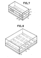
- Selon une variante de réalisation représentée en figure 7, on associe à la ligne de couples d'électrodes 4, une ligne à transfert de charge - (LTC ou CCD) 8 comportant autant de cellules 80 à 81 qu'il y a de couples d'électrodes, une cellule étant couplée à chaque couple d'électrodes. Une telle structure permettra de faciliter la lecture simultanée d'une ligne d'informations.
- Selon une autre variante de réalisation de l'invention, représentée en figure 8, on associe plusieurs capteurs tels que décrits précédemment ce qui permet de lire simultanément une matrice d'informations disposées sur un support d'informations. Selon cet exemple de réalisation, les capteurs ainsi associés sont en fait réalisés en une seule pièce ce qui permet de fabriquer économiquement une tête de lecture adaptée à une utilisation spécifique. C'est ainsi que sur la figure 8, on a représenté une tête de lecture comportant 4 rangées de couples d'électrodes (telles que 4 et 9), disposées sur une même couche de matériau semi-conduteur 3, mais il peut y en avoir beaucoup plus.
- Une telle réalisation permet d'être adaptée à la lecture de bits d'informations d'environ 3 microns sur 3 microns, soit des domaines magnétiques détectables de 10 microns au carré de surface.
Claims (29)
Applications Claiming Priority (2)
| Application Number | Priority Date | Filing Date | Title |
|---|---|---|---|
| FR8508162 | 1985-05-30 | ||
| FR8508162A FR2582862B1 (fr) | 1985-05-30 | 1985-05-30 | Capteur a effet magneto-resistif lineaire, son procede de realisation et son application dans un detecteur de domaines magnetiques |
Publications (2)
| Publication Number | Publication Date |
|---|---|
| EP0206865A1 true EP0206865A1 (fr) | 1986-12-30 |
| EP0206865B1 EP0206865B1 (fr) | 1989-07-26 |
Family
ID=9319702
Family Applications (1)
| Application Number | Title | Priority Date | Filing Date |
|---|---|---|---|
| EP86401117A Expired EP0206865B1 (fr) | 1985-05-30 | 1986-05-27 | Capteur à effet magnéto-résistif linéaire, son procédé de réalisation et son application dans un détecteur de domaines magnétiques |
Country Status (5)
| Country | Link |
|---|---|
| US (1) | US4827218A (fr) |
| EP (1) | EP0206865B1 (fr) |
| JP (1) | JPS61276385A (fr) |
| DE (1) | DE3664703D1 (fr) |
| FR (1) | FR2582862B1 (fr) |
Families Citing this family (21)
| Publication number | Priority date | Publication date | Assignee | Title |
|---|---|---|---|---|
| US4912451A (en) * | 1988-03-28 | 1990-03-27 | Nippon Soken, Inc. | Heterojunction magnetic field sensor |
| US4953590A (en) * | 1988-04-22 | 1990-09-04 | Tokyo Keiki Company Ltd. | Electromagnetic directional control valve |
| US4988850A (en) * | 1988-05-25 | 1991-01-29 | Murata Mfg. Co., Ltd. | Magnetoresistance element array |
| US5057678A (en) * | 1988-06-09 | 1991-10-15 | Hitachi Metals, Ltd. | Magnetic sensor and card reader containing it |
| FR2650106B1 (fr) * | 1989-07-21 | 1991-09-20 | Thomson Csf | Tete magnetique d'enregistrement multipiste a grand contraste de champ |
| JP2522214B2 (ja) * | 1989-10-05 | 1996-08-07 | 日本電装株式会社 | 半導体装置およびその製造方法 |
| US5043693A (en) * | 1990-08-13 | 1991-08-27 | The United States Of America As Represented By The Secretary Of The Navy | Heterogeneous magnetoresistive layer |
| US5134248A (en) * | 1990-08-15 | 1992-07-28 | Advanced Temperature Devices, Inc. | Thin film flexible electrical connector |
| USD329989S (en) | 1991-08-02 | 1992-10-06 | Nu-Metrics, Inc. | Traffic counter |
| DE4425356C2 (de) * | 1993-09-29 | 1998-07-02 | Siemens Ag | Magnetoresistiver Sensor unter Verwendung eines Sensormaterials mit perowskitähnlicher Kristallstruktur |
| FR2723243B1 (fr) * | 1994-07-26 | 1996-09-06 | Thomson Csf | Dispositif d'enregistrement et/ou de lecture de tetes magnetiques et son procede de realisation |
| US5767673A (en) * | 1995-09-14 | 1998-06-16 | Lucent Technologies Inc. | Article comprising a manganite magnetoresistive element and magnetically soft material |
| US5622874A (en) * | 1995-12-14 | 1997-04-22 | Nec Research Institute, Inc. | Process for forming a magnetoresistive sensor for a read/write head |
| US5712612A (en) * | 1996-01-02 | 1998-01-27 | Hewlett-Packard Company | Tunneling ferrimagnetic magnetoresistive sensor |
| US6114188A (en) * | 1996-04-12 | 2000-09-05 | Northeastern University | Method of fabricating an integrated complex-transition metal oxide device |
| US6171886B1 (en) * | 1998-06-30 | 2001-01-09 | Eastman Kodak Company | Method of making integrated hybrid silicon-based micro-actuator devices |
| FR2786345B1 (fr) | 1998-11-24 | 2001-02-09 | Thomson Csf | Dispositif de cryptage quantique |
| DE10016636A1 (de) | 2000-04-04 | 2001-10-18 | Siemens Ag | Stellungsregler, insbesondere für ein durch einen Antrieb betätigbares Ventil |
| US7149173B2 (en) * | 2000-10-17 | 2006-12-12 | Thales | Medium for recording optically readable data, method for making same and optical system reproducing said data |
| FR2824905B1 (fr) * | 2001-05-15 | 2003-08-29 | Thomson Csf | Gyrometre a fibre optique |
| US8018345B2 (en) * | 2005-09-08 | 2011-09-13 | Sri International | RFID tags having ferromagnetic patches |
Citations (1)
| Publication number | Priority date | Publication date | Assignee | Title |
|---|---|---|---|---|
| US3898359A (en) * | 1974-01-15 | 1975-08-05 | Precision Electronic Component | Thin film magneto-resistors and methods of making same |
Family Cites Families (16)
| Publication number | Priority date | Publication date | Assignee | Title |
|---|---|---|---|---|
| US3731123A (en) * | 1968-11-05 | 1973-05-01 | Sony Corp | Magnetic field detecting apparatus |
| US3607390A (en) * | 1969-09-29 | 1971-09-21 | Ibm | Single crystal ferrimagnetic films |
| FR2165206A5 (fr) * | 1971-12-22 | 1973-08-03 | Cii | |
| US3943481A (en) * | 1972-06-10 | 1976-03-09 | Denki Onkyo Co., Ltd. | Galvano-magnetic effect device |
| US4046618A (en) * | 1972-12-29 | 1977-09-06 | International Business Machines Corporation | Method for preparing large single crystal thin films |
| US3909710A (en) * | 1974-01-14 | 1975-09-30 | Us Air Force | Magnetic surface wave rotation rate sensor using the sagnac effect |
| JPS5133898A (fr) * | 1974-09-17 | 1976-03-23 | Hitachi Ltd | |
| JPS51147191A (en) * | 1975-06-12 | 1976-12-17 | Asahi Chem Ind Co Ltd | Hall element and its method of manufacturing |
| US4097802A (en) * | 1975-06-30 | 1978-06-27 | International Business Machines Corporation | Magnetoresistive field sensor with a magnetic shield which prevents sensor response at fields below saturation of the shield |
| US4147584A (en) * | 1977-12-27 | 1979-04-03 | Burroughs Corporation | Method for providing low cost wafers for use as substrates for integrated circuits |
| JPS57177583A (en) * | 1981-04-14 | 1982-11-01 | Int Standard Electric Corp | Holl effect device |
| JPS58130517A (ja) * | 1982-01-29 | 1983-08-04 | Hitachi Ltd | 単結晶薄膜の製造方法 |
| JPS58166781A (ja) * | 1982-03-26 | 1983-10-01 | Pioneer Electronic Corp | 磁電変換素子 |
| CH659896A5 (de) * | 1982-11-22 | 1987-02-27 | Landis & Gyr Ag | Magnetfeldsensor. |
| GB2143038B (en) * | 1983-07-06 | 1987-12-23 | Standard Telephones Cables Ltd | Hall effect device |
| US4624901A (en) * | 1985-04-04 | 1986-11-25 | Rockwell International Corporation | Intermediary layers for epitaxial hexagonal ferrite films |
-
1985
- 1985-05-30 FR FR8508162A patent/FR2582862B1/fr not_active Expired
-
1986
- 1986-05-27 JP JP61122026A patent/JPS61276385A/ja active Pending
- 1986-05-27 EP EP86401117A patent/EP0206865B1/fr not_active Expired
- 1986-05-27 DE DE8686401117T patent/DE3664703D1/de not_active Expired
-
1988
- 1988-01-15 US US07/145,720 patent/US4827218A/en not_active Expired - Fee Related
Patent Citations (1)
| Publication number | Priority date | Publication date | Assignee | Title |
|---|---|---|---|---|
| US3898359A (en) * | 1974-01-15 | 1975-08-05 | Precision Electronic Component | Thin film magneto-resistors and methods of making same |
Non-Patent Citations (2)
| Title |
|---|
| PATENTS ABSTRACTS OF JAPAN, vol. 7, no. 292 (E-219)[1437], 27 décembre 1983; & JP - A - 58 166 781 (PIONEER K.K.) 01-10-1983 * |
| THIN SOLID FILMS, vol. 100, no. 2, février 1983, pages 81-109, Elsevier Sequoia, Lausanne, CH; R.M. MEHRA et al.: "Magnetoresistance in amorphous semiconductors" * |
Also Published As
| Publication number | Publication date |
|---|---|
| DE3664703D1 (en) | 1989-08-31 |
| EP0206865B1 (fr) | 1989-07-26 |
| JPS61276385A (ja) | 1986-12-06 |
| FR2582862A1 (fr) | 1986-12-05 |
| US4827218A (en) | 1989-05-02 |
| FR2582862B1 (fr) | 1987-07-17 |
Similar Documents
| Publication | Publication Date | Title |
|---|---|---|
| EP0206865B1 (fr) | Capteur à effet magnéto-résistif linéaire, son procédé de réalisation et son application dans un détecteur de domaines magnétiques | |
| EP0284495B1 (fr) | Tête magnétique de lecture pour piste de très faible largeur et procédé de fabrication | |
| EP0270404B1 (fr) | Arrangement de pôles magnétiques, application à une tête magnétique d'enregistrement/lecture et procédé de réalisation | |
| EP0418372A1 (fr) | Tete magnetique de lecture a magnetoresistance pour enregistrement perpendiculaire et procede de realisation d'une telle tete. | |
| EP0107589B1 (fr) | Dispositif d'écriture d'informations sur un support magnétique | |
| EP0779632A1 (fr) | Structure et capteur multicouches et procédé de réalisation | |
| US4623867A (en) | Permanent magnet biased narrow track magnetoresistive transducer | |
| US6117690A (en) | Method of making thin, horizontal-plane hall sensors for read-heads in magnetic recording | |
| EP0214878A1 (fr) | Support d'enregistrement perpendiculaire magnétiquement anisotrope | |
| US6048632A (en) | Self-biasing, non-magnetic, giant magnetoresistance sensor | |
| EP0616484A1 (fr) | Transducteur magnétorésistif et procédé de réalisation | |
| FR2700633A1 (fr) | Procédé de réalisation d'une tête magnétique à détecteur de champ à semiconducteur et tête obtenue par ce procédé. | |
| EP0642030B1 (fr) | Guide de flux magnétique à languettes et capteur magnétorésistif comportant ce guide | |
| EP0012649A1 (fr) | Tête de lecture magnétique | |
| EP0443941A1 (fr) | Tête magnétique horizontale à effet hall et son procédé de réalisation | |
| EP0046697A1 (fr) | Transducteur magnétique intégré | |
| EP1055132A1 (fr) | Capteur de champ magnetique a magnetoresistance geante | |
| EP0642181A1 (fr) | Composant et capteur magnétorésistifs à motif géométrique répété | |
| EP0406051A1 (fr) | Tête de lecture magnétique à effet hall | |
| FR2671220A1 (fr) | Procede de fabrication de capteurs magneto-resistifs, et dispositif magnetique realise suivant un tel procede. | |
| US5622874A (en) | Process for forming a magnetoresistive sensor for a read/write head | |
| FR2898414A1 (fr) | Composant sensible a un champ magnetique comportant un semi-conducteur magnetique dilue, dispositifs l'incorporant et procede de mise en oeuvre. | |
| FR2622336A1 (fr) | Tete magnetique de lecture et d'enregistrement | |
| EP0658772A1 (fr) | Capteur magnétique à effet magnéto-résistif | |
| WO2007090946A1 (fr) | Semi-conducteur ferromagnetique, son procede de fabrication, composants l'incorporant et utilisations de ce semi-conducteur s'y rapportant |
Legal Events
| Date | Code | Title | Description |
|---|---|---|---|
| PUAI | Public reference made under article 153(3) epc to a published international application that has entered the european phase |
Free format text: ORIGINAL CODE: 0009012 |
|
| AK | Designated contracting states |
Kind code of ref document: A1 Designated state(s): DE GB IT NL |
|
| 17P | Request for examination filed |
Effective date: 19870126 |
|
| 17Q | First examination report despatched |
Effective date: 19880915 |
|
| RAP3 | Party data changed (applicant data changed or rights of an application transferred) |
Owner name: THOMSON-CSF |
|
| GRAA | (expected) grant |
Free format text: ORIGINAL CODE: 0009210 |
|
| AK | Designated contracting states |
Kind code of ref document: B1 Designated state(s): DE GB IT NL |
|
| ITF | It: translation for a ep patent filed | ||
| REF | Corresponds to: |
Ref document number: 3664703 Country of ref document: DE Date of ref document: 19890831 |
|
| GBT | Gb: translation of ep patent filed (gb section 77(6)(a)/1977) | ||
| PLBE | No opposition filed within time limit |
Free format text: ORIGINAL CODE: 0009261 |
|
| STAA | Information on the status of an ep patent application or granted ep patent |
Free format text: STATUS: NO OPPOSITION FILED WITHIN TIME LIMIT |
|
| 26N | No opposition filed | ||
| PGFP | Annual fee paid to national office [announced via postgrant information from national office to epo] |
Ref country code: DE Payment date: 19910419 Year of fee payment: 6 |
|
| PGFP | Annual fee paid to national office [announced via postgrant information from national office to epo] |
Ref country code: GB Payment date: 19910423 Year of fee payment: 6 |
|
| ITTA | It: last paid annual fee | ||
| PGFP | Annual fee paid to national office [announced via postgrant information from national office to epo] |
Ref country code: NL Payment date: 19910531 Year of fee payment: 6 |
|
| PG25 | Lapsed in a contracting state [announced via postgrant information from national office to epo] |
Ref country code: GB Effective date: 19920527 |
|
| PG25 | Lapsed in a contracting state [announced via postgrant information from national office to epo] |
Ref country code: NL Effective date: 19921201 |
|
| NLV4 | Nl: lapsed or anulled due to non-payment of the annual fee | ||
| GBPC | Gb: european patent ceased through non-payment of renewal fee |
Effective date: 19920527 |
|
| PG25 | Lapsed in a contracting state [announced via postgrant information from national office to epo] |
Ref country code: DE Effective date: 19930202 |
|
| PG25 | Lapsed in a contracting state [announced via postgrant information from national office to epo] |
Ref country code: IT Free format text: LAPSE BECAUSE OF NON-PAYMENT OF DUE FEES;WARNING: LAPSES OF ITALIAN PATENTS WITH EFFECTIVE DATE BEFORE 2007 MAY HAVE OCCURRED AT ANY TIME BEFORE 2007. THE CORRECT EFFECTIVE DATE MAY BE DIFFERENT FROM THE ONE RECORDED. Effective date: 20050527 |