EP0206892A1 - Verarbeitungsverfahren für ein ursprüngliches Bild darstellende digitale Signale - Google Patents
Verarbeitungsverfahren für ein ursprüngliches Bild darstellende digitale Signale Download PDFInfo
- Publication number
- EP0206892A1 EP0206892A1 EP86401215A EP86401215A EP0206892A1 EP 0206892 A1 EP0206892 A1 EP 0206892A1 EP 86401215 A EP86401215 A EP 86401215A EP 86401215 A EP86401215 A EP 86401215A EP 0206892 A1 EP0206892 A1 EP 0206892A1
- Authority
- EP
- European Patent Office
- Prior art keywords
- module
- pixels
- binary elements
- pixel
- image
- Prior art date
- Legal status (The legal status is an assumption and is not a legal conclusion. Google has not performed a legal analysis and makes no representation as to the accuracy of the status listed.)
- Granted
Links
Images


Classifications
-
- G—PHYSICS
- G06—COMPUTING OR CALCULATING; COUNTING
- G06F—ELECTRIC DIGITAL DATA PROCESSING
- G06F17/00—Digital computing or data processing equipment or methods, specially adapted for specific functions
- G06F17/10—Complex mathematical operations
- G06F17/15—Correlation function computation including computation of convolution operations
- G06F17/153—Multidimensional correlation or convolution
-
- G—PHYSICS
- G06—COMPUTING OR CALCULATING; COUNTING
- G06T—IMAGE DATA PROCESSING OR GENERATION, IN GENERAL
- G06T5/00—Image enhancement or restoration
- G06T5/20—Image enhancement or restoration using local operators
Definitions
- the present invention relates to a method for processing digitized signals representative of an original image, and in particular of an image defined by scanning lines, such as an image produced from video signals for example.
- This invention applies to the restoration and improvement of the contrasts of video-type images, to the detection of outlines and to the structuring of images.
- each pixel aq of the original image to be processed is defined by its intensity a in the form of E binary elements, and its coordinates i and j, i being the number of a scanning line considered of this original image and j being the number of the pixel on this scan line.
- the original image is processed by convolution, by a convolution window of dimensions L X P which includes L lines of P coefficients.
- Each of these weighting coefficients C l, k is defined by its value C and its coordinates I and k inside the window.
- Each window is centered on the corresponding pixel a ij .
- the processing module provides for each pixel a i, j of the original image, a pixel b i, j of a convoluted image, defined by its intensity b, in the form of G binary elements and its coordinates i and j.
- the pixel b ij is obtained from successive sums of products defined by the relation:
- a known convolution processing module is for example described in the journal Computer Vision, Graphies and image processing, vol. 27, pages 115-123 (1984).
- a module of this type is also described in the IEEE acts, in an article entitled "large Array VLSI fiiter", volume 83-CH 1929-9 (1983), pages 15 to 21.
- the processing of the pixels of an image whose characteristics do not correspond to those of the pixels of the image to be processed is impossible, even using complicated circuits associated with this module. It follows that for an image having predetermined characteristics (number of pixels per line, number of binary elements defining each pixel, dimensions of the convolution window), it is necessary to build a specific module, taking into account the characteristics of this original image to be processed to obtain a convoluted image. It is the same when changing application and it is necessary to modify the coefficients of the convolution window.
- the invention aims to remedy these drawbacks and in particular to provide a method for processing digital signals, representative of an original image defined by scanning lines, without having to design a specific module.
- This method allows, by association of basic modules allowing each to process a basic image having predetermined characteristics (number of pixels per line, number of binary elements per pixel, dimensions of the predetermined convolution window), to process an image origin, regardless of the number of pixels in each line of this image, or regardless of the number of binary elements defining each pixel of this image, or whatever the dimensions of the convolution window defined for the processing of each pixel of this original image, or whatever the values of the coefficients of the convolution window.
- it consists in interconnecting n basic modules in series so that the processed data output of a module is connected to a processed data input of a next module, the H binary elements of each pixel of l the original image being separated into n groups of E binary elements, each module receiving on its data input to be processed a corresponding group of E binary elements, the processed data output of the last module in the series providing the binary elements of each pixel of the convoluted image.
- the method in the case where the dimensions L'xP 'of a window chosen to process each pixel of the original image are greater than the dimensions LX P of the processing window of the basic module, it consists in interconnecting r x s basic modules in r rows and s columns, such that the S modules of the first row receive the binary elements of each pixel of S groups of N + P-1 pixels of the original image, each group being shifted by P pixels with respect to the previous one, and that the r-1 modules of each of the columns receive the binary elements of pixels already processed in the previous module of the same column, the method then consisting in interconnecting available adders in each module so as to sum the partial convolution results provided by each module on a serial output - (SSPL), this summation of rx S partial results being performed in series in adders with two inputs.
- SSPL serial output -
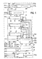
- FIG. 1 shows in detail one of the basic modules used in the processing method of the invention.
- This basic module is capable of processing an image comprising N pixels per scanning line, each pixel being defined by a number E of binary elements representing a quantity coded in addition to 2 and the convolution processing being carried out in a window of dimensions.
- LX P centered on the pixel being processed.
- This module can be qualified as a basic module since, as will be seen below in detail, the original image whose pixels are to be treated has different characteristics: this original image can have a number of pixels per scanning line, which is a multiple of the number of pixels N that the basic module can process; in this original image, each pixel can be defined by a number of binary elements which is multiple of the number of binary elements E defining each pixel which the basic module can process; finally, each pixel of the original image can also be processed by a convolution window whose dimensions L'xP 'are greater than the dimensions L X P of the window which the basic module can process.
- the convolution window has, for the basic module B of FIG. 1, dimensions L, P (L being the number of lines in the window and P the number of coefficients of each line in this window).
- This basic module B comprises a shift buffer register 1 with a capacity of (N + P-1) xE binary elements (eb or bits), which receives on an input 2 called EPDO, the E data bits relating to all the pixels of a scanning line, comprising N pixels of E bits each.
- This register has a capacity of (N + P-1) x E bits to take account of the "edge effects" that are encountered in an image of N pixels per line, when the window chosen has a width of P pixels.
- the shift register 1 also receives on another validation input 3, an EVAL signal and on a clock input 4, a clock signal HDON.
- the clock signal makes it possible to record the E bits of new data present on the EPDO input and to shift the data already acquired in register 1 by one position.
- the clock signal HDON is active only if the EVAL signal is brought to the logical value "1".
- the convolution operator 20 has an output 27 providing bits representative of data. SPRE coded on G bits, and corresponding to the pixels of the convoluted image.
- This convolution operator also includes outputs 28 and 29.
- Output 28 provides SSEE data corresponding to partial convolution results, in the case where the image to be processed comprises N pixels per line, each pixel being defined by a number of bit which is a multiple of the number E of bits defining each pixel of the base image.
- the serial output 29 provides relative SSPL data of the partial convolution results, in the case where the image to be processed comprises N pixels of E bits per scanning line, but in which the chosen convolution window has dimensions which are respectively greater the dimensions of the convolution window in which the basic module performs the processing.
- the convolution operator 20 also includes a serial input 30 receiving ESEE data representative of partial convolution results coming from the SSEE output of another basic module, in the case where the image to be processed comprises N pixels per line of scanning, but in which each pixel is defined by a number of bits which is a multiple of the number of bits E of each pixel which the basic module can process.
- the control circuit 24 receives control signals DE / DS and SYLI respectively on its inputs 37 and 26, and a clocked signal HORL on input 32, as well as the signal INI making it possible to initialize the entire module basic. From these signals, the control circuit 24 supplies a clock signal HCAL internal to the module, intended to sequence the processing necessary for obtaining N pixels of the convoluted image. In addition, the control circuit 24 provides the necessary signals (not shown in FIG.
- the basic module which has just been described further comprises, according to the invention, a first secondary shift register 33 with a capacity of P bits receiving on inputs 34, 35 the clock signals HDON, as well as the validation signal EVAL A serial output of this shift register is connected to a serial input of a second secondary shift register 36 with a capacity of (NP) bits, this second register receives on another input the clock signal HDON.
- the first register 35 provides on its output, a SVAP signal making it possible to validate, as will be seen below, the recording of the data in another module identical to the basic module, in the case where the convolution window chosen to process the 'original image has dimensions L', P 'which are respectively greater than the dimensions L, P of the processing window of the basic module.
- an SVAP signal is supplied as soon as the number of pixels recorded in this module exceeds the number P of pixels defining the processing window of the basic module.
- the second register 36 provides an SVAN signal on a serial output.
- This SVAN signal makes it possible to validate the recording of data in another module identical to the basic module when the number of pixels per line of the original image is a multiple of the number N of pixels per line which the basic module.
- this signal is supplied by a basic module as soon as the number of pixels recorded in the module exceeds the number N of pixels that the basic module can process.
- the basic module is provided with a serial adder 38 receiving the HCAL signal from the internal processing clock, supplied by the control module 24.
- This 1-bit serial adder adds a bit occurring on input 39 called ESPL1 with either a bit occurring at the same time on input 40 called ESPL2 if the RETA signal, applied to input 41, is brought to the logic state "0", or a bit presented on input 40, an HCAL clock period earlier if the RETA signal is brought to the logic state "1".
- the result bit is then presented on output 42 called SSPLR.
- This adder is used, in the method of the invention, in the case where the convolution window chosen to process the original image has dimensions L 'and P' respectively greater than the dimensions L and P of the module processing window basic, as we will see in detail below.
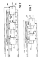
- the H binary elements coding in complement to two each pixel of the original image are separated into N groups of E binary elements.
- Each module receives on its EPDO input a corresponding group of E binary elements.
- the input 47 of the module 51 receives the E most significant binary elements.
- the input 48 of the module 52 receives the E binary elements of medium weight, while the input 49 of the module 53 receives E binary elements of low weight.
- the representative data of each pixel is referenced EPDO in the figure.
- the E most significant bits of the EPDO data processed in the module 51 are supposed to encode a signed number, and the signal 0 / DS of this module is fixed in the logic state "0".
- the middle and low weight E bits of data processed in modules 52 and 53 respectively are assumed to code unsigned numbers and the signal DE / DS of these modules is fixed in logic state "1".
- the SSEE output of processed data of a module is linked to an ESEE of processed data of the next module.
- the output 43 of the first module 51 is connected to the input 44 of the second module 52, and that the output 45 of the module 52 is connected to the input 46 of the module 53.
- the SPRE data relating to each pixel of the convoluted image is supplied in the form of G binary elements on the output 50 of the last module 53.
- Each of the modules also receives the signals EVAL, HDON, HORL, INI and SYLI described above, thus than the HCOE and ENCO signals.
- the method of the invention consists in cascading several identical modules to the basic modules, to perform partial convolution treatments, then to add the results of these partial treatments taking into account that the partial results are represented with different weights.
- the method here consists in locating from rank 1 to rank q, each group of N pixels of the original image and to interconnect q basic modules identified from rank 1 to rank q.
- the module of rank 1 For each line of the original image, the module of rank 1 receives the binary elements of each pixel of the group of N pixels of rank 1 as well as the binary elements of the previous pixels and of the following pixels, of this line, and so on up to the module of rank q which receives the binary elements of the group of N pixels, of rank q.
- Ch that module provides on its SPRE output of processed data, N pixels corresponding to each of the groups of ranks 1 to q of each line of the convoluted image.
- the method here consists in using two identical basic modules 60, 61.
- the two modules receive the EPDO data relating to the pixels of each line. These modules also receive HDON, HORL, INI and SYLI signals, as well as DE / DS.
- the first module thanks to the EVAL signal applied to its input 62, processes the first N pixels of each line;
- the second module 61 thanks to an EVAL signal applied to its input 63 coming from the validation output SVAN of the first module 60, processes the following N pixels of each line.
- Each module also receives the ENCO and HCOE signals.
- the first module provides SPRE processed data on an output 65. These data relate to the first N pixels of each line of the convoluted image; SPRE data is coded on G binary elements.
- the second module 61 provides at its output 64 the SPRE data relating to the following N pixels of each line of the convoluted image.
- FIGS. 4A, 4B, 4C schematically represent an interconnection of modules identical to the basic modules, in the case where the dimensions L'xP 'of the window, chosen to process each pixel of the original image, are respectively greater than the dimensions LxP of the processing window of the basic module.
- the method here consists of interconnecting rxs basic modules along r rows R ,, R 2 , R3 and s columns C ,, C z , C3, so that the S modules of the first row R, receive the binary elements of each pixel of S groups of N + P-1 pixels from the original image, each group being shifted by P pixels compared to the previous one, and that the r-1 modules of the same column, from the second row R2 to the last row R 3 , receive the pixel bits already processed in the previous module of this same column.
- the 3 modules 101, 102, 103 of the first row R receive on the input EPDO the E binary elements of the pixels of each of the lines, as well as the clock signal HDON.
- the recording of the data in the module 101 is validated by the appearance of the signal EVAL on the input 100 of this module.
- the EVAL signal is maintained until the bits of the N + P-1 pixels of each of the lines are recorded.
- the module 101 generates on its output 110 called SVAP, a signal corresponding to the previous EVAL signal delayed by P clock periods of the HDON signal, the output 110 of the module 101 is connected to the input 120, also called EVAL, of the following module 102.
- This signal therefore makes it possible to record in the module 102, the binary elements of a group of N + P-1 pixels shifted by P pixels with respect to the group recorded in the module 101.
- module 102 In the same way the module 102 generates on its output 130 called SVAP, a signal corresponding to the signal present on input 120, delayed by P clock periods of the HDON signal, output 130 of module 2, is connected to input 140, called EVAL, of module 3.
- This signal therefore makes it possible to record in the module 103, the binary elements of a group of N + P- 1 pixels shifted by P pixels with respect to the group recorded in the module 102.
- the modules 104, 105, 106, 107, 108, 109 of the following rows R 2 , R , do not receive the EPDO and HDON signals.
- the HDON input of these modules is maintained at logic level "0", thus enabling the ESDO serial input of these modules to be validated.
- the output 150, called SSDO, of the module 101 is connected to the input 160, called ESDO, of the module 104, next module of the first column C ,.
- the output 170 of the module 104 is connected to the input 180 of the next module 107 of this same column C 1
- the same connections are made between the modules 102, 105, and 108 of the second column C z , and between the modules 103, 106 and 109 of the third column C 3 .
- the binary elements of the pixels recorded in the module 101 are presented in series on the output 150 of this module, at the rate of the calculation clock HCAL, after having undergone a delay of L lines, ie L (N + P-1 ) E clock periods of the HCAL signal. These binary elements are then recorded at the same rate, in the module 104, at the level of the first shift register 6 of FIG. 1. It is the same for the passage from the module 104 to the module 107. The same reasoning applies for each of the other columns. All these modules receive the INI, HORL, DE / DS and SYLI signals. They also receive all the binary elements of the coefficients on the ENCO input.
- Each of the modules 101 to 109 provides on its output called SSPL, a convolution series result corresponding to the window portion processed by each of these modules.
- the following interconnections consist in carrying out the sum of all these partial results in four phases, in order to obtain a final result supplied, in the example, by the module 109, on the output 190 called SPRE and providing G bits.
- the SSPL outputs of the modules 101 109 respectively marked from 200 to 208 are connected 2 to 2 to the inputs of serial adders available in each of the modules.
- the output 200 of the module 101 is connected to the input 209, called ESPL1, of this same module and the output 203 of the module 104 is connected to the input 300, called ESPL2 of the module 101.
- the output 201 of the module 102 and the output 204 of the module 105 are respectively connected to the inputs 301 and 302 of the module 102; the output 202 of the module 103 and the output 205 of the module 106 are respectively connected to the inputs 303 and 304 of the module 103; the output 206 of the module 107 and the output 208 of the module 109 are respectively connected to the inputs 305 and 306 of the module 107.
- the output 207 of the module 108 is connected to the input 307 called ESPL2, of the module 105.
- the adders of the modules 101 , 102, 103 and 107 each have their two inputs connected to outputs providing binary elements of the same weight; consequently, for these modules, the RETA signal is fixed at logic level "0", each of the adders performs the sum of two binary elements of the same weight and provides the result of the same weight on the SSPLR output after a clock period of the HCAL signal
- the RETA signal from module 105 is fixed at logic level "1" to delay by a clock period the binary element of the ESPL2 input which is added a binary element coming from the output 309 of the module 102, output SSPLR of the adder of this module, which was itself delayed by this adder.
- the adder of module 105 is used for the second phase of summation of the partial results as well as the adder of module 104 whose inputs 400 and 401 are respectively connected to outputs 402 and 403 of the adder of modules 101 and 107 and whose RETA signal is fixed at logic level "0".
- the signal RETA of this module is fixed at logic level "1" for the same reason as that described above. above for the module 105.
- the adder of the module 106 performs the third phase of summation between the binary elements of its input 405, delayed, and the binary elements of its input 406 connected to the output 407 of the module 105.
- the output 408 of the module 104 is connected to the input 409, called ESPL2, of the module 109.
- the RETA signal of this module is fixed at logic level "1" for the same reason as that described above for the module 105.
- the adder of the module 109 performs the fourth phase of the summation of the partial results between the binary elements of its input 409, delayed, and the binary elements of its input 500, connected to the output 501 of the module 106.
- the results of the N pixels of each line are then available on output 190 of the module 109 in the form of G bits.
- the first phase consists in adding 2 to 2 the results provided by the modules 101 and 104, 102 and 105, 103 and 106, and 107 and 109.
- the second phase consists in adding on the one hand in module 105 the result provided by module 108, delayed, with the result provided by the adder of module 102 and d on the other hand in module 104 the results provided by the adders of modules 101 and 107.
- the third phase consists in adding in module 106 the result provided by the adder of module 103, delayed, with the result provided by the adder of the module 105.
- the fourth phase consists in adding in module 109 the result provided by the adder of module 104, delayed, with the result provided by the adder of module 106.
- the s modules of the first row receive the binary elements of each pixel of a group of N pixels of the original image, as well as the binary elements of the previous pixels and following pixels, corresponding to an elementary window of p pixels per line; the r-1 modules in the same column receive the binary elements of the previous module in the same column (after a delay corresponding to L rows) as the processing proceeds.
- the process consists, here, starting from an original image of N pixels per line marked from 1 to N, to cut each line into s groups of N + P-1 pixels, each group is shifted by P pixels compared to the previous one .
- the group of rank 1 includes the N + P-1 pixels identified by the rank 2 group includes the N + p-1 reixed oixels from and so on up to the group of ranks s which includes the N + P-1 pixels identified by
Landscapes
- Engineering & Computer Science (AREA)
- Physics & Mathematics (AREA)
- General Physics & Mathematics (AREA)
- Theoretical Computer Science (AREA)
- Mathematical Physics (AREA)
- Computational Mathematics (AREA)
- Mathematical Analysis (AREA)
- Mathematical Optimization (AREA)
- Pure & Applied Mathematics (AREA)
- Data Mining & Analysis (AREA)
- Algebra (AREA)
- Databases & Information Systems (AREA)
- Software Systems (AREA)
- General Engineering & Computer Science (AREA)
- Computing Systems (AREA)
- Image Processing (AREA)
Applications Claiming Priority (2)
| Application Number | Priority Date | Filing Date | Title |
|---|---|---|---|
| FR8508739A FR2583184B1 (fr) | 1985-06-10 | 1985-06-10 | Procede de traitement de signaux numerises representatifs d'une image origine |
| FR8508739 | 1985-06-10 |
Publications (2)
| Publication Number | Publication Date |
|---|---|
| EP0206892A1 true EP0206892A1 (de) | 1986-12-30 |
| EP0206892B1 EP0206892B1 (de) | 1991-12-11 |
Family
ID=9320052
Family Applications (1)
| Application Number | Title | Priority Date | Filing Date |
|---|---|---|---|
| EP86401215A Expired - Lifetime EP0206892B1 (de) | 1985-06-10 | 1986-06-05 | Verarbeitungsverfahren für ein ursprüngliches Bild darstellende digitale Signale |
Country Status (5)
| Country | Link |
|---|---|
| US (1) | US4736440A (de) |
| EP (1) | EP0206892B1 (de) |
| JP (1) | JPS61283971A (de) |
| DE (1) | DE3682832D1 (de) |
| FR (1) | FR2583184B1 (de) |
Cited By (5)
| Publication number | Priority date | Publication date | Assignee | Title |
|---|---|---|---|---|
| WO1988007722A3 (en) * | 1987-03-28 | 1988-10-20 | Stonefield Systems Plc | Improvements in or relating to cellular array processing devices |
| EP0288132A3 (en) * | 1987-04-22 | 1990-01-31 | Tektronix, Inc. | System for digitizing the trajectory of a target point of a moving beam |
| FR2636194A1 (fr) * | 1988-09-05 | 1990-03-09 | Commissariat Energie Atomique | Procede de traitement de signaux numerises representatifs d'une image origine |
| FR2638871A1 (fr) * | 1988-11-09 | 1990-05-11 | Jutand Francis | Procede et circuit de filtrage de signal de representation d'image |
| US6237079B1 (en) * | 1997-03-30 | 2001-05-22 | Canon Kabushiki Kaisha | Coprocessor interface having pending instructions queue and clean-up queue and dynamically allocating memory |
Families Citing this family (8)
| Publication number | Priority date | Publication date | Assignee | Title |
|---|---|---|---|---|
| US6336180B1 (en) | 1997-04-30 | 2002-01-01 | Canon Kabushiki Kaisha | Method, apparatus and system for managing virtual memory with virtual-physical mapping |
| US5027419A (en) * | 1989-03-31 | 1991-06-25 | Atomic Energy Of Canada Limited | Optical images by quadrupole convolution |
| AUPO647997A0 (en) | 1997-04-30 | 1997-05-22 | Canon Information Systems Research Australia Pty Ltd | Memory controller architecture |
| US6061749A (en) | 1997-04-30 | 2000-05-09 | Canon Kabushiki Kaisha | Transformation of a first dataword received from a FIFO into an input register and subsequent dataword from the FIFO into a normalized output dataword |
| US6246396B1 (en) | 1997-04-30 | 2001-06-12 | Canon Kabushiki Kaisha | Cached color conversion method and apparatus |
| US6707463B1 (en) | 1997-04-30 | 2004-03-16 | Canon Kabushiki Kaisha | Data normalization technique |
| US6289138B1 (en) | 1997-04-30 | 2001-09-11 | Canon Kabushiki Kaisha | General image processor |
| US6414687B1 (en) | 1997-04-30 | 2002-07-02 | Canon Kabushiki Kaisha | Register setting-micro programming system |
Family Cites Families (3)
| Publication number | Priority date | Publication date | Assignee | Title |
|---|---|---|---|---|
| US4174514A (en) * | 1976-11-15 | 1979-11-13 | Environmental Research Institute Of Michigan | Parallel partitioned serial neighborhood processors |
| JPS6053349B2 (ja) * | 1981-06-19 | 1985-11-25 | 株式会社日立製作所 | 画像処理プロセツサ |
| US4542527A (en) * | 1982-05-17 | 1985-09-17 | Tokyo Shibaura Denki Kabushiki Kaisha | Image processing device for continuously extracting features of small regions of an image |
-
1985
- 1985-06-10 FR FR8508739A patent/FR2583184B1/fr not_active Expired
-
1986
- 1986-06-05 JP JP61131075A patent/JPS61283971A/ja active Pending
- 1986-06-05 DE DE8686401215T patent/DE3682832D1/de not_active Expired - Lifetime
- 1986-06-05 EP EP86401215A patent/EP0206892B1/de not_active Expired - Lifetime
- 1986-06-09 US US06/872,177 patent/US4736440A/en not_active Expired - Fee Related
Non-Patent Citations (2)
| Title |
|---|
| 1981 IEEE COMPUTER SOCIETY WORKSHOP ON COMPUTER ARCHITECTURE FOR PATTERN ANALYSIS AND IMAGE DATABASE MANAGEMENT, Hot Springs, Virginia, US, 11-13 novembre 1981, pages 159,160, Computer Society Press, New York, US; H.T. KUNG et al.: "A systolic 2-D convolution chip" * |
| ICASSP 81 PROCEEDINGS, 30,31 mars - 1 avril 1981, Atlanta, Georgia, US, vol. 2 des 3, pages 658-661, IEEE International Conference on Acoustics, Speech and Signal Processing, New York, US; S.A. WHITE: "Architecture for a digital programmable image processing element" * |
Cited By (7)
| Publication number | Priority date | Publication date | Assignee | Title |
|---|---|---|---|---|
| WO1988007722A3 (en) * | 1987-03-28 | 1988-10-20 | Stonefield Systems Plc | Improvements in or relating to cellular array processing devices |
| EP0288132A3 (en) * | 1987-04-22 | 1990-01-31 | Tektronix, Inc. | System for digitizing the trajectory of a target point of a moving beam |
| FR2636194A1 (fr) * | 1988-09-05 | 1990-03-09 | Commissariat Energie Atomique | Procede de traitement de signaux numerises representatifs d'une image origine |
| EP0358553A1 (de) * | 1988-09-05 | 1990-03-14 | Commissariat A L'energie Atomique | Verfahren zur Verarbeitung von digitalen Bildsignalen |
| FR2638871A1 (fr) * | 1988-11-09 | 1990-05-11 | Jutand Francis | Procede et circuit de filtrage de signal de representation d'image |
| EP0368731A1 (de) * | 1988-11-09 | 1990-05-16 | France Telecom | Verfahren und Anordnung zur Filterung des Bilddarstellungssignals |
| US6237079B1 (en) * | 1997-03-30 | 2001-05-22 | Canon Kabushiki Kaisha | Coprocessor interface having pending instructions queue and clean-up queue and dynamically allocating memory |
Also Published As
| Publication number | Publication date |
|---|---|
| FR2583184B1 (fr) | 1989-06-02 |
| DE3682832D1 (de) | 1992-01-23 |
| EP0206892B1 (de) | 1991-12-11 |
| JPS61283971A (ja) | 1986-12-13 |
| US4736440A (en) | 1988-04-05 |
| FR2583184A1 (fr) | 1986-12-12 |
Similar Documents
| Publication | Publication Date | Title |
|---|---|---|
| EP0206892B1 (de) | Verarbeitungsverfahren für ein ursprüngliches Bild darstellende digitale Signale | |
| EP0198729B1 (de) | System zur Simulation einer elektronischen Schaltung | |
| EP0368731B1 (de) | Verfahren und Anordnung zur Filterung des Bilddarstellungssignals | |
| EP0552074A1 (de) | Mehrfachprozessor-Datenverarbeitungssystem | |
| BE897441A (fr) | Calculateur associatif permettant une multiplication rapide | |
| FR2588142A1 (fr) | Systeme permettant le traitement a haute vitesse par convolutions de donnees d'image. | |
| EP0437876B1 (de) | Programmierbarer serieller Multiplikator | |
| FR2604270A1 (fr) | Additionneur binaire comportant un operande fixe, et multiplieur binaire parallele-serie comprenant un tel additionneur | |
| EP0924627B1 (de) | Pipelineprozessor für die schnelle Fourier-Transformation | |
| EP0237382B1 (de) | Gerät zur Kosinustransformation eines abgetasteten digitalen Signals | |
| EP0667969A1 (de) | ELEKTRONISCHE BERECHNUNGSEINRICHTUNG FüR DIE FOURIER TRANSFORMATION UND VERFAHREN ZUR MINIMISIERUNG DER INTERNEN DATENWEGE DIESER VORRICHTUNG | |
| EP0242258B1 (de) | Vorrichtung zur Durchführung eines Algorithmus (Leroux-Gueguen) zum Codieren eines Signals durch Linearvorhersage | |
| EP0476592A2 (de) | Adressengenerator für den Datenspeicher eines Prozessors | |
| EP0183610B1 (de) | Schreib-Lese-Speicher und Anwendung in einer linearen Interpolationsschaltung | |
| FR2772951A1 (fr) | Procede de commande d'un etage radix 4 d'un dispositif electroonique de calcul d'une transformee de fourier a architecture dite "pipelinee", et dispositif correspondant | |
| EP0190514B1 (de) | On-line-Testeinrichtung für einen Rechnerkreis der diskreten Fouriertransformation und Kreis der eine solche Einrichtung enthält | |
| EP1038236B1 (de) | Verfahren zur berechnung der schnellen fourier-transformation und der schnellen invers-fourier-transformation | |
| EP0175623A1 (de) | Einrichtung zur Echtzeitdigitalsignalverarbeitung durch Faltung | |
| EP0327445A1 (de) | Allgemeiner digitaler Multiplizierer und digitaler Filter mit diesem Multiplizierer | |
| FR2563349A1 (fr) | Multiplieur matriciel systolique de traitement de donnees numeriques | |
| EP0140718B1 (de) | Zelle und Berechnungsschaltung in systolischer Architektur mit derartigen Zellen | |
| CA2359198C (fr) | Unite de calcul pour l'execution d'un protocole cryptographique | |
| FR3161778A1 (fr) | Réseau de neurones binaires | |
| EP0432008A1 (de) | Elektronisches Neuronalnetzwerk und Lernverfahren | |
| EP0125156B1 (de) | Kaskadierter Multiplizierer mit einer Anordnung von elementären Operatoren |
Legal Events
| Date | Code | Title | Description |
|---|---|---|---|
| PUAI | Public reference made under article 153(3) epc to a published international application that has entered the european phase |
Free format text: ORIGINAL CODE: 0009012 |
|
| AK | Designated contracting states |
Kind code of ref document: A1 Designated state(s): DE GB NL |
|
| 17P | Request for examination filed |
Effective date: 19870603 |
|
| RAP1 | Party data changed (applicant data changed or rights of an application transferred) |
Owner name: COMMISSARIAT A L'ENERGIE ATOMIQUE |
|
| 17Q | First examination report despatched |
Effective date: 19891009 |
|
| GRAA | (expected) grant |
Free format text: ORIGINAL CODE: 0009210 |
|
| AK | Designated contracting states |
Kind code of ref document: B1 Designated state(s): DE GB NL |
|
| REF | Corresponds to: |
Ref document number: 3682832 Country of ref document: DE Date of ref document: 19920123 |
|
| GBT | Gb: translation of ep patent filed (gb section 77(6)(a)/1977) | ||
| PGFP | Annual fee paid to national office [announced via postgrant information from national office to epo] |
Ref country code: DE Payment date: 19920526 Year of fee payment: 7 |
|
| PGFP | Annual fee paid to national office [announced via postgrant information from national office to epo] |
Ref country code: GB Payment date: 19920602 Year of fee payment: 7 |
|
| PGFP | Annual fee paid to national office [announced via postgrant information from national office to epo] |
Ref country code: NL Payment date: 19920630 Year of fee payment: 7 |
|
| PLBE | No opposition filed within time limit |
Free format text: ORIGINAL CODE: 0009261 |
|
| STAA | Information on the status of an ep patent application or granted ep patent |
Free format text: STATUS: NO OPPOSITION FILED WITHIN TIME LIMIT |
|
| 26N | No opposition filed | ||
| PG25 | Lapsed in a contracting state [announced via postgrant information from national office to epo] |
Ref country code: GB Effective date: 19930605 |
|
| PG25 | Lapsed in a contracting state [announced via postgrant information from national office to epo] |
Ref country code: NL Effective date: 19940101 |
|
| GBPC | Gb: european patent ceased through non-payment of renewal fee |
Effective date: 19930605 |
|
| NLV4 | Nl: lapsed or anulled due to non-payment of the annual fee | ||
| PG25 | Lapsed in a contracting state [announced via postgrant information from national office to epo] |
Ref country code: DE Effective date: 19940301 |