EP0207372A1 - Montage oscillateur/démodulateur pour un commutateur de proximité de type inductif - Google Patents
Montage oscillateur/démodulateur pour un commutateur de proximité de type inductif Download PDFInfo
- Publication number
- EP0207372A1 EP0207372A1 EP86108311A EP86108311A EP0207372A1 EP 0207372 A1 EP0207372 A1 EP 0207372A1 EP 86108311 A EP86108311 A EP 86108311A EP 86108311 A EP86108311 A EP 86108311A EP 0207372 A1 EP0207372 A1 EP 0207372A1
- Authority
- EP
- European Patent Office
- Prior art keywords
- circuit
- current
- circuit arrangement
- transistor
- oscillator
- Prior art date
- Legal status (The legal status is an assumption and is not a legal conclusion. Google has not performed a legal analysis and makes no representation as to the accuracy of the status listed.)
- Granted
Links
- 230000001939 inductive effect Effects 0.000 title claims description 4
- 238000010586 diagram Methods 0.000 description 15
- 230000010355 oscillation Effects 0.000 description 8
- 239000002184 metal Substances 0.000 description 7
- 239000000872 buffer Substances 0.000 description 2
- 239000003990 capacitor Substances 0.000 description 2
- 230000001965 increasing effect Effects 0.000 description 2
- 230000003321 amplification Effects 0.000 description 1
- 238000013016 damping Methods 0.000 description 1
- 230000007423 decrease Effects 0.000 description 1
- 230000003247 decreasing effect Effects 0.000 description 1
- 230000000694 effects Effects 0.000 description 1
- 230000005672 electromagnetic field Effects 0.000 description 1
- 238000005516 engineering process Methods 0.000 description 1
- 230000005294 ferromagnetic effect Effects 0.000 description 1
- 230000010354 integration Effects 0.000 description 1
- 230000000670 limiting effect Effects 0.000 description 1
- 239000013642 negative control Substances 0.000 description 1
- 238000003199 nucleic acid amplification method Methods 0.000 description 1
- 230000003071 parasitic effect Effects 0.000 description 1
- 230000000087 stabilizing effect Effects 0.000 description 1
- 229910000859 α-Fe Inorganic materials 0.000 description 1
Images



Classifications
-
- H—ELECTRICITY
- H03—ELECTRONIC CIRCUITRY
- H03K—PULSE TECHNIQUE
- H03K17/00—Electronic switching or gating, i.e. not by contact-making and –breaking
- H03K17/94—Electronic switching or gating, i.e. not by contact-making and –breaking characterised by the way in which the control signals are generated
- H03K17/945—Proximity switches
- H03K17/95—Proximity switches using a magnetic detector
- H03K17/952—Proximity switches using a magnetic detector using inductive coils
- H03K17/9537—Proximity switches using a magnetic detector using inductive coils in a resonant circuit
- H03K17/9542—Proximity switches using a magnetic detector using inductive coils in a resonant circuit forming part of an oscillator
- H03K17/9547—Proximity switches using a magnetic detector using inductive coils in a resonant circuit forming part of an oscillator with variable amplitude
Definitions
- the present invention relates to an oscillator / demodulator circuit arrangement according to the preamble of patent claim 1.
- FIG. 1 An oscillator circuit arrangement with a downstream oscillator and integrator, as has become known, for example, from the magazine "Electronique et Microelectronique Industrielle", June 15, 1975, pages 54 to 56, is shown in principle in FIG. 1.
- This circuit arrangement contains a transistor amplifier stage formed by a transistor T 1 with an emitter resistor R E and a positive feedback which is realized by a current mirror formed by transistors T 2 and T 3 .
- a parallel resonance circuit formed by a capacitor C and a coil L, and in series with this resonance circuit is the series connection of two diodes D1 and D 2 .
- the coil of the resonance circuit has an open half-shell ferrite core K, an electromagnetic field which is thereby formed being indicated schematically by dashed lines. If a metal sheet or a metal flag M is approximated to the core K, part of the field mentioned is absorbed by this metal sheet or this metal flag and the resonant circuit is damped accordingly. Thus the oscillation amplitude becomes smaller or the oscillation breaks off completely when the loop gain becomes smaller than 1.
- the gain in the oscillator is increased or decreased, so that the switch from the oscillating to the non-oscillating state of the oscillator (or vice versa) when connected to the frequency-determining circuit of the Oscillator approximated or distant ferromagnetic object takes place at different distances, that is, a switching hysteresis is realized.
- the absolute distance and the relative amount of the hysteresis cannot be set independently of one another.
- the present invention has for its object to provide a circuit arrangement of the type in question, in which such an independent setting of the two aforementioned variables is possible.
- Embodiments of the inventive concept are characterized in the subclaims.
- the elements T 1 to T3, R E and L, C correspond to the elements of the known circuit arrangement according to FIG. 1 already explained.
- an input connection 10 is shown led out , to which the parallel resonance circuit L, C can be connected externally.
- connections 11, 12 and 13 which are led out.
- a resistor R A can be connected externally, which is connected to known way of adjusting the switching distance (distance of the metal sheet or the metal flag M, at which the proximity switch switches) and the switching distance hysteresis for an inductive proximity switch containing the oscillator / demodulator circuit arrangement according to the invention.
- the publication mentioned at the outset in which the previously known circuit arrangement according to FIG. 1 is described.
- An integration capacitor C 1 can be connected externally to the terminal 12, the mode of operation of which is not discussed in detail here either, since its function is known per se.
- a supply voltage U v can be fed into the circuit arrangement at terminal 13.
- the circuit arrangement according to FIG. 2 also contains a transistor T 10 connected as a diode and fed by a current source I, which acts on the one hand as a compensation element for the threshold voltage of the base-emitter path of the transistor T 1 forming the amplifier stage of the oscillator / demodulator.
- the mode of operation of this transistor T 10 connected as a diode corresponds to the mode of operation of one of the diodes in the previously known circuit arrangement according to FIG. 1.
- the function of this transistor T 10 connected as a diode is via the function of corresponding diode in the known circuit arrangement according to FIG. 1, so that their modes of operation no longer fully coincide.
- the transistor T10 connected as a diode forms with two further transistors T 11 and T 12 , in their Emitterzwei g each have a resistor R 11 b between R 12 to ground, a first current mirror, the transistor T 10 connected as a diode as a reference element for this first current mirror and the two transistors T 11 and T 12 with the respective emitter resistor R 11 , R 12 can be controlled by this reference element at their bases together.
- the transistor T 10 serving as a reference element and connected as a diode and the bases of the transistors T 11 and T 12 of the first current mirror and the base of the transistor T 1 forming the amplifier stage are connected to one another; this connection is also referred to below as the “base rail”.
- the circuit arrangement according to FIG. 2 also contains a second current mirror, which is formed by a transistor T 13 connected as a diode and a transistor T 14 with a resistor R 14 connected to the supply voltage in the emitter branch.
- the transistor T 13 connected as a diode forms a reference element which controls the transistor T 14 .
- the collector-emitter paths of the transistors T11 and T 13 or T 12 and T 14 are connected in series in the two current mirrors.
- the transistors T 10 , T 11 , T 12 of the first current mirror have opposite conductivity types to the transistors T 13 , T 14 of the second current mirror.
- the resistors R 11 , R 12 in the emitter branches of the controlled transistors T 11 , T 12 of the first current mirror are larger than the resistor R 14 in the emitter branch of the controlled transistor T 14 in the second current mirror.
- connection point of the collectors of transistors T 12 and T 14 is at an output 14 of the oscillator / demodulator circuit arrangement according to the invention.
- the two current mirrors explained above form a double current mirror effective in the input circuit of the transistor amplifier stage T 1 , the currents supplied by them, ie the collector currents of the transistors T 12 and T 14 , subtracting at the circuit output 14.
- a current for subsequent stages in an inductive Ancommunrungssehalter, 2 is shown in Fig further -.
- the oscillator / demodulator circuit arrangement must supply an output current for controlling the transistor T 20 in the Schmitt trigger, as is shown in FIG 3 to 7 will be explained in more detail.
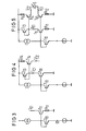
- a source E supplying a variable impressed voltage is assumed at the connection 10 instead of the resonant circuit L, C according to FIG.
- the transistor T 10 connected as a diode is always flowed through by a constant current of, for example, 10 ⁇ A supplied by the current source I.
- a forward voltage of 620 mV is then measured on this transistor T 10 connected as a diode.
- the transistor T 10 connected as a diode and the transistors T 11 , T 12 and T 1 have the same structures.
- the collector currents of the named transistors change in accordance with the known diode equation for the base-emitter path from Transistors. This relationship is plotted by a straight line a in the diagram according to FIG. 6, in which the collector current I c is plotted logarithmically on the ordinate.
- the curve of the collector currents is below the original curve a according to a curve b.
- the voltage drop across the emitter resistors remains significantly less than about 10 mV, the deviation from curve a is hardly noticeable. Due to the logarithmic diode law already mentioned, an increase in the base-emitter control voltage by 1 mV always means an increase in the collector current by 4%. However, the greater the voltage drop across the emitter resistors, the greater the deviation from curve a.
- the voltage drop across the emitter resistor can be greater for the same collector current.
- curves d1 and d2 bend harder from curve c than curve b from curve a for different values of emitter resistance.
- curve a or b correspond to a current mirror according to FIG. 3 or the current mirror T 10 , T 11 , T12 and T 1 (hereinafter also referred to as "current bank").
- the differential current flowing into the output 14 corresponds approximately to the difference between the curves b and d1, d2 according to FIG. 6.
- This fact is shown in FIG. 5 in such a way that the connection of the collectors of the transistors T 14 and T 12 is intended to be separated and the difference between the respective measured by I c2 and I c3 beze i ch- Neten collector current by a measuring instrument S.
- the difference I c2 - I c3 is shown in the diagram according to FIG. 7 for the respective course d1 or d2 according to FIG. 6 in the form of curves gl or g2.
- the currents I c3 and I c2 are represented in the diagram according to FIG.
- the differential current I c2 - I c3 is positive according to the curves gl, g2 in the entire area in the drawing plane to the left of a respective intersection of the curves fl, f2 and e, ie that from the collector of the pnp -Transistor T 14 coming current I c2 is greater than the collector current I c3 of the npn transistor T 12 .
- the Schmitt trigger 20 according to FIG. 2 is activated in this area. Above or to the right of this, the differential current drops sharply and finally changes sign, so that the Schmitt trigger 20 according to FIG. 2 is deactivated.
- the differential current curve gl or g2 practically shows a rectifier characteristic. If the control voltage supplied by the source E according to FIGS. 3 to 5 rises above the point of intersection mentioned above, the npn transistor T 12 saturates. The relationship that the base current is equal to the quotient of the collector current and current gain is then no longer valid. The base current rises considerably, so that the power bank becomes ineffective.
- the feedback path of the oscillator / damping circuit arrangement according to FIG. 2 is via the oscillator Gate amplifier stage forming transistor T 1 and the current mirror T 2 , T 3 , R 3 closed. 3 to 5, the parallel resonance circuit L, C of a proximity switch is located at the input terminal 10 instead of the control signal source E according to FIGS. 3 to 5, as has already been explained at the beginning.
- An increase in the voltage at this resonant circuit causes an increasing current through the transistor T 1 .
- This current is mirrored via the current mirror T 2 , T 31 R 3 and fed back to the resonance circuit (R 3 only has a certain stabilizing effect).
- This current also increases. This in turn leads to an increase in the voltage at the impedance of the resonance circuit, this effect of the tripping being rectified, that is to say it is a positive feedback as is required to trigger each oscillation.
- the circuit arrangement according to FIG. 2 contains several current sources or current sinks in the sense explained, which are controlled together by the control voltage at the input terminal 10.
- the transistors T 13 , T 14 of the second current mirror have different emitter area ratios, the emitter area ratios of the transistor T 13 acting as a reference element and of the controlled transistor T 14 being in particular equal to 1: 4.
- the transistors T 10 , T 11 and T 12 in the first current mirror have the same or not very different emitter area ratios.
- the resistors R 11 , R 12 in the emitter branches of the controlled transistors T 11 , T 12 in the first current mirror are larger than the resistance R 14 in the emitter branch of the controlled transistor T 14 in the second current mirror.
- the current I c2 supplied by this current source is greater than the current I c1 by the factor m if m is the factor by which the emitter area of the transistor T 14 is greater than that of the transistor T l3 . This applies as long as only a negligibly small voltage drop occurs at the corresponding emitter resistor R 14 .
- the current I c2 of this current source rises for large currents due to the then larger voltage drop in a proportionately less than the current I c3 in the transistor T 12 forming a current sink according to FIG. 5. This situation is different in the diagram according to FIG. 7 Values of the resistance R 14 are shown in the respective curve fl or f2, which correspond to the curves dl, d2 according to FIG. 6.
- the subsequent circuit in the form of the Schmitt trigger 20 according to FIG. 2 is controlled by the output connection 14, ie by the connection point of the collectors of the transistors T 14 and T 12 , ie the difference between these two collector currents I c2 and I c3 is used to control the input transistor T 20 of the Schmitt trigger 20 are available.
- the collector current I c2 of the current source T 14 for small currents (that for negative values of the control voltage E) is always greater than the current I c3 of S t roms sink T12.
- the current difference I c2 - I c3 is therefore always positive for negative control voltages E.
- the collector current of the transistor T 14 forming the current source rises only slightly with larger currents, so that the current I c3 outweighs a certain value of the control voltage and - theoretically - there is a negative current difference.
- the voltage rise at the resonance circuit L, C is limited when the above-described saturation of the transistor T 12 acting as a current sink occurs, the impedance then falling on the base rail of the transistors T 11 , T 12 , T 1 , which causes the resonance circuit L, C is drastically (more than a factor of 100) heavier and the gain decreases.
- the amplitude at the resonant circuit has reached its maximum at this limitation, it drops in the same way as it rose before.
- the energy stored in the resonant circuit causes the amplitude in the negative direction to be exactly as large as in the positive direction (a direct current component, ie an asymmetry is not possible on the resonant circuit).
- the level of the limitation is given by the control voltage at which the difference between the impressed currents I c2 - I c3 changes the sign. It is determined by the dimensioning of the emitter resistors R 11 , R 12 , R 14 and the choice of the emitter area ratios in the sense described above.
- the double current mirror according to the invention also acts as a demodulator due to the limiting effect according to curves gl, g2 according to FIG.
- the limitation (see Fig. 7) is temperature stable and is below 200 mV peak-peak. Furthermore, the loop gain is larger and less scattering.
- the impedances at the balancing connection 11 can be chosen to be lower and scatter less than in the circuit arrangement in FIG. 1.
- the demodulation function achieved at the same time is also temperature-stable, since no further diode temperature coefficients have to be taken into account.
- the demodulation curve is steep, which corresponds to a high gain.
- FIG. 8 shows the circuit arrangement according to FIG. 2 with an embodiment of a switching hysteresis implemented according to the invention. To the extent that the same elements in FIG. 8 as in the circuit arrangement according to FIG. 2 are provided with the same reference numerals, reference is made to the explanations for the circuit arrangement according to FIG. 2.
- the Schmitt trigger 20 there is a transistor T 21 with its base on the collector-emitter path of the transistor T 20 , whose emitter is connected to the supply voltage U v (connection 13).
- This transistor T 21 has two , One of which is coupled via a not further b e-recorded resistor to the base of a transistor referred to also not more detail in the Schmitt trigger 20 panels.
- Another collector of the transistor T21 is guided via an amplifier 21 to the inputs of two gates 22 and 23 which act as buffers.
- An antivalent logic output signal is generated at two outputs Q and 0 via these two gates 22 and 23.
- the output of the amplifier 21 is guided to a further gate 24 acting as a buffer, the output of which controls an electronic switch.
- this is a transistor switch T 22 .
- the collector of this switching transistor T 22 is connected to the connection 12 of the circuit via a connection 15 of the circuit arrangement, which leads to the outside, and a variable resistor R H.
- a resistance network can also be provided, which can be switched over to change its total resistance value, for which an electronic switch, such as the transistor T 22 , can be used.
- the oscillator and demodulator are functionally coupled to one another in a non-separable manner, so that the relationships distance / oscillation amplitude, oscillation amplitude / demodulator current, demodulator current / switching point are so clearly fixed on circuit and geometry relationships are that by switching the demodulator circuit an unambiguous assignment of the hysteresis to the distance, that is, a distance hysteresis without observable influence of tolerances or fluctuations in the absolute values of the components or the current amplification of transistors is realized.
- the adjustable resistance R H which depending on the output signal of the Schmitt trigger 20 when the switching transistor T 22 is conductive or blocked, is either coupled from the circuit output 14 to ground or ineffective .
- the hysteresis and the distance can thus be set independently of one another via the resistors R A and R H.
- the resistance R H responsible for the hysteresis is not in the emitter circuit of the transistor amplifier stage T 1 , so that no oscillation amplitudes occur on it and the parasitic capacitances associated therewith do not affect the oscillation behavior of the oscillator can influence more.
Landscapes
- Electronic Switches (AREA)
- Arrangements For Transmission Of Measured Signals (AREA)
- Geophysics And Detection Of Objects (AREA)
- Stabilization Of Oscillater, Synchronisation, Frequency Synthesizers (AREA)
- Inductance-Capacitance Distribution Constants And Capacitance-Resistance Oscillators (AREA)
Priority Applications (1)
| Application Number | Priority Date | Filing Date | Title |
|---|---|---|---|
| AT86108311T ATE56328T1 (de) | 1985-06-20 | 1986-06-18 | Oszillator/demodulator-schaltungsanordnung fuer einen induktiven annaeherungsschalter. |
Applications Claiming Priority (2)
| Application Number | Priority Date | Filing Date | Title |
|---|---|---|---|
| DE3522120 | 1985-06-20 | ||
| DE3522120 | 1985-06-20 |
Publications (2)
| Publication Number | Publication Date |
|---|---|
| EP0207372A1 true EP0207372A1 (fr) | 1987-01-07 |
| EP0207372B1 EP0207372B1 (fr) | 1990-09-05 |
Family
ID=6273759
Family Applications (1)
| Application Number | Title | Priority Date | Filing Date |
|---|---|---|---|
| EP86108311A Expired - Lifetime EP0207372B1 (fr) | 1985-06-20 | 1986-06-18 | Montage oscillateur/démodulateur pour un commutateur de proximité de type inductif |
Country Status (6)
| Country | Link |
|---|---|
| US (1) | US4806882A (fr) |
| EP (1) | EP0207372B1 (fr) |
| JP (1) | JPS61295719A (fr) |
| AT (1) | ATE56328T1 (fr) |
| DE (1) | DE3673892D1 (fr) |
| DK (1) | DK288486A (fr) |
Cited By (2)
| Publication number | Priority date | Publication date | Assignee | Title |
|---|---|---|---|---|
| EP0404065A1 (fr) * | 1989-06-21 | 1990-12-27 | Omron Corporation | Capteur à circuit oscillant |
| EP0463188A1 (fr) * | 1990-06-19 | 1992-01-02 | Siemens Aktiengesellschaft | Commutateur de proximité inductif peu sensible aux variations de température |
Families Citing this family (6)
| Publication number | Priority date | Publication date | Assignee | Title |
|---|---|---|---|---|
| US5341129A (en) * | 1991-11-07 | 1994-08-23 | Rpm Detection, Inc. | Zero-motion detection proximity switch |
| GB2263549B (en) * | 1991-12-31 | 1996-04-03 | Square D Co | Improvements in and relating to proximity switches |
| US5418495A (en) * | 1994-05-18 | 1995-05-23 | Elantec | Input stage improvement for current feedback amplifiers |
| US5578967A (en) * | 1995-09-28 | 1996-11-26 | Elantec | Circuit compensating for capacitance at inverting input of current feedback amplifier |
| JP2003526701A (ja) * | 1998-11-18 | 2003-09-09 | コーニンクレッカ フィリップス エレクトロニクス エヌ ヴィ | 蛍光材料 |
| US20030058604A1 (en) * | 2001-09-13 | 2003-03-27 | Canagasaby Karthisha S. | Method and apparatus to emulate external IO interconnection |
Citations (2)
| Publication number | Priority date | Publication date | Assignee | Title |
|---|---|---|---|---|
| GB2075201A (en) * | 1980-05-02 | 1981-11-11 | Honeywell Gmbh | Electronic proximity switch |
| EP0172393A1 (fr) * | 1984-07-13 | 1986-02-26 | Siemens Aktiengesellschaft | Circuit oscillateur-démodulateur pour un commutateur de proximité inductif |
Family Cites Families (3)
| Publication number | Priority date | Publication date | Assignee | Title |
|---|---|---|---|---|
| CH421237A (de) * | 1964-02-05 | 1966-09-30 | Ebauches Sa | Näherungsdetektor |
| US4543527A (en) * | 1982-04-12 | 1985-09-24 | Eaton Corporation | Proximity switch exhibiting improved start-up characteristics |
| DE3327329C2 (de) * | 1983-07-29 | 1987-02-12 | Robert 7995 Neukirch Buck | Elektronisches, vorzugsweise berührungslos arbeitendes Schaltgerät |
-
1986
- 1986-06-13 JP JP61138009A patent/JPS61295719A/ja active Granted
- 1986-06-18 AT AT86108311T patent/ATE56328T1/de not_active IP Right Cessation
- 1986-06-18 DE DE8686108311T patent/DE3673892D1/de not_active Expired - Lifetime
- 1986-06-18 EP EP86108311A patent/EP0207372B1/fr not_active Expired - Lifetime
- 1986-06-19 US US06/876,376 patent/US4806882A/en not_active Expired - Fee Related
- 1986-06-19 DK DK288486A patent/DK288486A/da not_active Application Discontinuation
Patent Citations (2)
| Publication number | Priority date | Publication date | Assignee | Title |
|---|---|---|---|---|
| GB2075201A (en) * | 1980-05-02 | 1981-11-11 | Honeywell Gmbh | Electronic proximity switch |
| EP0172393A1 (fr) * | 1984-07-13 | 1986-02-26 | Siemens Aktiengesellschaft | Circuit oscillateur-démodulateur pour un commutateur de proximité inductif |
Non-Patent Citations (2)
| Title |
|---|
| ELECTRONIQUE & APPLICATIONS INDUSTRIELLES, Nr. 233, 15. März 1977, Seite 63, Paris, FR: "Les détecteurs de proximité et de passage à fente" * |
| ELECTRONIQUE ET MICROELECTRONIQUE INDUSTRIELLES, Nr. 207, 15. Juni 1975, Seiten 54-56, Paris, FR; J.M. ZULAUF: "Réalisez votre détecteur de proximité à seuils réglables" * |
Cited By (2)
| Publication number | Priority date | Publication date | Assignee | Title |
|---|---|---|---|---|
| EP0404065A1 (fr) * | 1989-06-21 | 1990-12-27 | Omron Corporation | Capteur à circuit oscillant |
| EP0463188A1 (fr) * | 1990-06-19 | 1992-01-02 | Siemens Aktiengesellschaft | Commutateur de proximité inductif peu sensible aux variations de température |
Also Published As
| Publication number | Publication date |
|---|---|
| ATE56328T1 (de) | 1990-09-15 |
| DE3673892D1 (de) | 1990-10-11 |
| DK288486A (da) | 1986-12-21 |
| EP0207372B1 (fr) | 1990-09-05 |
| US4806882A (en) | 1989-02-21 |
| JPH0551211B2 (fr) | 1993-08-02 |
| DK288486D0 (da) | 1986-06-19 |
| JPS61295719A (ja) | 1986-12-26 |
Similar Documents
| Publication | Publication Date | Title |
|---|---|---|
| EP0096944B1 (fr) | Circuit avec plusieurs chemins de signaux formés par des composants actifs | |
| DE2323478A1 (de) | Datenuebertragungsanordnung | |
| EP0529118B1 (fr) | Circuit de régulation de courant | |
| DE69311824T2 (de) | Schaltung mit veränderlicher Verzögerung | |
| EP0172393B1 (fr) | Circuit oscillateur-démodulateur pour un commutateur de proximité inductif | |
| DE3016821C2 (de) | Elektronischer Näherungsschalter | |
| EP0591750A2 (fr) | Méthode pour régler le courant d'un circuit d'attaque de sortie intégré monolithique | |
| DE2352587A1 (de) | Verstaerker mit steuerbarer verstaerkung | |
| DE2305291C3 (de) | Regelschaltung zur Regelung der Amplitude eines Signals | |
| EP0207372B1 (fr) | Montage oscillateur/démodulateur pour un commutateur de proximité de type inductif | |
| DE3842288A1 (de) | Schaltungsanordnung zur erzeugung einer konstanten bezugsspannung | |
| DE2402721C3 (de) | Kapazitiver Näherungsdetektor | |
| DE68923334T2 (de) | Stromschalterlogikschaltung mit gesteuerten Ausgangssignalpegeln. | |
| DE2548457A1 (de) | Konstantspannungsschaltung | |
| DE3904910C2 (fr) | ||
| WO1998025346A1 (fr) | Commutateur electronique sans contact | |
| EP0025029B1 (fr) | Dispositif de pont de mesure capacitif | |
| DE1921936A1 (de) | Elektrischer Schaltkreis,insbesondere Differentialverstaerkerstufe | |
| DE2301855B2 (de) | Schaltungsanordnung mit Feldeffekttransistoren zur Pegelanpassung | |
| DE2820416C2 (de) | Tristabiler Schaltkreis | |
| DE3844387C2 (de) | Schaltung zur Erzeugung einer über weite Bereiche der Versorgungsspannung konstanten Bezugsspannung, insb. für einen dynamischen Direktzugriffsspeicher | |
| DE2721836A1 (de) | Temperaturkompensierter kristalloszillator | |
| DE4039422C2 (de) | Magnetfeldsensor | |
| DE2361809B2 (de) | Verstärkungsreglerschaltung | |
| DE1513670B2 (de) | Schaltungsanordnung zur Regelung eines durch einen Verbraucher fließenden elektrischen Stromes |
Legal Events
| Date | Code | Title | Description |
|---|---|---|---|
| PUAI | Public reference made under article 153(3) epc to a published international application that has entered the european phase |
Free format text: ORIGINAL CODE: 0009012 |
|
| AK | Designated contracting states |
Kind code of ref document: A1 Designated state(s): AT CH DE FR GB IT LI NL SE |
|
| 17P | Request for examination filed |
Effective date: 19870127 |
|
| 17Q | First examination report despatched |
Effective date: 19881216 |
|
| GRAA | (expected) grant |
Free format text: ORIGINAL CODE: 0009210 |
|
| AK | Designated contracting states |
Kind code of ref document: B1 Designated state(s): AT CH DE FR GB IT LI NL SE |
|
| REF | Corresponds to: |
Ref document number: 56328 Country of ref document: AT Date of ref document: 19900915 Kind code of ref document: T |
|
| REF | Corresponds to: |
Ref document number: 3673892 Country of ref document: DE Date of ref document: 19901011 |
|
| ET | Fr: translation filed | ||
| ITF | It: translation for a ep patent filed | ||
| GBT | Gb: translation of ep patent filed (gb section 77(6)(a)/1977) | ||
| ITTA | It: last paid annual fee | ||
| PLBE | No opposition filed within time limit |
Free format text: ORIGINAL CODE: 0009261 |
|
| STAA | Information on the status of an ep patent application or granted ep patent |
Free format text: STATUS: NO OPPOSITION FILED WITHIN TIME LIMIT |
|
| 26N | No opposition filed | ||
| PGFP | Annual fee paid to national office [announced via postgrant information from national office to epo] |
Ref country code: GB Payment date: 19920521 Year of fee payment: 7 |
|
| PGFP | Annual fee paid to national office [announced via postgrant information from national office to epo] |
Ref country code: AT Payment date: 19920529 Year of fee payment: 7 |
|
| PGFP | Annual fee paid to national office [announced via postgrant information from national office to epo] |
Ref country code: SE Payment date: 19920616 Year of fee payment: 7 |
|
| PGFP | Annual fee paid to national office [announced via postgrant information from national office to epo] |
Ref country code: FR Payment date: 19920624 Year of fee payment: 7 |
|
| PGFP | Annual fee paid to national office [announced via postgrant information from national office to epo] |
Ref country code: NL Payment date: 19920630 Year of fee payment: 7 |
|
| PGFP | Annual fee paid to national office [announced via postgrant information from national office to epo] |
Ref country code: DE Payment date: 19920824 Year of fee payment: 7 |
|
| PGFP | Annual fee paid to national office [announced via postgrant information from national office to epo] |
Ref country code: CH Payment date: 19920914 Year of fee payment: 7 |
|
| PG25 | Lapsed in a contracting state [announced via postgrant information from national office to epo] |
Ref country code: GB Effective date: 19930618 Ref country code: AT Effective date: 19930618 |
|
| PG25 | Lapsed in a contracting state [announced via postgrant information from national office to epo] |
Ref country code: SE Effective date: 19930619 |
|
| PG25 | Lapsed in a contracting state [announced via postgrant information from national office to epo] |
Ref country code: LI Effective date: 19930630 Ref country code: CH Effective date: 19930630 |
|
| PG25 | Lapsed in a contracting state [announced via postgrant information from national office to epo] |
Ref country code: NL Effective date: 19940101 |
|
| GBPC | Gb: european patent ceased through non-payment of renewal fee |
Effective date: 19930618 |
|
| NLV4 | Nl: lapsed or anulled due to non-payment of the annual fee | ||
| PG25 | Lapsed in a contracting state [announced via postgrant information from national office to epo] |
Ref country code: FR Effective date: 19940228 |
|
| REG | Reference to a national code |
Ref country code: CH Ref legal event code: PL |
|
| PG25 | Lapsed in a contracting state [announced via postgrant information from national office to epo] |
Ref country code: DE Effective date: 19940301 |
|
| REG | Reference to a national code |
Ref country code: FR Ref legal event code: ST |
|
| EUG | Se: european patent has lapsed |
Ref document number: 86108311.1 Effective date: 19940110 |
|
| PG25 | Lapsed in a contracting state [announced via postgrant information from national office to epo] |
Ref country code: IT Free format text: LAPSE BECAUSE OF NON-PAYMENT OF DUE FEES Effective date: 20050618 |