EP0207699A2 - Dispositif émetteur de lumière comportant une structure à puits quantiques multiples - Google Patents
Dispositif émetteur de lumière comportant une structure à puits quantiques multiples Download PDFInfo
- Publication number
- EP0207699A2 EP0207699A2 EP86304772A EP86304772A EP0207699A2 EP 0207699 A2 EP0207699 A2 EP 0207699A2 EP 86304772 A EP86304772 A EP 86304772A EP 86304772 A EP86304772 A EP 86304772A EP 0207699 A2 EP0207699 A2 EP 0207699A2
- Authority
- EP
- European Patent Office
- Prior art keywords
- light
- quantum well
- emitting element
- multiquantum
- well
- Prior art date
- Legal status (The legal status is an assumption and is not a legal conclusion. Google has not performed a legal analysis and makes no representation as to the accuracy of the status listed.)
- Withdrawn
Links
Images
Classifications
-
- H—ELECTRICITY
- H10—SEMICONDUCTOR DEVICES; ELECTRIC SOLID-STATE DEVICES NOT OTHERWISE PROVIDED FOR
- H10H—INORGANIC LIGHT-EMITTING SEMICONDUCTOR DEVICES HAVING POTENTIAL BARRIERS
- H10H20/00—Individual inorganic light-emitting semiconductor devices having potential barriers, e.g. light-emitting diodes [LED]
- H10H20/80—Constructional details
- H10H20/81—Bodies
- H10H20/811—Bodies having quantum effect structures or superlattices, e.g. tunnel junctions
- H10H20/812—Bodies having quantum effect structures or superlattices, e.g. tunnel junctions within the light-emitting regions, e.g. having quantum confinement structures
-
- B—PERFORMING OPERATIONS; TRANSPORTING
- B82—NANOTECHNOLOGY
- B82Y—SPECIFIC USES OR APPLICATIONS OF NANOSTRUCTURES; MEASUREMENT OR ANALYSIS OF NANOSTRUCTURES; MANUFACTURE OR TREATMENT OF NANOSTRUCTURES
- B82Y20/00—Nanooptics, e.g. quantum optics or photonic crystals
-
- H—ELECTRICITY
- H01—ELECTRIC ELEMENTS
- H01S—DEVICES USING THE PROCESS OF LIGHT AMPLIFICATION BY STIMULATED EMISSION OF RADIATION [LASER] TO AMPLIFY OR GENERATE LIGHT; DEVICES USING STIMULATED EMISSION OF ELECTROMAGNETIC RADIATION IN WAVE RANGES OTHER THAN OPTICAL
- H01S5/00—Semiconductor lasers
- H01S5/10—Construction or shape of the optical resonator, e.g. extended or external cavity, coupled cavities, bent-guide, varying width, thickness or composition of the active region
- H01S5/18—Surface-emitting [SE] lasers, e.g. having both horizontal and vertical cavities
- H01S5/183—Surface-emitting [SE] lasers, e.g. having both horizontal and vertical cavities having only vertical cavities, e.g. vertical cavity surface-emitting lasers [VCSEL]
-
- H—ELECTRICITY
- H10—SEMICONDUCTOR DEVICES; ELECTRIC SOLID-STATE DEVICES NOT OTHERWISE PROVIDED FOR
- H10H—INORGANIC LIGHT-EMITTING SEMICONDUCTOR DEVICES HAVING POTENTIAL BARRIERS
- H10H20/00—Individual inorganic light-emitting semiconductor devices having potential barriers, e.g. light-emitting diodes [LED]
-
- H—ELECTRICITY
- H01—ELECTRIC ELEMENTS
- H01S—DEVICES USING THE PROCESS OF LIGHT AMPLIFICATION BY STIMULATED EMISSION OF RADIATION [LASER] TO AMPLIFY OR GENERATE LIGHT; DEVICES USING STIMULATED EMISSION OF ELECTROMAGNETIC RADIATION IN WAVE RANGES OTHER THAN OPTICAL
- H01S5/00—Semiconductor lasers
- H01S5/30—Structure or shape of the active region; Materials used for the active region
- H01S5/34—Structure or shape of the active region; Materials used for the active region comprising quantum well or superlattice structures, e.g. single quantum well [SQW] lasers, multiple quantum well [MQW] lasers or graded index separate confinement heterostructure [GRINSCH] lasers
- H01S5/3415—Structure or shape of the active region; Materials used for the active region comprising quantum well or superlattice structures, e.g. single quantum well [SQW] lasers, multiple quantum well [MQW] lasers or graded index separate confinement heterostructure [GRINSCH] lasers containing details related to carrier capture times into wells or barriers
-
- H—ELECTRICITY
- H01—ELECTRIC ELEMENTS
- H01S—DEVICES USING THE PROCESS OF LIGHT AMPLIFICATION BY STIMULATED EMISSION OF RADIATION [LASER] TO AMPLIFY OR GENERATE LIGHT; DEVICES USING STIMULATED EMISSION OF ELECTROMAGNETIC RADIATION IN WAVE RANGES OTHER THAN OPTICAL
- H01S5/00—Semiconductor lasers
- H01S5/30—Structure or shape of the active region; Materials used for the active region
- H01S5/34—Structure or shape of the active region; Materials used for the active region comprising quantum well or superlattice structures, e.g. single quantum well [SQW] lasers, multiple quantum well [MQW] lasers or graded index separate confinement heterostructure [GRINSCH] lasers
- H01S5/343—Structure or shape of the active region; Materials used for the active region comprising quantum well or superlattice structures, e.g. single quantum well [SQW] lasers, multiple quantum well [MQW] lasers or graded index separate confinement heterostructure [GRINSCH] lasers in AIIIBV compounds, e.g. AlGaAs-laser, InP-based laser
- H01S5/34313—Structure or shape of the active region; Materials used for the active region comprising quantum well or superlattice structures, e.g. single quantum well [SQW] lasers, multiple quantum well [MQW] lasers or graded index separate confinement heterostructure [GRINSCH] lasers in AIIIBV compounds, e.g. AlGaAs-laser, InP-based laser with a well layer having only As as V-compound, e.g. AlGaAs, InGaAs
- H01S5/3432—Structure or shape of the active region; Materials used for the active region comprising quantum well or superlattice structures, e.g. single quantum well [SQW] lasers, multiple quantum well [MQW] lasers or graded index separate confinement heterostructure [GRINSCH] lasers in AIIIBV compounds, e.g. AlGaAs-laser, InP-based laser with a well layer having only As as V-compound, e.g. AlGaAs, InGaAs the whole junction comprising only (AI)GaAs
Definitions
- the present invention relates to a light-emitting element, and particularly to a light-emitting element such as a light-emitting diode or a semiconductor laser having a multiquantum-well structure in the light-emitting region.
- LED's Conventional semiconductor lasers and light-emitting diodes (hereinafter referred to as LED's) have been realized with a structure consisting of a pn junction of the same material or with a single-heterostructure or a double-heterostructure in which one side of the pn junction or both sides of the light-emitting region (active region) are constituted by a material having a high energy bandgap.
- Objects that may be achievable by preferred embodiments of the invention include the following: to provide a light-emitting element, particularly a semiconductor laser, a light-emitting diode, or the like, having a high light generation efficiency; to provide a semiconductor laser or a light-emitting diode having a high light generation efficiency and a low threshold current, and to realize a light source that can be adapted to lightwave communications, optical discs and facsimiles.
- the present invention deals with a semiconductor light emitting device, e.g. a laser or a light-emitting diode, having a multiquantum-well structure constituted by compound semiconductor layers, wherein the quantum well width which constitutes the quantum well or the energy difference (barrier height) between a barrier layer and a quantum well layer, is so selected that the highest level among the quantum levels in the quantum well is not brought into agreement with the energy level (uppermost end of the valence band or lowermost end of the conduction band) of the barrier layer.
- a semiconductor light emitting device e.g. a laser or a light-emitting diode
- the quantum well width which constitutes the quantum well or the energy difference (barrier height) between a barrier layer and a quantum well layer, is so selected that the highest level among the quantum levels in the quantum well is not brought into agreement with the energy level (uppermost end of the valence band or lowermost end of the conduction band) of the
- the above effect stems from the fact that the energy levels of electrons and holes formed in the quantum well change with the change in the quantum well width, and are deviated from the barrier height, causing the carrier injection into the quantum well to be promoted. Therefore, if a quantum well laser is fabricated by selecting the quantum well width that exhibits the above low threshold current, there can be realized a semiconductor laser device that exhibits a high quantum efficiency with a small threshold current, that could not be implied thus far.
- the present invention deals with a semiconductor laser device having multiquantum-well structure which employs a compound semiconductor, wherein the quantum well width which constitutes the quantum well or the energy difference (barrier height) between a barrier layer and a quantum well layer, is so selected that the highest level among the quantum levels in the quantum well is not brought into agreement with the energy level of the barrier layer, so that the carrier injection into the quantum well is promoted, the threshold current is greatly reduced, and that the differential quantum efficiency increases.
- the present invention further provides an LED which employs the multiquantum well structure in the light-emitting region, the LED having a quantum well width of an optimum light generation efficiency.
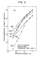
- Fig. 3 shows the dependency of photoluminescence (PL) intensity I PL upon the excitation intensity I EX when the width of the Al 0.3 Ga 0.7 As barrier layer (or confinement layer) is maintained constant and when the width of the GaAs quantum well layer (or active layer) is changed in a GaAs/Al 0.3 Ga 0.7 As multiquantum well.
- Fig. 4 shows the dependency of PL upon the exciting light intensity (I PL ⁇ I EX m ), i.e., shows the dependency of index (proportional constant of the logarithmic notation) upon the quantum well width.
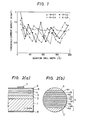
- Fig. 2 is a section view which illustrates a semiconductor laser device according to an embodiment of the present invention, wherein Fig. 2(a) is a diagram showing the whole device, and Fig. 2(b) is a diagram showing an encircled portion thereof on an enlarged scale. As shown in Figs.
- n+-GaAs buffer layer 0.5 ⁇ m
- n-type impurity concentration of 2 x 1018 cm ⁇ 3 2(a) and 2(b), on a (100)n+-GaAs substrate (doped with silicon at a concentration of about 2 x 1018 cm ⁇ 3) 1 are grown as n+-GaAs buffer layer (0.5 ⁇ m) thick, n-type impurity concentration of 2 x 1018 cm ⁇ 3) 2, an n-Al 0.5 Ga 0.5 As cladding layer (0.5 ⁇ m thick, n-type impurity concentration of 1 x 1018 cm ⁇ 3) 3, an undoped multiquantum-well layer [consisting of five Al 0.3 Ga 0.7 As layers (each 100 angstroms thick) 4a and four GaAs layers (each 74 angstroms thick) 4b that are alternatingly lamintated] 4, a p-Al 0.5 Ga 0.5 As cladding layer (1 ⁇ m thick,
- the GaAs is grown at a rate of 1 ⁇ m per hour.
- a striped AuAgZn electrode 7 having a size of 5 ⁇ m x 300 ⁇ m and an AuGeNi electrode 8 on the back surface thereof by vacuum evaporation.
- a semiconductor laser device of the gain induced stripe type having a quantum well width of 74 angstroms as described above.
- the thus fabricated semiconductor laser device exhibits a threshold current density of as small as 650 A/cm2.
- the threshold current density increases to larger than 900 A/cm2.
- the semiconductor laser device having the quantum well width of 72 angstroms of this embodiment exhibits a differential quantum efficiency which is increased by about 10% compared with other semiconductor laser devices having quantum well widths of 50 angstroms and 90 angstroms.
- the threshold current can be decreased and the differential quantum efficiency can be increased. If an optimum quantum well width is selected as described above, substantially the same effects can be exhibited even with the laser device of any other stripe structure such as graded index type laser, buried heterostructure laser, and the like lasers.
- the above embodiment has employed materials of the AlGaAs/GaAs type, the same effects can also be obtained by selecting such a quantum well width that increases the carrier injection into the quantum well layer even when materials of other compound semiconductor types are used such as Al x Ga 1-x As/Al y Ga 1-y As; In x Ga 1-x AsP 1-y /InP, In x Ga 1-x As/In y Al 1-y As; and In x Ga 1-x P/In y Al 1-y P.
- materials of other compound semiconductor types such as Al x Ga 1-x As/Al y Ga 1-y As; In x Ga 1-x AsP 1-y /InP, In x Ga 1-x As/In y Al 1-y As; and In x Ga 1-x P/In y Al 1-y P.
- the quantum well width which constitutes the quantum well or the energy difference between a barrier layer and a quantum well layer is so selected that the highest level among the quantum levels in the quantum well is not brought into agreement with the energy level of the barrier, so that the energy level of electrons and holes formed in the quantum well helps promote the carrier injection into the quantum well regardless of the barrier height. Therefore, there can be fabricated a quantum well type semiconductor laser which permits a greatly reduced threshold current to flow and which exhibits a quantum efficiency that is increased by about 10%.
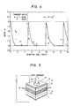
- Fig. 5 illustrates the structure of an LED according to the present invention, wherein reference numeral 11 denotes an ohmic contact electrode of the n-type side, 12 denotes an n+-type GaAs substrate, and 13 denotes an n+-type Al 0.3 Ga 0.7 As layer.
- a light-emitting region of multiquantum well is constituted by undoped GaAs layers 14 and undoped Al 0.3 Ga 0.7 As layers 15.
- Each GaAs layer has a thickness of 75 angstroms and each Al 0.3 Ga 0.7 As barrier layer has a thickness of 300 angstroms so that a value of m will be about 1 as shown in Fig. 4.
- the LED of this embodiement uses four GaAs layers and five Al 0.3 Ga 0.7 As layers.
- Reference numeral 16 denotes a p+-type Al 0.3 Ga 0.7 As layer
- 17 denotes a p+-type GaAs layer for ohmic contact
- 18 denotes an ohmic-contact electrode of the p-type side.
- the LED structure according to this embodiment is fabricated by the molecular beam epitaxy (MBE).
- MBE molecular beam epitaxy
- the positive side of the power source is connected to the contact electrode of the p-type side
- the negative side of the power source is connected to the contact electrode of the n-type side, so that light 20 is emitted from the multiquantum-well region through a light-emitting window 19.
- the p+-type GaAs layer for ohmic contact under the window 19 has been removed by etching, so that the light that is emitted is not interrupted.
- the LED produces an optical output of 1.5 mW when the drive current is 50 mA.
- the output of 1.5 mW is about 1.5 times as great as that of the LED of the same structure but which does not have an optimum well width.
- a multiquantum-well type LED can be fabricated having a quantum well width which produces the greatest light generation efficiency, the LED being driven on a small current.
Landscapes
- Physics & Mathematics (AREA)
- Nanotechnology (AREA)
- Engineering & Computer Science (AREA)
- Chemical & Material Sciences (AREA)
- Optics & Photonics (AREA)
- Biophysics (AREA)
- Life Sciences & Earth Sciences (AREA)
- Electromagnetism (AREA)
- General Physics & Mathematics (AREA)
- Crystallography & Structural Chemistry (AREA)
- Condensed Matter Physics & Semiconductors (AREA)
- Semiconductor Lasers (AREA)
- Led Devices (AREA)
Applications Claiming Priority (4)
| Application Number | Priority Date | Filing Date | Title |
|---|---|---|---|
| JP14038485A JPS622581A (ja) | 1985-06-28 | 1985-06-28 | 半導体レ−ザ装置 |
| JP140384/85 | 1985-06-28 | ||
| JP8790886A JPH07120818B2 (ja) | 1986-04-18 | 1986-04-18 | 発光ダイオ−ド |
| JP87908/86 | 1986-04-18 |
Publications (2)
| Publication Number | Publication Date |
|---|---|
| EP0207699A2 true EP0207699A2 (fr) | 1987-01-07 |
| EP0207699A3 EP0207699A3 (fr) | 1989-03-08 |
Family
ID=26429135
Family Applications (1)
| Application Number | Title | Priority Date | Filing Date |
|---|---|---|---|
| EP86304772A Withdrawn EP0207699A3 (fr) | 1985-06-28 | 1986-06-20 | Dispositif émetteur de lumière comportant une structure à puits quantiques multiples |
Country Status (1)
| Country | Link |
|---|---|
| EP (1) | EP0207699A3 (fr) |
Cited By (3)
| Publication number | Priority date | Publication date | Assignee | Title |
|---|---|---|---|---|
| EP0412120A4 (en) * | 1988-04-22 | 1991-03-20 | University Of New Mexico | Wavelength-resonant surface-emitting semiconductor laser |
| WO1992016024A3 (fr) * | 1991-03-11 | 1992-11-12 | Boeing Co | Del de puits quantiques a large bande |
| EP0611494A4 (en) * | 1991-11-07 | 1994-09-21 | Bandgap Tech Corp | Visible light surface emitting semiconductor laser. |
Family Cites Families (1)
| Publication number | Priority date | Publication date | Assignee | Title |
|---|---|---|---|---|
| US4163238A (en) * | 1978-06-09 | 1979-07-31 | The United States Of America As Represented By The Secretary Of The Army | Infrared semiconductor device with superlattice region |
-
1986
- 1986-06-20 EP EP86304772A patent/EP0207699A3/fr not_active Withdrawn
Cited By (3)
| Publication number | Priority date | Publication date | Assignee | Title |
|---|---|---|---|---|
| EP0412120A4 (en) * | 1988-04-22 | 1991-03-20 | University Of New Mexico | Wavelength-resonant surface-emitting semiconductor laser |
| WO1992016024A3 (fr) * | 1991-03-11 | 1992-11-12 | Boeing Co | Del de puits quantiques a large bande |
| EP0611494A4 (en) * | 1991-11-07 | 1994-09-21 | Bandgap Tech Corp | Visible light surface emitting semiconductor laser. |
Also Published As
| Publication number | Publication date |
|---|---|
| EP0207699A3 (fr) | 1989-03-08 |
Similar Documents
| Publication | Publication Date | Title |
|---|---|---|
| US5936266A (en) | Semiconductor devices and methods with tunnel contact hole sources | |
| US5892787A (en) | N-drive, p-common light-emitting devices fabricated on an n-type substrate and method of making same | |
| KR101020387B1 (ko) | 반도체 메사 구조와 도전형 접합을 포함하는 전자 소자 및그 제조방법 | |
| US5488233A (en) | Semiconductor light-emitting device with compound semiconductor layer | |
| US5010374A (en) | Quantum well laser utilizing an inversion layer | |
| US6369403B1 (en) | Semiconductor devices and methods with tunnel contact hole sources and non-continuous barrier layer | |
| Allerman et al. | InAsSb‐based mid‐infrared lasers (3.8–3.9 μm) and light‐emitting diodes with AlAsSb claddings and semimetal electron injection, grown by metalorganic chemical vapor deposition | |
| US6853663B2 (en) | Efficiency GaN-based light emitting devices | |
| USRE38339E1 (en) | Semiconductor laser | |
| EP1204150B1 (fr) | Procédé de fabrication d'une LED à semi-conducteur avec une hétérostructure encollée | |
| US5617446A (en) | Surface-emitting semiconductor light emitting device | |
| EP0605051B1 (fr) | Laser à injection émettant dans le bleu-vert | |
| CN1259237A (zh) | 光电子半导体元件 | |
| JP2000277855A (ja) | 半導体発光素子 | |
| US4602370A (en) | Large optical cavity laser having a plurality of active layers | |
| EP0610893B1 (fr) | Diode à laser | |
| US6931044B2 (en) | Method and apparatus for improving temperature performance for GaAsSb/GaAs devices | |
| US5138624A (en) | Multiwavelength LED and laser diode optical source | |
| JP3486193B2 (ja) | 光電半導体素子 | |
| US4313125A (en) | Light emitting semiconductor devices | |
| US7103080B2 (en) | Laser diode with a low absorption diode junction | |
| US5250814A (en) | Semiconductor light-emitting devices | |
| US20230006426A1 (en) | Group iii-n light emitter electrically injected by hot carriers from auger recombination | |
| EP0207699A2 (fr) | Dispositif émetteur de lumière comportant une structure à puits quantiques multiples | |
| US7986721B2 (en) | Semiconductor optical device including a PN junction formed by a second region of a first conductive type semiconductor layer and a second conductive type single semiconductor layer |
Legal Events
| Date | Code | Title | Description |
|---|---|---|---|
| PUAI | Public reference made under article 153(3) epc to a published international application that has entered the european phase |
Free format text: ORIGINAL CODE: 0009012 |
|
| 17P | Request for examination filed |
Effective date: 19860711 |
|
| AK | Designated contracting states |
Kind code of ref document: A2 Designated state(s): DE FR GB |
|
| PUAL | Search report despatched |
Free format text: ORIGINAL CODE: 0009013 |
|
| AK | Designated contracting states |
Kind code of ref document: A3 Designated state(s): DE FR GB |
|
| STAA | Information on the status of an ep patent application or granted ep patent |
Free format text: STATUS: THE APPLICATION IS DEEMED TO BE WITHDRAWN |
|
| 18D | Application deemed to be withdrawn |
Effective date: 19890909 |
|
| RIN1 | Information on inventor provided before grant (corrected) |
Inventor name: KATAYAMA, YOSHIFUMI Inventor name: SHIRAKI, YASUHIRO Inventor name: SAWADA, YASUSHI Inventor name: MURAYAMA, YOSHIMASA Inventor name: MORIOKA, MAKOTO Inventor name: KASAI, JUNICHI Inventor name: MISHIMA, TOMOYOSHI |