EP0210373B1 - Kalibrierter Stromdetektor - Google Patents
Kalibrierter Stromdetektor Download PDFInfo
- Publication number
- EP0210373B1 EP0210373B1 EP86107282A EP86107282A EP0210373B1 EP 0210373 B1 EP0210373 B1 EP 0210373B1 EP 86107282 A EP86107282 A EP 86107282A EP 86107282 A EP86107282 A EP 86107282A EP 0210373 B1 EP0210373 B1 EP 0210373B1
- Authority
- EP
- European Patent Office
- Prior art keywords
- detector
- signal
- alternating signal
- voltage
- set forth
- Prior art date
- Legal status (The legal status is an assumption and is not a legal conclusion. Google has not performed a legal analysis and makes no representation as to the accuracy of the status listed.)
- Expired
Links
- 230000001419 dependent effect Effects 0.000 claims description 4
- 230000001105 regulatory effect Effects 0.000 claims description 4
- 230000007274 generation of a signal involved in cell-cell signaling Effects 0.000 claims 6
- 238000001514 detection method Methods 0.000 claims 1
- 230000000063 preceeding effect Effects 0.000 claims 1
- 238000010586 diagram Methods 0.000 description 9
- 239000003990 capacitor Substances 0.000 description 8
- 230000005669 field effect Effects 0.000 description 7
- 230000008901 benefit Effects 0.000 description 4
- 238000000034 method Methods 0.000 description 4
- 230000004044 response Effects 0.000 description 3
- 230000005540 biological transmission Effects 0.000 description 2
- 230000001276 controlling effect Effects 0.000 description 2
- 230000004913 activation Effects 0.000 description 1
- 230000008859 change Effects 0.000 description 1
- 238000010276 construction Methods 0.000 description 1
- 238000005259 measurement Methods 0.000 description 1
- 230000010355 oscillation Effects 0.000 description 1
- 238000007493 shaping process Methods 0.000 description 1
- 238000004148 unit process Methods 0.000 description 1
Images

Classifications
-
- G—PHYSICS
- G01—MEASURING; TESTING
- G01R—MEASURING ELECTRIC VARIABLES; MEASURING MAGNETIC VARIABLES
- G01R21/00—Arrangements for measuring electric power or power factor
- G01R21/10—Arrangements for measuring electric power or power factor by using square-law characteristics of circuit elements, e.g. diodes, to measure power absorbed by loads of known impedance
-
- G—PHYSICS
- G01—MEASURING; TESTING
- G01R—MEASURING ELECTRIC VARIABLES; MEASURING MAGNETIC VARIABLES
- G01R35/00—Testing or calibrating of apparatus covered by the other groups of this subclass
- G01R35/04—Testing or calibrating of apparatus covered by the other groups of this subclass of instruments for measuring time integral of power or current
Definitions
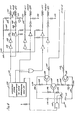
- the operational amplifier 34 also has a pair of input terminals one of which is connected to a first terminal of an impedance 38, the second terminal of the impedance being connected to the reference potential such as the ground.
- An impedance 40 is disposed electrically between the first input terminal of the operational amplifier 34 and the output terminal of the amplifier. Although the output of the amplifier 34 is shown in Figure 1 as being connected directly to the impedance 40, it will be appreciated that the connection between the amplifier 34 and the impedance 40 may be made through other impedances as shown in Figure 4 and as described subsequently.
- the voltage on the terminal 30 is introduced to one terminal of an operational amplifier 52 having a second terminal connected to a reference potential 53.
- the output from the amplifier 52 is introduced to a first terminal of a comparator 54 having a second terminal connected to the reference potential such as the ground 12.
- the output terminal of the amplifier 52 is also connected to a control input 13 of the oscillator 10 to control the voltage from the oscillator 10.
- the output from the comparator 54 is introduced to the data processing unit 24 through a line 56.
- the signal on the terminal 30 is a resultant signal which is a combination of the direct voltage passing through the converter 26 and the alternating voltage passing from the filter through the bridge 32.
- the resultant signal on the terminal 30 is introduced to the operational amplifier 52 which compares the resultant signal with a reference signal and generates an error signal.
- This error signal is introduced as a negative feedback signal to the oscillator.
- the error signal is operative to change the alternating voltage passing from the source 10 through the filter 14 to the bridge 32. This negative feedback causes the system to settle to a point where the voltage on the terminal 30 becomes zero.
- FIG 3 illustrates on a schematic basis the operation of the thermistor 42.
- RF power is introduced to the thermistor 42 through the low-pass filter 14 and the capacitor 50 in Figure 1.
- Power from a direct current is also shown in Figure 3 as being introduced to the thermistor 42 through a line 62.
- the sum of the RF and the dc occurs when the RF signal power will be just sufficient to maintain the thermistor at the reference impedance value, for example 400 ⁇ .
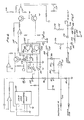
- FIG. 2 illustrates one embodiment of the detector 20 in some detail.
- the embodiment of the detector 20 shown in Figure 2 includes a coaxial input line 70 having its housing connected to a reference potential such as ground.
- a connection is also made from the coaxial line 70 to one terminal of an impedance 71 having a suitable amount such as appoximately 50 ⁇ .
- the second terminal of the impedance 71 is common with the reference potential such as the ground 12.
- the coaxial line 70 is also connected to the anode of a diode 72 and the cathode of a diode 74.
- the cathode of the diode 72 and the anode of the diode 74 are in series with a pair of capacitances 76 and 78, the common terminals of which are connected to the reference potential such as the ground 12.
- the coaxial transmission line 70 is terminated in its characteristic impedance by the resistor 71, so the length of the transmission line is not significant.
- the radio frequency signals from the oscillator 10 pass through the coaxial line to the diodes 72 and 74. In the positive half-cycles, the signals pass through the diode 72 and charge the capacitor 76 to a positive value. In the negative half-cycles, the signals pass through the diode 74 and charge the capacitance 78. Thus, a positive voltage is produced on a line 80 and a negative voltage is produced on a line 82.
- the circuitry shown in Figure 2 operates as a full wave rectifier.
- the line 151 from the interface 150 is also introduced to an amplifier-inverter 162.
- the output of the amplifier-inverter 162 is connected to a pair of diodes 166 and 168 disposed electrically in a series relationship.
- the anode of the diode 166 is common with the output of the amplifier-inverter 162 and the cathode of the diode 166 is common with the anode of the diode 168.
- the cathode of the diode 168 is connected to a line 170.
- An inductance 172 is in series with the line 170.
- a resistance 173 is connected between the inductance 172 and voltage supply 114 providing a suitable negative voltage such as -15V.
- the inductances 161 and 172 shown in Figure 4 are also included in the circuitry of Figure 5.
- the terminal of the inductance 161 opposite the line 156 receives the alternating signals through a capacitor 174 from the oscillator 10.
- the anode of a diode 178 is common with the capacitance 174 and the inductance 161, and the cathode of the diode 178 is common with the inductance 172 and one terminal of a capacitance 176.
- the other terminal of the capacitance 176 is common with an output line 179.
- the output from the amplifier-inverter 162 is positive so that current flows through the inductor 172 ( Figures 4 and 5), the diode 186 ( Figure 5), the resistances 188 and 182, the PIN diode 180, and the inductance 161 to the amplifier-inverter 154.
- the PIN diodes 186 and 180 are conductive and PIN diode 178 is non-conductive so that the RF signal from the oscillator 10 flows through the capacitor 174, the PIN diode 180, the resistances 182 and 188, the PIN diode 186 and the capacitance 176 to the output line 179.
- the diodes 166 and 168 are included primarily to produce a voltage drop and to isolate the amplifier inverter 162.
- the circuitry shown in Figure 5 and described above is provided for the attenuator 18a in Figure 1. Similar circuitry is also provided for the attenuator 18b ( Figure 1), which provides an attenuation in the range of 0dB to 20dB. Similar circuitry is also provided for the attenuator 18c, which provides an attenuation in the range of 0dB to 20dB. As will be appreciated, the attenuators 18a, 18b and 18c can be connected in the system shown in Figure 1 in various combinations to provide an attenuation between 0dB and 50dB.
- the resistance 202 and the capacitance 204 prevent the amplifier 34 from oscillating as a result of time lags in the operation of the thermistor.
- the diode 206 and the resistor 208 ensure that the bridge circuit comprising the resistors 38, 40 and 46 and the thermistor 42 in Figure 1 are maintained at a positive potential with respect to ground.
- the cathode of the diode 228 and the anode of the diode 230 are also connected through a resistance 232 to the reference potential such as the ground 12.
- the operation of the field effect transistor switch 220 is controlled by a logic translator 234 and the operation of the switch 222 is controlled by a logic translator 236.
- the logic translators 234 and 236 respectively receive signals from lines 238 and 240.
Landscapes
- Physics & Mathematics (AREA)
- General Physics & Mathematics (AREA)
- Engineering & Computer Science (AREA)
- Power Engineering (AREA)
- Measurement Of Current Or Voltage (AREA)
- Measurement Of Resistance Or Impedance (AREA)
- Indication And Recording Devices For Special Purposes And Tariff Metering Devices (AREA)
- Amplifiers (AREA)
Claims (12)
- Vorrichtung zum Kalibrieren eines Detektors (20), um den Stromfluß, der durch ein Wechselsignal erzeugt wird, genau zu messen, enthaltend:
eine Einrichtung zum Erzeugen des Wechselsignals,
eine Referenzeinrichtung (32, 34) zum Erzeugen einer Referenzspannung, die repräsentativ für die Amplitude des Wechselsignals ist,
eine Einrichtung (16, 18a, 18b, 18c) zum Leiten des Wechselsignals zu dem Detektor (20), um die Erzeugung einer Spannung vom Detektor (20) zu erhalten,
eine Einrichtung (22, 24, 26), die auf die Spannung vom Detektor (20) reagiert, zum Erzeugen einer zweiten Spannung, die auf die Spannung vom Detektor (20) reagiert und zum Kaliebrieren des Ausgangs des Detektors (20) in Übereinstimmung mit dem Wechselsignal,
eine Fehlersignalerzeugungseinrichtung (52), die auf die Referenzspannung und die zweite Spannung reagiert, um ein Fehlersignal zu erzeugen, und
eine Einrichtung (13), die auf das Fehlersignal reagiert, zum Einstellen der Amplitude des Wechselsignals, um die Größe des Fehlersignals auf ein Minimum zu reduzieren. - Vorrichtung nach Anspruch 1, wobei die Referenzeinrichtung einen Thermistor (42) enthält.
- Vorrichtung nach Anspruch 1 oder 2, enthaltend:
eine Dämpfungseinrichtung (18a, 18b, 18c) zur Erzeugung verschiedener Dämpfungsbereiche des Wechselsignals, und
eine Einrichtung zum Einstellen der Amplitude des Wechselsignals, um eine Gleichheit zu erzeugen zwischen der Spannung vom Detektor (20) für einen Maximalwert des Wechselsignals eines bestimmten Dämpfungsbereichs und den Spannungen vom Detektor (20) für den nächsten Dämpfungsbereich für den gleichen Wert des Wechselsignals. - Vorrichtung nach Anspruch einem der Ansprüche 1 bis 3, wobei die Referenzeinrichtung eine Brücke (32) und ein variables Impedanzelement (42) in der Brücke (32) enthält und wobei das variable Impedanzelement (42) seine Eigenschaften zusammen mit der Temperatur ändert, um mit den anderen Impedanzen (38, 40, 44, 46) in der Brücke (32) zu kooperieren, um die Brücke (32) abzugleichen.
- Vorrichtung nach einem der vorangehenden Ansprüche, wobei die Referenzeinrichtung enthält:
eine Einrichtung (44), die auf ein Wechselsignal reagiert zur Erzeugung einer Impedanz, die auf einen bestimmten Wert reguliert ist, selbt bei Änderungen der Amplitude und der Frequenz des Wechselsignals. - Vorrichtung nach Anspruch 3, oder einem, der davon abhängigen Ansprüche enthaltend:
eine Datenverarbeitungseinrichtung (24), die auf das Signal vom Detektor (20) reagiert, zum Kalibirieren des Ausgangs des Detektors (20), um eine Korrespondenz der Anzeige vom Detektor (20) für den Maximalwert des Wechselsignals von jedem Dämpfungsbereich und dem Minimalwert des Wechselsignals des nächsten Dämpfungsbereichs zu erzeugen. - Vorrichtung nach Anspruch 6, enthaltend:
eine Datenverarbeitungseinrichtung (24), die durch das Wechselsignal betrieben wird, um den Ausgang vom Detektor (20) einzustellen, um die Erkennung durch den Detektor (20) auf den gleichen Wert für einen Maximalwert in jedem Dämpfungsbereich und einen gleichen Wert in dem nächsten Dämpfungsbereich zu kalibrieren. - Vorrichtung nach einem der Ansprüche 6 oder 7, wobei A/D-Wandlereinrichtungen (22) zwischen den Detektor (20) und die Datenverarbeitungseinrichtung (24) geschaltet sind, um den Analogwert von dem Detektor (20) in ein digitales Signal umzuwandeln zur Zuführung zur Datenverarbeitungseinrichtung (24), und wobei D/A-Wandlereinrichtungen (26) zwischen der Datenverarbeitungseinrichtung (24) und die Fehlersignalerzeugungseinrichtung (52) geschaltet sind, um das digitale Signal von der Datenverarbeitungseinrichtung (24) in ein analoges Signal zur Zuführung zu der Fehlersignalerzeugungseinrichtung (52) umzuwandeln.
- Vorrichtung nach einem der vorangehenden Ansprüche, wobei die Fehlersignalerzeugungseinrichtung einen Operationsverstärker (52) enthält und wobei Tiefpassfiltereinrichtungen (14), die auf das Wechselsignal reagieren, vorgesehen sind, um nur die Grundfrequenz des Wechselsignals an den Detektor (20) weiterzuleiten.
- Vorrichtung nach Anspruch 3, oder einem davon abhängigen Anspruch, wobei Einrichtungen, die auf die Amplitude, die durch den Detektor (20) erkannt wird, vorgesehen sind zum Erzeugen einer Tabelle in der Datenverarbeitungseinrichtung (24), um den Stromfluß anzuzeigen, der durch das Wechselsignal erzeugt wird.
- Vorrichtung nach einem der Ansprüche 1 bis 10, wobei die Fehlersignalerzeugungseinrichtung (52) eine Einrichtung zur Erzeugung eines Referenzpotentials enthält, und daß diese Fehlersignalerzeugungseinrichtung (52) ein Fehlersignal erzeugt, das eine Kombination aus der Referenz- und zweiten Spannung und dieses Referenzpotentials ist.
- Vorrichtung nach Anspruch 4, oder einem der davon abhängigen Ansprüche, wobei die Brückenschaltung (32) abgegelichen ist, wenn die variable Impedanz (42) einen bestimmten Wert hat.
Applications Claiming Priority (2)
| Application Number | Priority Date | Filing Date | Title |
|---|---|---|---|
| US06/738,964 US4794325A (en) | 1985-05-29 | 1985-05-29 | Calibrated power detector |
| US738964 | 1985-05-29 |
Publications (3)
| Publication Number | Publication Date |
|---|---|
| EP0210373A2 EP0210373A2 (de) | 1987-02-04 |
| EP0210373A3 EP0210373A3 (en) | 1989-06-07 |
| EP0210373B1 true EP0210373B1 (de) | 1992-09-09 |
Family
ID=24970240
Family Applications (1)
| Application Number | Title | Priority Date | Filing Date |
|---|---|---|---|
| EP86107282A Expired EP0210373B1 (de) | 1985-05-29 | 1986-05-28 | Kalibrierter Stromdetektor |
Country Status (5)
| Country | Link |
|---|---|
| US (1) | US4794325A (de) |
| EP (1) | EP0210373B1 (de) |
| JP (1) | JPS61277069A (de) |
| CA (1) | CA1249631A (de) |
| DE (1) | DE3686680T2 (de) |
Families Citing this family (29)
| Publication number | Priority date | Publication date | Assignee | Title |
|---|---|---|---|---|
| US5365768A (en) * | 1989-07-20 | 1994-11-22 | Hitachi, Ltd. | Sensor |
| FR2699285B1 (fr) * | 1992-12-11 | 1995-01-06 | Thomson Csf Semiconducteurs | Dispositif de détection de puissance sur la sortie d'un circuit électronique. |
| US6407540B1 (en) * | 1999-04-09 | 2002-06-18 | Agilent Technologies, Inc. | Switched attenuator diode microwave power sensor |
| US7317902B2 (en) * | 2001-06-28 | 2008-01-08 | Harris Corporation | Successive log video pad power detector and method |
| US20090067351A1 (en) * | 2007-09-07 | 2009-03-12 | Andreas Wiesbauer | Power Detector Radio Frequency Multiplexer |
| US9534962B2 (en) * | 2010-07-19 | 2017-01-03 | Mediatek Inc. | Temperature measurement devices |
| US10257729B2 (en) | 2013-03-15 | 2019-04-09 | DGS Global Systems, Inc. | Systems, methods, and devices having databases for electronic spectrum management |
| US9078162B2 (en) | 2013-03-15 | 2015-07-07 | DGS Global Systems, Inc. | Systems, methods, and devices for electronic spectrum management |
| US12256233B2 (en) | 2013-03-15 | 2025-03-18 | Digital Global Systems, Inc. | Systems and methods for automated financial settlements for dynamic spectrum sharing |
| US10244504B2 (en) | 2013-03-15 | 2019-03-26 | DGS Global Systems, Inc. | Systems, methods, and devices for geolocation with deployable large scale arrays |
| US10237770B2 (en) | 2013-03-15 | 2019-03-19 | DGS Global Systems, Inc. | Systems, methods, and devices having databases and automated reports for electronic spectrum management |
| US10299149B2 (en) | 2013-03-15 | 2019-05-21 | DGS Global Systems, Inc. | Systems, methods, and devices for electronic spectrum management |
| US10257728B2 (en) | 2013-03-15 | 2019-04-09 | DGS Global Systems, Inc. | Systems, methods, and devices for electronic spectrum management |
| US10231206B2 (en) | 2013-03-15 | 2019-03-12 | DGS Global Systems, Inc. | Systems, methods, and devices for electronic spectrum management for identifying signal-emitting devices |
| US10271233B2 (en) | 2013-03-15 | 2019-04-23 | DGS Global Systems, Inc. | Systems, methods, and devices for automatic signal detection with temporal feature extraction within a spectrum |
| US10219163B2 (en) | 2013-03-15 | 2019-02-26 | DGS Global Systems, Inc. | Systems, methods, and devices for electronic spectrum management |
| US11646918B2 (en) | 2013-03-15 | 2023-05-09 | Digital Global Systems, Inc. | Systems, methods, and devices for electronic spectrum management for identifying open space |
| US10257727B2 (en) | 2013-03-15 | 2019-04-09 | DGS Global Systems, Inc. | Systems methods, and devices having databases and automated reports for electronic spectrum management |
| US12356206B2 (en) | 2013-03-15 | 2025-07-08 | Digital Global Systems, Inc. | Systems and methods for automated financial settlements for dynamic spectrum sharing |
| CN103558578B (zh) * | 2013-10-30 | 2017-11-21 | 国家电网公司 | 一种电子式电能表用热敏电阻检验系统及其方法 |
| US9246530B1 (en) * | 2014-12-31 | 2016-01-26 | Texas Instruments Incorporated | Built-in test system and method |
| US12205477B2 (en) | 2017-01-23 | 2025-01-21 | Digital Global Systems, Inc. | Unmanned vehicle recognition and threat management |
| US10700794B2 (en) | 2017-01-23 | 2020-06-30 | Digital Global Systems, Inc. | Systems, methods, and devices for automatic signal detection based on power distribution by frequency over time within an electromagnetic spectrum |
| US10529241B2 (en) | 2017-01-23 | 2020-01-07 | Digital Global Systems, Inc. | Unmanned vehicle recognition and threat management |
| US10459020B2 (en) | 2017-01-23 | 2019-10-29 | DGS Global Systems, Inc. | Systems, methods, and devices for automatic signal detection based on power distribution by frequency over time within a spectrum |
| US12183213B1 (en) | 2017-01-23 | 2024-12-31 | Digital Global Systems, Inc. | Unmanned vehicle recognition and threat management |
| US10498951B2 (en) | 2017-01-23 | 2019-12-03 | Digital Global Systems, Inc. | Systems, methods, and devices for unmanned vehicle detection |
| US10943461B2 (en) | 2018-08-24 | 2021-03-09 | Digital Global Systems, Inc. | Systems, methods, and devices for automatic signal detection based on power distribution by frequency over time |
| CN116299126B (zh) * | 2023-05-16 | 2023-08-29 | 上海安其威微电子科技有限公司 | 校准电路、系统、方法、控制单元、存储介质、程序产品 |
Family Cites Families (6)
| Publication number | Priority date | Publication date | Assignee | Title |
|---|---|---|---|---|
| US3653037A (en) * | 1969-12-31 | 1972-03-28 | Ibm | Apparatus and a method for automatically testing a system which receives an analog input signal |
| US4063447A (en) * | 1977-03-14 | 1977-12-20 | Honeywell, Inc. | Bridge circuit with drift compensation |
| US4700128A (en) * | 1980-11-13 | 1987-10-13 | Levonius Jr Carl G | Electronic calibrator |
| US4546313A (en) * | 1983-03-14 | 1985-10-08 | The United States Of America As Represented By The United States Department Of Energy | Peak power ratio generator |
| DD214939A1 (de) * | 1983-05-04 | 1984-10-24 | Robotron Bueromasch | Frequenzdiskriminator |
| US4692696A (en) * | 1985-07-29 | 1987-09-08 | Gte Communication Systems Corporation | Method for adjusting and testing current sensors |
-
1985
- 1985-05-29 US US06/738,964 patent/US4794325A/en not_active Expired - Lifetime
-
1986
- 1986-05-12 CA CA000508846A patent/CA1249631A/en not_active Expired
- 1986-05-28 DE DE8686107282T patent/DE3686680T2/de not_active Expired - Fee Related
- 1986-05-28 EP EP86107282A patent/EP0210373B1/de not_active Expired
- 1986-05-29 JP JP61122388A patent/JPS61277069A/ja active Pending
Also Published As
| Publication number | Publication date |
|---|---|
| CA1249631A (en) | 1989-01-31 |
| DE3686680T2 (de) | 1993-02-11 |
| DE3686680D1 (de) | 1992-10-15 |
| EP0210373A3 (en) | 1989-06-07 |
| US4794325A (en) | 1988-12-27 |
| JPS61277069A (ja) | 1986-12-08 |
| EP0210373A2 (de) | 1987-02-04 |
Similar Documents
| Publication | Publication Date | Title |
|---|---|---|
| EP0210373B1 (de) | Kalibrierter Stromdetektor | |
| US3919644A (en) | Automatic antenna coupler utilizing system for measuring the real part of the complex impedance or admittance presented by an antenna or other network | |
| US4794343A (en) | Method and apparatus for calibrating and equalizing a multi-channel automatic gain control amplifier | |
| US5061900A (en) | Self-zeroing amplifier | |
| US4977366A (en) | High frequency power sensing device | |
| US4236126A (en) | Variable RF attenuator | |
| US4727337A (en) | Protection circuit for RF power amplifiers | |
| US4970456A (en) | Temperature compensated power detector | |
| US4857827A (en) | Electronic load for testing transformers | |
| US4447783A (en) | Programmable RF power regulator (stabilizer) | |
| US4000463A (en) | Direct-reading decibel meter | |
| EP0035403A1 (de) | Spannungsmessinstrument und Vorverstärker dafür | |
| US4217506A (en) | Level selective a-c monitoring circuit | |
| US4644306A (en) | Programmable electronic synthesized capacitance | |
| US4333023A (en) | Temperature-stabilized logarithmic converter | |
| US3217247A (en) | System for measurement of attenuation taken directly in decibels at radio frequencies utilizing logarithmic circuits | |
| US3423675A (en) | Measuring system for two and four terminal networks | |
| US4733173A (en) | Electronic component measurement apparatus | |
| US4249127A (en) | Standing wave ratio measuring system | |
| US2776406A (en) | Power measuring instrument and method | |
| EP0456921A1 (de) | Dämpfungsglied | |
| US4145661A (en) | Precision measuring amplifier | |
| US2625589A (en) | System for measuring phase and gain | |
| US4797774A (en) | Signal conditioning circuit | |
| US3142017A (en) | Precision direct current substitution bridge for measuring r. f. values |
Legal Events
| Date | Code | Title | Description |
|---|---|---|---|
| PUAI | Public reference made under article 153(3) epc to a published international application that has entered the european phase |
Free format text: ORIGINAL CODE: 0009012 |
|
| AK | Designated contracting states |
Kind code of ref document: A2 Designated state(s): DE FR GB |
|
| PUAL | Search report despatched |
Free format text: ORIGINAL CODE: 0009013 |
|
| AK | Designated contracting states |
Kind code of ref document: A3 Designated state(s): DE FR GB |
|
| RHK1 | Main classification (correction) |
Ipc: G01R 35/00 |
|
| 17P | Request for examination filed |
Effective date: 19891205 |
|
| 17Q | First examination report despatched |
Effective date: 19900918 |
|
| GRAA | (expected) grant |
Free format text: ORIGINAL CODE: 0009210 |
|
| AK | Designated contracting states |
Kind code of ref document: B1 Designated state(s): DE FR GB |
|
| REF | Corresponds to: |
Ref document number: 3686680 Country of ref document: DE Date of ref document: 19921015 |
|
| ET | Fr: translation filed | ||
| PLBE | No opposition filed within time limit |
Free format text: ORIGINAL CODE: 0009261 |
|
| STAA | Information on the status of an ep patent application or granted ep patent |
Free format text: STATUS: NO OPPOSITION FILED WITHIN TIME LIMIT |
|
| 26N | No opposition filed | ||
| REG | Reference to a national code |
Ref country code: GB Ref legal event code: 732E |
|
| REG | Reference to a national code |
Ref country code: FR Ref legal event code: TP |
|
| PGFP | Annual fee paid to national office [announced via postgrant information from national office to epo] |
Ref country code: GB Payment date: 20010808 Year of fee payment: 16 |
|
| PGFP | Annual fee paid to national office [announced via postgrant information from national office to epo] |
Ref country code: FR Payment date: 20010810 Year of fee payment: 16 |
|
| PGFP | Annual fee paid to national office [announced via postgrant information from national office to epo] |
Ref country code: DE Payment date: 20010813 Year of fee payment: 16 |
|
| REG | Reference to a national code |
Ref country code: GB Ref legal event code: IF02 |
|
| PG25 | Lapsed in a contracting state [announced via postgrant information from national office to epo] |
Ref country code: GB Free format text: LAPSE BECAUSE OF NON-PAYMENT OF DUE FEES Effective date: 20020528 |
|
| PG25 | Lapsed in a contracting state [announced via postgrant information from national office to epo] |
Ref country code: DE Free format text: LAPSE BECAUSE OF NON-PAYMENT OF DUE FEES Effective date: 20021203 |
|
| GBPC | Gb: european patent ceased through non-payment of renewal fee |
Effective date: 20020528 |
|
| PG25 | Lapsed in a contracting state [announced via postgrant information from national office to epo] |
Ref country code: FR Free format text: LAPSE BECAUSE OF NON-PAYMENT OF DUE FEES Effective date: 20030331 |
|
| REG | Reference to a national code |
Ref country code: FR Ref legal event code: ST |
|
| PG25 | Lapsed in a contracting state [announced via postgrant information from national office to epo] |
Ref country code: FR Free format text: LAPSE BECAUSE OF NON-PAYMENT OF DUE FEES Effective date: 20020531 |