EP0210529B1 - Circuit d'interface pour une unité à disquettes - Google Patents
Circuit d'interface pour une unité à disquettes Download PDFInfo
- Publication number
- EP0210529B1 EP0210529B1 EP86109659A EP86109659A EP0210529B1 EP 0210529 B1 EP0210529 B1 EP 0210529B1 EP 86109659 A EP86109659 A EP 86109659A EP 86109659 A EP86109659 A EP 86109659A EP 0210529 B1 EP0210529 B1 EP 0210529B1
- Authority
- EP
- European Patent Office
- Prior art keywords
- signal
- gate
- window
- kbps
- mode
- Prior art date
- Legal status (The legal status is an assumption and is not a legal conclusion. Google has not performed a legal analysis and makes no representation as to the accuracy of the status listed.)
- Expired - Lifetime
Links
Images


Classifications
-
- G—PHYSICS
- G06—COMPUTING OR CALCULATING; COUNTING
- G06F—ELECTRIC DIGITAL DATA PROCESSING
- G06F13/00—Interconnection of, or transfer of information or other signals between, memories, input/output devices or central processing units
-
- G—PHYSICS
- G06—COMPUTING OR CALCULATING; COUNTING
- G06F—ELECTRIC DIGITAL DATA PROCESSING
- G06F3/00—Input arrangements for transferring data to be processed into a form capable of being handled by the computer; Output arrangements for transferring data from processing unit to output unit, e.g. interface arrangements
- G06F3/06—Digital input from, or digital output to, record carriers, e.g. RAID, emulated record carriers or networked record carriers
- G06F3/0601—Interfaces specially adapted for storage systems
-
- G—PHYSICS
- G11—INFORMATION STORAGE
- G11B—INFORMATION STORAGE BASED ON RELATIVE MOVEMENT BETWEEN RECORD CARRIER AND TRANSDUCER
- G11B20/00—Signal processing not specific to the method of recording or reproducing; Circuits therefor
- G11B20/10—Digital recording or reproducing
-
- G—PHYSICS
- G11—INFORMATION STORAGE
- G11B—INFORMATION STORAGE BASED ON RELATIVE MOVEMENT BETWEEN RECORD CARRIER AND TRANSDUCER
- G11B5/00—Recording by magnetisation or demagnetisation of a record carrier; Reproducing by magnetic means; Record carriers therefor
- G11B5/012—Recording on, or reproducing or erasing from, magnetic disks
- G11B5/016—Recording on, or reproducing or erasing from, magnetic disks using magnetic foils
-
- G—PHYSICS
- G11—INFORMATION STORAGE
- G11B—INFORMATION STORAGE BASED ON RELATIVE MOVEMENT BETWEEN RECORD CARRIER AND TRANSDUCER
- G11B5/00—Recording by magnetisation or demagnetisation of a record carrier; Reproducing by magnetic means; Record carriers therefor
- G11B5/02—Recording, reproducing, or erasing methods; Read, write or erase circuits therefor
- G11B5/09—Digital recording
-
- G—PHYSICS
- G06—COMPUTING OR CALCULATING; COUNTING
- G06F—ELECTRIC DIGITAL DATA PROCESSING
- G06F3/00—Input arrangements for transferring data to be processed into a form capable of being handled by the computer; Output arrangements for transferring data from processing unit to output unit, e.g. interface arrangements
- G06F3/06—Digital input from, or digital output to, record carriers, e.g. RAID, emulated record carriers or networked record carriers
- G06F3/0601—Interfaces specially adapted for storage systems
- G06F3/0668—Interfaces specially adapted for storage systems adopting a particular infrastructure
- G06F3/0671—In-line storage system
- G06F3/0673—Single storage device
Definitions
- the present invention relates to a floppy disk drive interface circuit and especially to a floppy disk drive (hereinafter referred to as FDD) window signal gate circuit used in an FDD interface mechanism in which the data transfer rate of an FDD is unknown.
- FDD floppy disk drive
- a recording medium having either double-sided, double-density, double tracks (2DD type) or double-sided, double-density tracks (2D type).
- the recording medium is driven at 300 rpm by a spindle motor.
- the data transfer rate in the read operation is 250 kbps.
- a recording medium having double-sided, high-density, double tracks (2HD type) has also been developed.
- the rotational frequency of the spindle motor for an FDD is 360 rpm, and the data transfer rate in the read operation is 500 kbps.
- a disk drive for 2HD type medium can drive a recording medium of 2DD or 2D type. Since the rotational frequency of the spindle motor used in this disk drive is 360 rpm, the data transfer rate is 300 kbps.
- the rotational frequency of the spindle motor is switched between 360 and 300 rpm.
- an extra wait time must be required for switching the rotational frequency of the spindle motor.
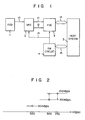
- a conventional FDD interface circuit consists of variable frequency oscillator (VFO) 2, floppy disk controller (FDC) 3, and switching circuit 4, as shown in Fig. 1.
- VFO variable frequency oscillator
- FDC floppy disk controller
- Switching circuit 4 supplies a signal (250 kbps, 300 kbps, or 500 kbps) for switching the data transfer rate to VFO 2 and FDC 3.
- Host system 5 reads data from FDD 1.
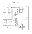
- Host system 5 and FDC 3 are connected by bus 14, and host system 5 and switching circuit 4 are connected by bus 15. Even if the data transfer rate of data 10 slightly fluctuates by VFO 2, FDC 3 can correctly read ID information and data. Therefore, the data transfer rate has some allowance in all of the 250 kbps, 300 kbps, and 500 kbps modes. This allowance is called a capture range. In the 250 kbps and 300 kbps modes, the center frequencies are close to each other. Therefore, if the capture range of VFO 2 is wide, the transfer rates overlap as shown in Fig. 2. When this occurs, in the 300 kbps mode, data written in the 250 kbps mode is read as indicated by the broken lines in Fig. 2. Conversely, in the 250 kbps mode, data written in the 300 kb p s mode is read. Therefore, host system 5 cannot correctly identify the mode.
- Prior art document DE-A-3133175 discloses a phase control circuit for synchronizing input signals with reference signals.
- a circuit stage compares two input signals and delivers an output signal which is fed back to a variable frequency oscillator. If the comparison result does not satisfy a predetermined condition, the oscillation frequency of the variable frequency oscillator is set to a fixed value.
- the phase control circuit After receipt of read data, the phase control circuit starts a tracking operation: It compares a period of read data with a predetermined width, and if the period is within the predetermined width, the circuit makes the variable frequency oscillator to track the read data. On the contrary, if the period excesses the predetermined width, the variable frequency oscillator ceases to track read data, and outputs a fixed frequency.
- the present invention provides a floppy disk drive interface circuit as defined in the claim.
- Fig. 3 is a block diagram of an FDD interface circuit using FDD window signal gate circuit 33 according to the present invention.
- the same reference numerals denote the same parts as in Fig. 1.
- gate circuit 33 indicated by the dotted line is included in the FDD interface circuit.
- Counter/selector 21 receives a basic clock signal 30 from oscillator 20, counts the pulse width for time intervals T1 and T2 in Figs. 5C through 5F, and supplies corresponding window gate signal 31 to gate circuit 22.
- Time interval T1 corresponds to a count period of counter/selector 21 in the 250 kbps mode
- time interval T2 corresponds to the count period of counter/selector 21 in the 300 kbps mode.
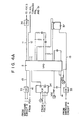
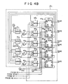
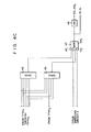
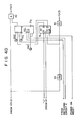
- Figs. 4A through 4D are circuit diagrams of the FDD interface circuit shown in Fig. 4.
- Fig. 4A shows a peripheral portion of VFO 2 in Fig. 3.
- Mode switching signal 13 is supplied from circuit 4 to VFO 2 through OR gate 33.
- Raw read data 10 is supplied from FDD 1 to VFO 2.
- a control signal for controlling VFO 2 is supplied from FDC 3 through flip-flop (F/F) 34.
- Switching signal 13 is supplied to element 37.
- Element 37 shifts the center frequency of VFO 2.
- VFO 2 supplies read data signal 11 to FDC 3 through inverter 36, and also supplies window signal 12 to flip-flops 44, to 44 5 of counter/selector 21.
- counter/selector 21 consists of NAND gates 41 1 to 41 4 , Exclusive-OR gates 42 1 to 42 4 , AND-NOR gates 43 1 to 43 5 , and flip-flops 44, to 44 5 .
- Window signal 12 is supplied as a reset signal from VFO 2 to clear terminals (CLR) of flip-flops 44, to 44 5 .
- Clock input terminals CK of flip-flops 44, to 44 5 receive a 16-MHz basic clock signal from oscillator 20.
- Respective flip-flops 44, to 44 5 receive at their D terminals the outputs from corresponding AND-NOR gates 43, to 43 5 .
- the Q output from flip-flop 44 is fed back to NAND gates 41, to 41 4 ; the Q output from flip-flop 44 2 , to NAND gates 41 2 to 41 4 ; the Q output from flip-flop 44 3 , to NAND gates 41 3 and 41 4 ; and the Q output from flip-flop 44 4 , to NAND gate 41 4 .
- Outputs from AND-NOR gate 47 and inverter 48 (to be described later) in Fig. 4C are supplied to AND-NOR gates 43 1 to 43 5 .
- NAND gate 45 The Q outputs from flip-flops 44, to 44 5 are supplied to NAND gate 45 in Fig. 4C, and the Q outputs from flip-flops 44 1 , 44 2 , 44 4 , and 44 5 are supplied to NAND gate 46.
- NAND gate 46 also receives Q output from flip-flop 44 3 .
- NAND gate 45 When 5-bit counter 21, in Fig. 4B has a full count, i.e., a count of "32" corresponding to 2 ⁇ sec when the frequency of the basic clock signal is 16 MHz, NAND gate 45 produces an active signal. When counter 21, counts to "27”, i.e., 1.7 ⁇ sec, NAND gate 46 generates an active signal.
- Outputs from NAND gates 45 and 46 are supplied to AND-NOR gate 47.
- Switching signal 13 from switching circuit 4 is supplied to gate 47.
- An output from gate 47 is supplied to the D input terminal of flip-flop 51 in Fig. 4D and to AND-NOR gates 43, to 43 5 (Fig. 4B) through inverter 48.
- Flip-flop 51 holds the previous count of counter 21, in Fig. 4B.
- Window signal 12 from VFO 2 is supplied to clock input terminal (CK) of flip-flop 51 through inverter 52.
- Window signal 12 from VFO 2 is also supplied to FDC 3 through AND gate 49.
- the Q and Q outputs from flip-flop 51 are supplied to selector 21 2 .
- Selector 21 2 also receives, selection data, i.e., mode switching signal 13, from switching circuit 4.
- the Q output signal from flip-flop 51 goes to high level (logic "1") when the pulse width of the input window pulse is longer than that counted by counter 21, in Fig. 41B, and the Q output signal thereof rises to high level (logic "1") when it is shorter.
- the Q output signal from flip-flop 51 is supplied to input terminal 2 of selector 21 2 .
- the Q output signal from flip-flop 51 is supplied to input terminal 1 of selector 21 2 .
- the value of flip-flop 51 is held until a window pulse of a different period is received.
- mode switching signal 13 from switching circuit 4 under the control of host system 5.
- window pulse 12 in Fig. 5A is output from VFO 2.
- the window pulse in this case has a period of about 4 ⁇ sec. Therefore, the significant level (active level) interval of window pulse 12 is about 2 ⁇ sec.
- the counter shown in Fig. 4B is cleared when window pulse 12 goes to logic "1", and is clocked by and counts the basic clock signal (16 MHz) from oscillator 20.
- a logic signal from NAND gate 46 is set at one input of AND gate 47 2 .
- a logic "0" signal is applied to the other input of AND gate 47 2 . Since the 250 kbps mode has been selected, a logic "1" signal from circuit 4 is applied to AND gate 47 1 , and a logic "0" signal is applied to AND gate 47 2 .
- AND gate 47 2 receives "0" and “0” signals or "0" and “1” signals, and always outputs a "0". Therefore, the output from NOR gate 47 3 depends only on an output from AND gate 47 1 . In other words, the output from NOR gate 47 3 is a NOT of the output from AND gate 47 1 .
- NAND gate 45 When the count of counter 21, reaches "32", i.e., when counter 21, counts 2.0 ⁇ sec, NAND gate 45 receives all bit “1” inputs and outputs a logic "0" signal. Therefore, AND gate 47, receives "0" and "1" signals.
- NAND gate 46 when counter 21, counts up to 1.7 ⁇ sec, NAND gate 46 generates a logic "0" signal. A logic “1” signal is supplied to AND gate 47 1 , and AND gate 47 2 receives a logic “0” signal from NAND gate 46 and a logic “1” signal representing the 300 kbps mode from switching circuit 4. NOR gate 47 3 thus generates a logic "1” signal. A logic “1” signal is set in flip-flop 51, and a Q output signal of logic "0" is applied to input terminal 3 which has been selected in the 300 kbps mode. Since a logic "0" signal is applied to AND gate 22, the 250 kbps window pulse is blocked.
- selector 21 2 selects the level (logic "1") at input terminal 0 regardless of the output from F/F 51. Therefore, AND gate 22 gates all pulses. This is because 500 kbps and 300 kbps are sufficiently separated, and the capture ranges do not overlap.
- Figs. 7A through 7D show the outputs from selector 21 2 and AND gate 22 when 250 kbps and 300 kbps window pulses are both input.
- Fig. 7B shows the output from selector 21 2 in the 250 kbps mode
- Fig. 7C shows the output from AND gate 22 in the 250 kbps mode.
- Fig. 7D shows the output from selector 21 2 in the 300 kbps mode
- Fig. 7E shows the output from AND gate 22 in the 300 kbps mode.
- host system 5 correctly identifies the data transfer rate of FDD 1.
- the capture range will not be so wide that 300 kbps data is read in the 250 kbps mode, or vice versa (indicated by the dotted lines in Fig. 6).
- host system 5 can correctly identify the mode. If a digital counter is used as a circuit for measuring the pulse width of a window pulse, it requires no adjustment and can offer higher precision than an arrangement using an analog one-shot circuit.
- the margin is wider than the case wherein raw read data is used.
Landscapes
- Engineering & Computer Science (AREA)
- Theoretical Computer Science (AREA)
- Physics & Mathematics (AREA)
- General Engineering & Computer Science (AREA)
- General Physics & Mathematics (AREA)
- Human Computer Interaction (AREA)
- Signal Processing (AREA)
- Signal Processing For Digital Recording And Reproducing (AREA)
- Stabilization Of Oscillater, Synchronisation, Frequency Synthesizers (AREA)
Claims (1)
- Circuit d'interface de lecteur de disque souple dans un système capable de traiter plusieurs vitesses de transfert de données, comprenant un lecteur de disque souple (1); un oscillateur à fréquence variable (VFO) (2) destiné à émettre un signal de données de lecture et un signal de fenêtre en verrouillant un dispositif générateur d'horloge de base produisant un signal d'horloge de base sur une impulsion de données lues produites par ledit lecteur de disque souple; et un dispositif (4) destiné à émettre un signal de mode représentant un ensemble de vitesses de transfert de données du signal de données de lecture, caractérisé en ce qu'il comporte également:un dispositif (211) destiné à recevoir le signal d'horloge de base provenant du dispositif générateur d'horloge de base et le signal de fenêtre provenant dudit oscillateur à fréquence variable (2) et mesurant la durée d'impulsion du signal de fenêtre;un dispositif (figures 4C et 4D) connecté audit dispositif de mesure de durée d'impulsion et audit dispositif générateur de signal de mode pour produire un signal de porte de fenêtre actif quand la durée d'impulsion mesurée ne correspond pas à la durée d'impulsion prédéterminée d'un signal de fenêtre produit en correspondance avec la vitesse de transfert de données attendue comme l'indique le signal de mode; etun dispositif à portes (22) connecté audit dispositif générateur de signal de porte de fenêtre et audit oscillateur à fréquence variable (2) pour aiguiller le signal de fenêtre en réponse au signal de fenêtre actif provenant dudit oscillateur à fréquence variable en fonction du signal de porte de fenêtre.
Applications Claiming Priority (2)
| Application Number | Priority Date | Filing Date | Title |
|---|---|---|---|
| JP60167237A JPH0650591B2 (ja) | 1985-07-29 | 1985-07-29 | Fddウインドウゲ−ト回路 |
| JP167237/85 | 1985-07-29 |
Publications (3)
| Publication Number | Publication Date |
|---|---|
| EP0210529A2 EP0210529A2 (fr) | 1987-02-04 |
| EP0210529A3 EP0210529A3 (en) | 1988-08-10 |
| EP0210529B1 true EP0210529B1 (fr) | 1990-09-19 |
Family
ID=15845998
Family Applications (1)
| Application Number | Title | Priority Date | Filing Date |
|---|---|---|---|
| EP86109659A Expired - Lifetime EP0210529B1 (fr) | 1985-07-29 | 1986-07-14 | Circuit d'interface pour une unité à disquettes |
Country Status (5)
| Country | Link |
|---|---|
| US (1) | US4724493A (fr) |
| EP (1) | EP0210529B1 (fr) |
| JP (1) | JPH0650591B2 (fr) |
| KR (1) | KR900002968B1 (fr) |
| DE (1) | DE3674286D1 (fr) |
Families Citing this family (11)
| Publication number | Priority date | Publication date | Assignee | Title |
|---|---|---|---|---|
| JPS63138506A (ja) * | 1986-11-29 | 1988-06-10 | Toshiba Corp | フロツピ−デイスク装置のデ−タ再生回路 |
| JPS6472304A (en) * | 1987-09-14 | 1989-03-17 | Toshiba Corp | Magnetic head device for floppy disk device |
| US4935941A (en) * | 1988-03-30 | 1990-06-19 | Konica Corporation | Multiple frequency data recovery system |
| US5111486A (en) * | 1989-03-15 | 1992-05-05 | Motorola, Inc. | Bit synchronizer |
| JPH03144720A (ja) * | 1989-10-31 | 1991-06-20 | Toshiba Corp | Fddの識別方法ならびにfddの認識回路 |
| JPH05234273A (ja) * | 1990-11-30 | 1993-09-10 | Hitachi Ltd | 信号波形の評価装置および磁気ディスク装置 |
| US5301300A (en) * | 1991-02-14 | 1994-04-05 | Advanced Micro Devices, Inc. | Floppy disk drive controller with improved density select |
| JP2536984B2 (ja) * | 1991-09-26 | 1996-09-25 | インターナショナル・ビジネス・マシーンズ・コーポレイション | 周辺装置の制御方法、フロッピ・ディスク装置の制御方法、周辺装置、フロッピ・ディスク装置、及び、デ―タ処理システム |
| US5761699A (en) * | 1993-08-20 | 1998-06-02 | Teac Corporation | System for adapting a computer system to different types of data storage disks for interchangeable use with a disk drive |
| US6449686B1 (en) | 1997-03-06 | 2002-09-10 | Micron Technology, Inc. | Method and apparatus for determining removable magnetic media types in a computer after detection of a read error condition |
| US7424120B2 (en) * | 2003-08-06 | 2008-09-09 | Avago Technologies General Ip Pte Ltd | Method and apparatus for volume control |
Family Cites Families (4)
| Publication number | Priority date | Publication date | Assignee | Title |
|---|---|---|---|---|
| JPS5720052A (en) * | 1980-07-11 | 1982-02-02 | Toshiba Corp | Input data synchronizing circuit |
| DE3133175A1 (de) * | 1981-08-21 | 1983-03-03 | Siemens AG, 1000 Berlin und 8000 München | Phasenregelkreis |
| US4462051A (en) * | 1982-04-02 | 1984-07-24 | Ampex Corporation | Demodulator for an asynchronous binary signal |
| JPS59207068A (ja) * | 1983-05-10 | 1984-11-24 | Panafacom Ltd | フロツピイデイスク装置 |
-
1985
- 1985-07-29 JP JP60167237A patent/JPH0650591B2/ja not_active Expired - Lifetime
-
1986
- 1986-07-11 US US06/884,639 patent/US4724493A/en not_active Expired - Fee Related
- 1986-07-14 EP EP86109659A patent/EP0210529B1/fr not_active Expired - Lifetime
- 1986-07-14 DE DE8686109659T patent/DE3674286D1/de not_active Expired - Lifetime
- 1986-07-28 KR KR8606138A patent/KR900002968B1/ko not_active Expired
Also Published As
| Publication number | Publication date |
|---|---|
| JPS6228975A (ja) | 1987-02-06 |
| KR900002968B1 (en) | 1990-05-03 |
| KR870001521A (ko) | 1987-03-14 |
| EP0210529A2 (fr) | 1987-02-04 |
| DE3674286D1 (de) | 1990-10-25 |
| JPH0650591B2 (ja) | 1994-06-29 |
| EP0210529A3 (en) | 1988-08-10 |
| US4724493A (en) | 1988-02-09 |
Similar Documents
| Publication | Publication Date | Title |
|---|---|---|
| USRE39809E1 (en) | Hard sectoring circuit and method for a rotating disk data storage device | |
| US4144583A (en) | Secondary storage facility with means for monitoring error conditions | |
| US4183084A (en) | Secondary storage facility with serial transfer of control messages | |
| US4425646A (en) | Input data synchronizing circuit | |
| EP0517483B1 (fr) | Décodeur de données RLL de marques d'adresse tolérant des erreurs | |
| US4210959A (en) | Controller for magnetic disc, recorder, or the like | |
| US4642759A (en) | Bubble memory disk emulation system | |
| EP0210529B1 (fr) | Circuit d'interface pour une unité à disquettes | |
| US4101969A (en) | Secondary storage facility with means for monitoring sector pulses | |
| EP0270057B1 (fr) | Appareil pour reproduire des données à partir d'un support d'enregistrement magnétique | |
| JPH04507474A (ja) | ゾーン密度セクターカウンタ | |
| JPS59207068A (ja) | フロツピイデイスク装置 | |
| US4933939A (en) | Method and apparatus for error measurement and reduction in a mass storage device memory system | |
| EP0686300B1 (fr) | Demarcation fiable des domaines temporels de formats fractionnes dans des lecteurs de disques d'enregistrement a asservissement incruste et donnees en zones | |
| US4672483A (en) | Information recording and reading apparatus having recording error checking circuit | |
| US4245264A (en) | Apparatus and method for digitally synchronizing the timing of a sequence of electrical output pulses in accordance with a selectable, permissably non-linear function of the timing of a sequence of electrical input pulses | |
| JPH0566676B2 (fr) | ||
| EP0404120A2 (fr) | Système de commutation de signaux de synchronisation pour la synchronisation des dispositifs de stockages externes | |
| US4173027A (en) | Write precompensation system | |
| US4141046A (en) | Floppy disc data separator for use with single density encoding | |
| US5293625A (en) | Signal selecting circuit which selectively outputs predetermined signal to host computer compatible with plurality of computer hardware types and disk drive having such signal selecting circuit | |
| EP0315295A1 (fr) | Appareil à coder et décoder des données et diviseur de fréquence en proportion 3/2 | |
| US4914369A (en) | Disc drive with improved storage capacity | |
| US4953043A (en) | Magnetic recording or reproducing apparatus with erasing capability | |
| EP0266135A2 (fr) | Appareil et méthode pour augmenter la capacité de mémoire d'une unité de mémoire à disques |
Legal Events
| Date | Code | Title | Description |
|---|---|---|---|
| PUAI | Public reference made under article 153(3) epc to a published international application that has entered the european phase |
Free format text: ORIGINAL CODE: 0009012 |
|
| 17P | Request for examination filed |
Effective date: 19860811 |
|
| AK | Designated contracting states |
Kind code of ref document: A2 Designated state(s): DE FR GB |
|
| PUAL | Search report despatched |
Free format text: ORIGINAL CODE: 0009013 |
|
| AK | Designated contracting states |
Kind code of ref document: A3 Designated state(s): DE FR GB |
|
| 17Q | First examination report despatched |
Effective date: 19881110 |
|
| GRAA | (expected) grant |
Free format text: ORIGINAL CODE: 0009210 |
|
| AK | Designated contracting states |
Kind code of ref document: B1 Designated state(s): DE FR GB |
|
| REF | Corresponds to: |
Ref document number: 3674286 Country of ref document: DE Date of ref document: 19901025 |
|
| ET | Fr: translation filed | ||
| PLBE | No opposition filed within time limit |
Free format text: ORIGINAL CODE: 0009261 |
|
| STAA | Information on the status of an ep patent application or granted ep patent |
Free format text: STATUS: NO OPPOSITION FILED WITHIN TIME LIMIT |
|
| 26N | No opposition filed | ||
| PGFP | Annual fee paid to national office [announced via postgrant information from national office to epo] |
Ref country code: GB Payment date: 19960705 Year of fee payment: 11 |
|
| PGFP | Annual fee paid to national office [announced via postgrant information from national office to epo] |
Ref country code: FR Payment date: 19960709 Year of fee payment: 11 |
|
| PGFP | Annual fee paid to national office [announced via postgrant information from national office to epo] |
Ref country code: DE Payment date: 19960722 Year of fee payment: 11 |
|
| PG25 | Lapsed in a contracting state [announced via postgrant information from national office to epo] |
Ref country code: GB Free format text: LAPSE BECAUSE OF NON-PAYMENT OF DUE FEES Effective date: 19970714 |
|
| GBPC | Gb: european patent ceased through non-payment of renewal fee |
Effective date: 19970714 |
|
| PG25 | Lapsed in a contracting state [announced via postgrant information from national office to epo] |
Ref country code: FR Free format text: LAPSE BECAUSE OF NON-PAYMENT OF DUE FEES Effective date: 19980331 |
|
| PG25 | Lapsed in a contracting state [announced via postgrant information from national office to epo] |
Ref country code: DE Free format text: LAPSE BECAUSE OF NON-PAYMENT OF DUE FEES Effective date: 19980401 |
|
| REG | Reference to a national code |
Ref country code: FR Ref legal event code: ST |