EP0210578A2 - Appareil et procédé de dépôt en continu d'isolateurs électriques - Google Patents
Appareil et procédé de dépôt en continu d'isolateurs électriques Download PDFInfo
- Publication number
- EP0210578A2 EP0210578A2 EP86110049A EP86110049A EP0210578A2 EP 0210578 A2 EP0210578 A2 EP 0210578A2 EP 86110049 A EP86110049 A EP 86110049A EP 86110049 A EP86110049 A EP 86110049A EP 0210578 A2 EP0210578 A2 EP 0210578A2
- Authority
- EP
- European Patent Office
- Prior art keywords
- chamber
- substrate
- insulator
- coupling means
- deposition
- Prior art date
- Legal status (The legal status is an assumption and is not a legal conclusion. Google has not performed a legal analysis and makes no representation as to the accuracy of the status listed.)
- Granted
Links
Images


Classifications
-
- H—ELECTRICITY
- H10—SEMICONDUCTOR DEVICES; ELECTRIC SOLID-STATE DEVICES NOT OTHERWISE PROVIDED FOR
- H10P—GENERIC PROCESSES OR APPARATUS FOR THE MANUFACTURE OR TREATMENT OF DEVICES COVERED BY CLASS H10
- H10P72/00—Handling or holding of wafers, substrates or devices during manufacture or treatment thereof
- H10P72/30—Handling or holding of wafers, substrates or devices during manufacture or treatment thereof for conveying, e.g. between different workstations
- H10P72/33—Handling or holding of wafers, substrates or devices during manufacture or treatment thereof for conveying, e.g. between different workstations into and out of processing chamber
- H10P72/3306—Horizontal transfer of a single workpiece
-
- C—CHEMISTRY; METALLURGY
- C23—COATING METALLIC MATERIAL; COATING MATERIAL WITH METALLIC MATERIAL; CHEMICAL SURFACE TREATMENT; DIFFUSION TREATMENT OF METALLIC MATERIAL; COATING BY VACUUM EVAPORATION, BY SPUTTERING, BY ION IMPLANTATION OR BY CHEMICAL VAPOUR DEPOSITION, IN GENERAL; INHIBITING CORROSION OF METALLIC MATERIAL OR INCRUSTATION IN GENERAL
- C23C—COATING METALLIC MATERIAL; COATING MATERIAL WITH METALLIC MATERIAL; SURFACE TREATMENT OF METALLIC MATERIAL BY DIFFUSION INTO THE SURFACE, BY CHEMICAL CONVERSION OR SUBSTITUTION; COATING BY VACUUM EVAPORATION, BY SPUTTERING, BY ION IMPLANTATION OR BY CHEMICAL VAPOUR DEPOSITION, IN GENERAL
- C23C16/00—Chemical coating by decomposition of gaseous compounds, without leaving reaction products of surface material in the coating, i.e. chemical vapour deposition [CVD] processes
- C23C16/44—Chemical coating by decomposition of gaseous compounds, without leaving reaction products of surface material in the coating, i.e. chemical vapour deposition [CVD] processes characterised by the method of coating
- C23C16/455—Chemical coating by decomposition of gaseous compounds, without leaving reaction products of surface material in the coating, i.e. chemical vapour deposition [CVD] processes characterised by the method of coating characterised by the method used for introducing gases into reaction chamber or for modifying gas flows in reaction chamber
-
- C—CHEMISTRY; METALLURGY
- C23—COATING METALLIC MATERIAL; COATING MATERIAL WITH METALLIC MATERIAL; CHEMICAL SURFACE TREATMENT; DIFFUSION TREATMENT OF METALLIC MATERIAL; COATING BY VACUUM EVAPORATION, BY SPUTTERING, BY ION IMPLANTATION OR BY CHEMICAL VAPOUR DEPOSITION, IN GENERAL; INHIBITING CORROSION OF METALLIC MATERIAL OR INCRUSTATION IN GENERAL
- C23C—COATING METALLIC MATERIAL; COATING MATERIAL WITH METALLIC MATERIAL; SURFACE TREATMENT OF METALLIC MATERIAL BY DIFFUSION INTO THE SURFACE, BY CHEMICAL CONVERSION OR SUBSTITUTION; COATING BY VACUUM EVAPORATION, BY SPUTTERING, BY ION IMPLANTATION OR BY CHEMICAL VAPOUR DEPOSITION, IN GENERAL
- C23C16/00—Chemical coating by decomposition of gaseous compounds, without leaving reaction products of surface material in the coating, i.e. chemical vapour deposition [CVD] processes
- C23C16/44—Chemical coating by decomposition of gaseous compounds, without leaving reaction products of surface material in the coating, i.e. chemical vapour deposition [CVD] processes characterised by the method of coating
- C23C16/54—Apparatus specially adapted for continuous coating
-
- H—ELECTRICITY
- H10—SEMICONDUCTOR DEVICES; ELECTRIC SOLID-STATE DEVICES NOT OTHERWISE PROVIDED FOR
- H10P—GENERIC PROCESSES OR APPARATUS FOR THE MANUFACTURE OR TREATMENT OF DEVICES COVERED BY CLASS H10
- H10P72/00—Handling or holding of wafers, substrates or devices during manufacture or treatment thereof
- H10P72/04—Apparatus for manufacture or treatment
- H10P72/0402—Apparatus for fluid treatment
- H10P72/0406—Apparatus for fluid treatment for cleaning followed by drying, rinsing, stripping, blasting or the like
-
- H—ELECTRICITY
- H10—SEMICONDUCTOR DEVICES; ELECTRIC SOLID-STATE DEVICES NOT OTHERWISE PROVIDED FOR
- H10P—GENERIC PROCESSES OR APPARATUS FOR THE MANUFACTURE OR TREATMENT OF DEVICES COVERED BY CLASS H10
- H10P72/00—Handling or holding of wafers, substrates or devices during manufacture or treatment thereof
- H10P72/04—Apparatus for manufacture or treatment
- H10P72/0451—Apparatus for manufacturing or treating in a plurality of work-stations
- H10P72/0452—Apparatus for manufacturing or treating in a plurality of work-stations characterised by the layout of the process chambers
- H10P72/0456—Apparatus for manufacturing or treating in a plurality of work-stations characterised by the layout of the process chambers in-line arrangement
-
- H—ELECTRICITY
- H10—SEMICONDUCTOR DEVICES; ELECTRIC SOLID-STATE DEVICES NOT OTHERWISE PROVIDED FOR
- H10P—GENERIC PROCESSES OR APPARATUS FOR THE MANUFACTURE OR TREATMENT OF DEVICES COVERED BY CLASS H10
- H10P72/00—Handling or holding of wafers, substrates or devices during manufacture or treatment thereof
- H10P72/04—Apparatus for manufacture or treatment
- H10P72/0451—Apparatus for manufacturing or treating in a plurality of work-stations
- H10P72/0468—Apparatus for manufacturing or treating in a plurality of work-stations comprising a chamber adapted to a particular process
Definitions
- the present invention generally relates to a system and method for depositing an electrical insulator over a substrate.
- the present invention more particularly relates to such a system and method wherein the substrate is continuously transported through a plurality of processing chambers, wherein one of the processing chambers is a deposition chamber dedicated for depositing the insulator onto the substrate, and wherein the deposition environment within the insulator deposition chamber is isolated from the immediately adjacent preceding and succeeding chambers by the maintenance of unidirectional gas flow from the adjacent chambers into the insulator deposition chamber.
- the present invention is particularly useful in the manufacture of large area active matrices, such as liquid crystal displays, of the type which employ a plurality of active electronic devices distributed throughout the matrix.
- Amorphous silicon alloys have demonstrated a suitability for many electronic applications.
- One such application is for example large area active matrices of the type found in liquid crystal displays.
- active elements such as thin film field effect transistors can be associated with each display pixel to provide isolation between the pixels and thus permit selective application of activating driving potentials to each pixel without the inadvertant activation of other pixels.
- One such display is disclosed, for example, in European Patent Application Serial No. 86101809.1, filed February 13, 1986, for Active Matrix Liquid Crystal Displays And Method Of Making Same.
- Thin film field effect transistors used for displays and other applications generally include source and drain electrodes, a semiconductor material, such as an amorphous silicon alloy, between the source and drain electrodes, and a gate electrode in proximity to the semiconductor but electrically insulated therefrom by a gate insulator formed from silicon oxide (SiO x ) or silicon nitride (Si x N y ), for example.
- Current flow through the transistor between the source and drain is controlled by the application of a voltage to the gate electrode.
- the voltage on the gate electrode produces an electric field which accumulates a charged region near the semiconductor-gate insulator interface. This charged region forms a current conducting channel in the semiconductor through which the device current is conducted.
- the gate insulator In order to achieve maximized field effect in such devices it is necessary that the gate insulator have a low defect density and a high resistivity. Thus, the gate insulator must be of high quality and as defect free as possible. Any defects, such as pinholes or the like, reduces the resistivity of the insulator and correpondingly reduces the strength of the field applied to the semiconductor per volt of gate voltage.
- Thin film insulators are also required in other types of active liquid crystal displays.
- insulating layers can be deposited for surrounding the diodes and to define vias through which interconnects and address lines can make electrical connection to the diodes.
- Insulators can also be used to form dielectric layers in thin film capacitors added to the display pixels.
- One such display, which also includes isolation diodes, is disclosed in copending European Patent Application, Serial No.
- insulators can be utilized for encapsulating display subassemblies and for insulating crossing address lines when crossing address lines are required. In all of the aforementioned applications, the insulators must be of high quality and have low defect densities, such as pinholes.
- High quality and defect free electrical insulators are difficult to obtain when produced in thin film form from process gases because such processes are complex, utilizing both gas phase and surface reactions.
- Such deposited insulators are particularly difficult to form when required in association with devices including a semiconductor because the insulator forming process gases generally include elements which are well known to be deleterious in the formation of thin film semiconductors.
- the process gases include oxygen
- the process gases include nitrogen. Both oxygen and nitrogen are well known to be deleterious in the formation of thin film semiconductors.
- an insulator such as an oxide
- the oxide has been deposited by batch processing in a separate deposition chamber in order to isolate the semiconductor forming depositing environment from the insulator deposition gases.
- This necessitates separate loading, unloading, and pump down of the separate chambers. Separate loading and unloading presents the possibility of contamination of the surface upon which the insulator is to be formed with water vapor, dust particles or other foreign matter.
- Such substances can create sites for pinholes and other defects in the deposited insulator which adversely effect its properties as an electrical insulator.
- Separate pump down requires that the deposition process be terminated at the end of each deposition and re-initiated at the start of each succeeding deposition. Practice has shown that such process interruptions adversely effect the quality of the deposited thin film and renders electrically insulating thin films less resistive due to resulting defects. Separate pump down also requires extra processing time which is a very important consideration in commercial applications.
- a first chamber is dedicated for depositing a p-type amorphous silicon alloy
- a second chamber is dedicated for depositing an intrinsic amorphous silicon alloy
- a third chamber is dedicated for depositing an n-type amorphous silicon alloy.
- the present invention provides a system for depositing an electrical insulator over a substrate.
- the system includes an insulator deposition chamber for depositing the insulator over the substrate, at least a first additional chamber adjacent the insulator deposition chamber, and first coupling means arranged between the insulator depositon chamber and the first additional chamber for permitting the substrate to pass therethrough.
- the system further includes first transport means for transporting the substrate from the first additional chamber to the insulator deposition chambers, and first means for maintaining unidirectional gas flow through the first coupling means from the first additional chamber into the insulator deposition chamber.
- the invention further provides a method of depositing an electrical insulator over a substrate.
- the method includes the steps of providing first and second chambers, the second chamber being a deposition chamber for depositing the insulator over the substrate, and providing first coupling means between the first and second chambers for permitting the substrate to pass therethrough.
- the method further includes transporting the substrate from the first chamber to the second chamber through the first coupling means depositing the insulator over the substrate in the second chamber, and maintaining unidirectional gas flow through the first coupling means from the first chamber into the second chamber.
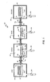
- the system 20 is adapted for depositing an electrical insulator, such as silicon oxide or silicon nitride over a plurality of substrates which are transported on a continuous basis through a plurality of processing chambers including an insulator deposition chamber.
- the system 20 generally includes a load chamber 22, a scrub chamber 24, an insulator or oxide deposition chamber 26, and an unload chamber 28.
- the load chamber 22 is adapted for storing a plurality of substrates 30 upon which the insulator is to be deposited.
- the scrub chamber 24 is adapted for cleaning the surface of the substrates upon which the insulator is to be deposited.
- the insulator deposition chamber 26 is adapted for depositing an electrical insulator, such as silicon oxide, over the substrate surface cleaned in the scrub chamber 24.
- the unload chamber 28 is adapted for receiving the substrates 30 after the electrical insulator has been deposited thereon. If it is not necessary to clean the substrates, the scrub chamber 24 could be an idle chamber wherein no processing is performed to the substrates.
- the chambers 22, 24, 26, and 28 are coupled together in a series arrangement by a plurality of coupling means which include a gas gate 32 which couples the load chamber 22 to the scrub chamber 24, a gas gate 34 which couples the scrub chamber 24 to the insulator deposition chamber 26, and a gas gate 36 which couples the insulator deposition chamber 26 to the unload chamber 28.
- Each of the gas gates 32, 34, and 36 is dimensioned to permit the substrates 30 to pass therethrough as they are transported from one chamber to the next in succession.
- the gas gates 32, 34, and 36 are also dimensioned for conducting gas flow therethrough to provide effective isolation between the chambers of the system.
- each of the chambers 22, 24, 26, and 28 include conveyor means in the form of endless belt conveyors 38, 40, 42, and 44 respectively.
- the conveyors are dimensioned with respect to the dimensions of the substrates 30 and the length of the gas gates 32, 34, and 36 so that before a conveyor releases a substrate it is transporting, the next conveyor is able to grip and support the substrate being transported.
- each endless conveyor includes a pair of belts which are spaced apart so as to contact only opposing side margins of the substrate to enable essentially the entire surface area of the substrate to be exposed for processing.
- the transport means of the system 20 is particularly suited for transporting substrates which are formed from a rigid material such a glass.
- flexible substrates can also be transported if they are mounted in a suitable rigid carrier which provides the support for the substrates at their peripheral margins.
- the belts of the endless conveyors will contact opposing side margins of the carriers.
- the scrub chamber 24 and insulator deposition chamber 26 each include means for forming a glow discharge plasma from a process gas or gases.
- the scrub chamber 24 includes a cathode assembly 46 and a gas inlet 48.
- the insulator deposition chamber 26 includes a cathode assembly 50 and a gas inlet 52.
- the cathode assemblies 46 and 50 are coupled to a source of RF energy (not shown) such as an RF transmitter having an output frequency of 13.58 megahertz, for example.
- the scrub chamber 24 cleans the bottom surface of the substrates 30 by utilizing a glow discharge plasma formed from an appropriate gas, such as argon gas, which is fed to the cathode assembly 46 through the gas inlet 48.
- the insulator deposition chamber 26 deposits an electrical insulator, such as silicon oxide, onto the surface of the substrate 30 which has been cleaned in the scrub chamber 24.
- the insulator is deposited by a glow discharge plasma formed from process gases including, for example, silane (SiH4) and nitrous oxide (N2O) which are fed to the cathode assembly 50 through the gas inlet 52.
- the system 20 includes pressure control means including an absolute pressure control pump 54, 56, 58, and 60 associated with each of the chambers 22, 24, 26, and 28 respectively.
- the absolute pressure control pumps maintain a pressure within the chambers at about 1 Torr to enable the establishment of the glow discharge plasmas within the scrub chamber 24 and the insulator deposition chamber 26.
- the absolute pressure control pump 58 maintains a pressure within the insulator deposition chamber 26 which is slightly lower than the pressures maintained within the scrub chamber 24 and the unload chamber 28 by the absolute pressure control pumps 56 and 60 respectively.
- This maintains a unidirectional gas flow from the scrub chamber 24 and the unload chamber 28 into the insulator deposition chamber 26 as indicated by the arrows 62 and 64.
- the unidirectional gas flow into the insulator deposition chamber 26 serves to isolate the oxide forming constituent elements within the chamber 26 from the interior of the scrub chamber 24 and the unload chamber 28.
- the oxygen required to form the silicon oxide insulator within the deposition chamber 26 can cause contamination within the other chambers.
- Unidirectional gas flow into the insulator deposition chamber 26 as indicated by the arrows 62 and 64 form a barrier to diffusion of the oxygen constituents within the chamber 26 to provide the necessary isolation.
- an inert gas is swept through the gas gates 32, 34, and 36.
- gas conduits 66, 68, and 70 are provided.
- the inert gas can be, for example, argon gas.
- the gas conduits 68 and 70 cause the inert gas to be swept through the gas gates 34 and 36 in the direction of the unidirectional gas flow as indicated by the arrows 62 and 64.
- the conduits are provided on opposite sides of the gas gates so that the inert gas is swept across both the top and bottom surfaces of the substrates as they pass through these gas gates.
- the conduits 66 cause the inert gas to be swept through the gas gate 32 from the scrub chamber 24 to the load chamber 22 as indicated by the arrow 72.
- the load chamber 22 and unload chamber 28 are detachable from the system at the flanges 74 and 76.
- a valve 78 can be closed to enable the load chamber 22 to be disconnected from the scrub chamber 24 without necessitating exposing the scrub chamber 24 to ambient pressure.
- a similar load chamber having substrates stored therein can then be connected to the scrub chamber 24 and then pumped down to the appropriate pressure to enable the valve 78 to once again be opened and to initiate a new run of substrates through the system.
- valve 80 can be closed to facilitate the removal of the unload chamber 28 from the insulator deposition chamber 26 and an empty unload chamber to be connected to the insulator deposition chamber 26.
- the valve 80 can once again be opened to initiate the deposition process. This can be accomplished without necessitating the interruption of the glow discharge plasma within the insulator deposition chamber 26.
- a load chamber 22 which is fully loaded with substrates 30 is connected to the scrub chamber 24. Similar technicallyly, an empty unload chamber 28 is connected to the insulator deposition chamber 26.
- the valves 78 and 80 are open and each of the chambers 22, 24, 26, and 28 is pumped down by the pumps 54, 56, 58, and 60 respectively to an appropriate partial vacuum pressure.
- the following parameters and process steps could be utilized, for example, while depositing silicon oxide in the insulator deposition chamber 26.
- the load chamber can be pumped down to a pressure of about .95 Torr, the scrub chamber can be pumped down to a pressure of about 1.00 Torr, the insulator deposition chamber 26 can be pumped down to a pressure of about .95 Torr, and the unload chamber 28 can be pumped down to a pressure of about 1.00 Torr.
- the scrub chamber 24 and insulator deposition chamber 26 are then caused to initiate their RF glow discharge plasmas.
- the gas inlet 48 of the cathode assembly 46 pro vides argon gas at a flow rate of 500 SCCM
- substrate heaters within the interior of the chamber are energized for heating the substrates to a temperature of about 300°C
- RF power is applied to the cathode assembly at a power of about .1 watt per square centimeter of the substrate area.
- the insulator deposition chamber 26 receives at its gas inlet 52 of the cathode assembly 50 a mixture of 5% silane gas with 95% helium gas at a flow rate of 300 SCCM, nitrous oxide gas at a flow rate of 600 SCCM, and argon gas at a flow rate of 300 SCCM.
- Substrate heaters (not shown) within the insulator deposition chamber 26 are energized to heat the substrate to about 350°C and RF power of about .1 watt per square centimeter of substrate area is applied to the cathode assembly 50.
- the pressure differential between the deposition chamber and the adjoining chambers is adjusted to provide a flow rate through the gas gates corresponding to the degree of isolation desired between the chambers.
- the gas conduits 66, 68, and 70 are provided with argon gas at a flow rate corresponding to the desired flow rate through the gas gates.
- the sweep gas flow rate from the gas conduits is 200 SCCM
- the ratio of the concentration of the elemental constituents within the insulator deposition chamber 26 to the concentration of those elements within the scrub chamber 24 and unload chamber 28 immediately adjacent thereto will be on the order of 102.
- the sweep gas flow rate is 800 SCCM, for example, the above noted concentration ratio will be 106.
- a concentration ratio of 105 can be obtained at a sweep gas flow rate of 650 SCCM.
- the degree of isolation desired will largely depend upon the particular application.
- the required degree of isolation can be less than the required degreee of isolation wherein a semiconductor is also deposited, such as in a system of the type shown in Fig. 7.
- a concentration ratio of at least 102 can be entirely satisfactory whereas, in an application of the type shown in Fig. 7 to be described subsequently, a concentration ratio of 105 can be required.
- the degree of isolation between the insulator deposition chamber and the immediately adjacent preceding and succeeding chambers is dependent upon the sweep gas flow rate, the length of the gas gates, the cross-sectional area of the gas gates, the pressure within the gas gates, and the diffusion coefficient which is the measure of how fast one gas moves through another gas at a certain pressure and temperature.
- the sweep gas flow rate, the pressure within the gas gates, and the gas gate dimensions are all interdependent.
- the best way of relating these parameters to the degree of isolation expected is through a gas gate constant G which takes all of these parameters into account.
- the gas gate constant G can be expressed as below.
- the conveyor 38 is energized to commence the one-by-one feeding of the substrates 30 through the gas gate 32 and into the scrub chamber 24.
- the substrates 30 are fed through the chambers from the load chamber 22 to the unload chamber 28 in succession.
- the load and unload chambers are disconnected from the system after the valves 78 and 80 are closed to facilitate the connection of new load and unload chambers to the system.
- the valves 78 and 80 are once again opened and the process is reinitiated.
- the deposition parameters within chamber 26 can be, for example, a substrate temperature of 200°C, a pressure of about .400 Torr, and a process of .03 watts per square centimeter.
- Ammonia gas (NH3) at a flow rate of 300 SCCM and silane (SiH4) at a flow rate of 50 SCCM can be fed to the chamber 26.
- the adjacent chambers can be maintained at a pressure of about .050 Torr above the pressure within chamber 26, or about .450 Torr.
- the sweep gas flow rates previously mentioned can also be used.
- the system 20 of Fig. 1 provides for the deposition of an insulator over the substrates in a continuous process.
- the deposition environment within the insulator deposition chamber 26 need not be interrupted to assure the deposition of a high quality, defect free, insulator over the substrates.
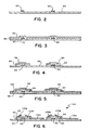
- Figs. 2 through 6 illustrate an intermediate subassembly for a liquid crystal display at various stages of its manufacture which can be made utilizing the system and method of the present invention as shown in Fig. 7. More specifically, the system and method of the present invention can be utilized to form a plurality of layers of various materials over a substrate wherein the plurality of layers include at least an electrically insulating layer and an intrinsic amorphous silicon alloy layer as shown in Fig. 3.
- Fig. 2 it illustrates a substrate 90 formed from an electrical insulator such as glass, having a plurality of electrodes 92 formed thereon.
- the electrodes 92 which will eventually become the gate electrodes for a corresponding plurality of thin film field effect transistors, can be formed from metal, such as chromium, and can be deposited and patterned in a conventional manner.
- the substrate 90 with the electrodes 92 thereon is then processed in accordance with the system and method of the present invention.
- a layer 94 of electrically insulating material such as silicon oxide (SiO x )
- a layer 96 of an intrinsic amorphous silicon alloy are formed over the substrate as shown in Fig. 3.
- Other layers could also be formed such as a layer of doped n-type amorphous silicon alloy.
- the layers 94 and 96 can be deposited in one continuous process wherein the substrate 90 is transported through a plurality of processing chambers in succession.
- the chambers form a closed system wherein a partial vacuum is maintained in each chamber to preclude exposure of the substrate 90 to the external environment between depositions and gas flow is maintained between the chambers as described subsequently to isolate the insulator deposition chamber from the rest of the system.
- the substrate with the layers 94 and 96 thereon are removed from the system and the layers are patterned to form the structure illustrated in Fig. 4.
- the layers 94 and 96 can be patterned by a conventional photolithography process wherein the top most layer 96 is coated with a photoresist. The photoresist is then exposed through a mask and then developed. After the developing step, the layers 94 and 96 are exposed to a suitable etchant to form isolated islands of the layers 94 and 96 as illustrated in Fig. 4.
- a layer 100 of transparent conductive material is next deposited over the structure of Fig. 4 as shown in Fig. 5.
- the layer 100 of transparent conductive material can be formed from indium tin oxide, for example.
- the layer 100 of transparent conductive material is patterned to form drain and source electrodes for each field effect transistor, and a pixel electrode for each pixel.
- each field effect transistor 102 in cludes a gate electrode 92, a gate insulator 94, an intrinsic amorphous silicon alloy 96, a drain electrode 100a, a source electrode 100b, and a pixel electrode 100c coupled to the source electrode 100b.
- an intermediate subassembly 104 is formed which can be used in the manufacture of a liquid crystal display.
- Fig. 7 it illustrates a continuous process system 110 embodying the present invention which can be utilized in the process of making the intermediate subassembly 104 of Fig. 6. More specifically, the system 110 is arranged for producing the partially completed intermediate subassembly as illustrated in Fig. 3. To that end, the system 110 includes means for depositing the electrical insulator layer 94 and the intrinsic amorphous silicon alloy layer 96 over the substrate 90.
- the system 110 includes a load chamber 112, a substrate cleaning chamber 114, an insulator deposition chamber 116, and an unload chamber 118. Each of these chambers performs the same functions as the corresponding chambers previously described with respect to the system 20 of Fig. 1.
- the system 110 includes an intrinsic semiconductor deposition chamber 120.
- the intrinsic semiconductor deposition chamber 120 is arranged for depositing over the insulator deposited onto the substrates within chamber 116 an intrinsic amorphous silicon alloy.
- the system 110 further includes a plurality of gas gates 124, 126, 128, and 130 for coupling the chambers together in a series arrangement.
- the gas gates provide the same function as the gas gates 32, 34, and 36 previously described with respect to the system 20 of Fig. 1.
- Associated with the gas gates are a plurality of sweep gas feed means 134, 136, 138, and 140 which feed an inert sweep gas, such as argon gas, in the direction of the gas flow through the gas gates, on opposite sides of the substrates as they pass therethrough.
- an inert sweep gas such as argon gas
- each of the chambers 112, 114, 116, 120, and 118 includes an endless belt conveyor 146, 148, 150, 152, and 154.
- each such conveyor can include two endless belt conveyors which are spaced apart and substantially parallel to one another for contacting opposing peripheral side margins of the substrates.
- the system 110 further includes cathode assemblies 160, 162, and 164 within the chambers 114, 116, and 120 respectively.
- the cathode assemblies are disposed between the pair of corresponding endless conveyor belts within the chambers 114, 116, and 120 so that they do not interfere with the transportation of the substrates through the chambers.
- the cathode assemblies are also positioned with respect to the substrate surfaces for forming a plasma closely adjacent to the substrate surfaces.
- the cathode assemblies include gas inlets 168, 170, and 172. The gas mixtures received by the cathode assemblies through the gas inlets will be described subsequently.
- the cathode assemblies 160, 162, and 164 are coupled to a source of RF energy (not shown) in a manner well known in the art.
- the RF energy sources are not shown in Fig. 7 so as to not unduly complicate the figure.
- the RF sources can be, for example, RF transmitters having an output frequency of 13.58 megahertz for example.
- the system is a closed system wherein each of the chambers 112, 114, 116, 120, and 118 is pumped down to a partial vacuum pressure.
- each of the chambers is associated with an absolute pressure control pump 176, 178, 180, 182, and 184 which comprise pressure control means for the system 110.
- the system includes a valve 188 associated with the substrate cleaning chamber 114 and valve 190 associated with the intrinsic semiconductor deposition chamber 120.
- the valves 188 and 190 when closed, permit the removal of the load chamber 112 and the unload chamber 118 from the system without losing the vacuum within or contaminating the rest of the system.
- cathode assembly 162 of the insulator deposition chamber 116 is shown in greater detail in Fig. 8.
- One of the conveyor belts is partially shown in Fig. 8 along with a substrate 90 so as to make it easier to understand the operation of the cathode assembly 160.
- the cathode assembly 162 includes the gas inlet 170 through which process gates for the cathode assembly are received and a cathode 192 which is adapted for connection to an RF energy source (not shown).
- the cathode assembly 162 further includes a wall 194 which defines along with a gas conduit 196 a gas mixing chamber 198.
- On the side of the conduit 196 opposite the wall 194 is another wall 199 which serves to direct the unused process gases into the conduit 196 to thereafter be pumped from the system by the pump 180 shown in Fig. 7.
- the process gas flow around the cathode 192 is indicated by the arrows 200.
- An opening 202 within the conduit 196 permits the interior of the chamber 116 to be pumped down to a suitable partial vacuum pressure by the pump by virtue of the spacing between the wall of the chamber 116 and the walls 194 and 199 of the cathode assembly 162.
- the gas gate 126 includes substantially planar side walls 204 and 206, and a pair of generally arcuate side walls 208 and 210 which define a generally rectangular opening 212.
- the walls 206, 208, and 210 include guide projections 214, 216, 218, and 220.
- the guides serve to support and guide the substrate 90 as it passes through the rectangular opening 212.
- the guides 218 and 220 preferably contact the substrate 90 along its side margins outside of the substrate portion to be deposited on and are of particular importance because they separate the substrate 90 from the bottom wall 206 of the gas gate 126 to permit the sweep gas to flow along the bottom side of the substrate 90.
- the rectangular opening 212 and the guides are dimensioned to permit the substrate 90 to pass through the gas gate 126 in a guided manner.
- the inner dimensions of the rectangular opening 212 as an example, can be 16 inches wide, 10 inches long, and 1/4 inch high. Of importance are the length and height dimension of the rectangular opening 212.
- the isolation concentration ratios provided by the unidirectional gas flow described with respect to the exemplary operation of the Fig. 1 system relates to a gas gate having these inner dimensions.
- Fig. 10 illustrates in greater detail one of the gas gates, for example, gas gate 128 in association with the sweep gas feed means 138.
- the sweep gas feed means 138 comprises a pair of conduits 141 which extend along the entire width of the gas gate 128 transverses to the direction of the unidirectional gas flow.
- the conduits 141 communicate with the gas gate through inlet slits 143 which in turn extend along the entire length of the conduits 141.
- the sweep gas is caused to be fed by the sweep gas feed means 138 across the entire surface area of the substrate along the major opposing surfaces thereof as the substrate is transported through the gas gate 128.
- Figs. 11A and 11B they illustrate alternate ways in which the load chamber 112 and unload chamber 118 can be connected and disconnected from the system 110.
- the gas gate thereshown is the gas gate 124 extending between the load chamber 112 and the scrub chamber 114.
- the gas gate 124 includes two portions 222 and 224 with portion 222 being carried by the load chamber 112 and the portion 224 being carried by the scrub chamber 114.
- Each of the portions 222 and 224 includes a flange 226 and 228 respectively.
- the flanges 226 and 228 preferably extend around the entire periphery of the portions 222 and 224.
- a sealing o-ring 230 is provided between the flanges when the portions 222 and 224 are brought together.
- Figs. 11A and 11B illustrate two different alternatives for fixing the flanges together.
- the first alternative in Fig. 11A includes a plurality of bolts, one such bolt 232 being shown, extending through aligned apertures of the flanges and a nut 234 threadingly engaging the bolt 232.
- the other alternative in Fig. 11B includes a u-shaped member 236 which is hingedly coupled to the flange 226 at a hinge 238.
- a threaded member 240 having a knob shaped member 242 at one end and an engagement member 244 at the other end.
- the member 240 is threaded intermediate its ends and mates with a threaded bore within the u-shaped member such that the u-shaped member 236 can be swung to the position illustrated and the knob 242 turned so that the engagement member 244 securely engages the flange 238. With the member 240 tightened, the flanges will be securely held together. Of course, a plurality of such u-shaped members 236 are required. When it is desired to separate the portions 222 and 224, the knob 242 is turned in the opposite direction to loosen the member 240 and disengage the engagement member 244 from the flange 228. The u-shaped member 236 can then be swung out of the way about the hinge 238 to permit the portions 222 and 224 to be separated.
- Fig. 12 is an end view of the load chamber 112 illustrating the major component parts therein.
- the load chamber includes a pair of conveyors 250 and 252 which carry a plurality of stops 254 and 256 respectively. Supported on opposing stops and extending across the chamber are a plurality of substrates 90 to be processed.
- the chamber 112 also includes an endless conveyor with a pair of belts 146 and 148. When the system 110 is in operation, the conveyor belts 250 and 252 lower the stops 254 and 256 in unison such that one of the substrates 90 is placed upon the conveyor belts 146 and 148.
- the conveyors 250 and 252 can be moved continuosly at a slow rate such that the next substrate is placed onto the conveyor belts 146 and 148 immediately after the preceding substrate has passed from the load chamber 112 through the gas gate 124 into the scrub chamber 114 or the belts 240 and 252 can be moved incrementally.
- the pumps 176, 178, 180, 182, and 184 establish partial vacuums within each of the chambers.
- the pumps can establish pressures of about .95 Torr in load chamber 112, about 1.00 Torr in scrub chamber 114, about .95 Torr in the insulator deposition chamber 116, about 1.00 Torr in the intrinsic semiconductor deposition chamber 120, and about .95 Torr in the unload chamber 118.
- These pressures assure unidirectional flow of gas from the scrub chamber 114 and the intrinsic semiconductor deposition chamber 120 into the insulator deposition chamber 116 through the gas gates 126 and 128.
- the inert sweep gas is also caused to be swept through the gas gates 126 and 128 in the direction of the unidirectional gas flow.
- the pressure differentials and the sweep gas flow assure that the insulator deposition chamber 116 is effectively isolated from the other chambers of the system to assure that no deleterious amounts of the oxygen deposition constituents within the insulator deposition chamber 116 diffuse into the chambers adjacent the chamber 116.
- the system is operated such that argon gas is delivered to the gas inlet 168, a 5% mixture of silane with helium is delivered to the cathode inlet 170 at a flow rate of 300 SCCM with nitrous oxide at a flow rate of 600 SCCM, and silane gas is delivered to the cathode gas inlet 172 at a flow rate of 100 SCCM with helium gas at a flow rate of 500 SCCM.
- Each of the cathode assemblies 160, 162, and 164 can be provided with RF power of about .1 watt per square centimeter of substrate area.
- Substrate heaters within the chambers are energized for heating the substrate within the scrub chamber 114 to 300°C, the insulator deposition chamber 116 to 350°C, and the intrinsic semiconductor deposition chamber 120 to 250°C.
- the sweep gas can be provided to the gas gates at a flow rate of 650 SCCM to obtain an isolation concentration ratio of 105, or 800 SCCM to obtain an isolation concentration ratio of 106 as previously referred to.
- the substrates 90 having the gate electrodes 92 formed thereon are provided to the load chamber 112.
- Each of the chambers is pumped down to its appropriate pressure and the glow discharge environments are initiated in each of the chambers having a cathode assembly as previously described.
- the substrates are then placed one at a time onto the conveyor 146 and transported from the load chamber 112 into the scrub chamber 114 and then serially in successivesion through the remaining chambers to the unload chamber 118. In this manner, a plurality of substrates can be processed in the closed environment of the system 110 without being exposed to ambient conditions.
- FIG. 13 it illustrates another system 260 embodying the present invention.
- the system 260 comprises a first chamber 262 and a second chamber 264.
- Chamber 262 comprises a load/unload chamber for storing both unprocessed and processed substrates.
- Chamber 264 comprises an insulator deposition chamber for depositing an insulator such as silicon oxide (S i O x ) over the substrates.
- Chamber 264 is essentially identical to the insulator deposition chambers previously described. It includes a cathode assembly 266 for forming a glow discharge plasma from process gases fed from a gas inlet 268.
- the chamber 264 further includes an endless conveyor 270. Unlike the conveyors previously described, the conveyor 270 is arranged for both receiving the unprocessed substrates from the chamber 262 and for transporting the substrates, after being processed, back to the chamber 262.
- the load/unload chamber 262 includes an endless conveyor 272.
- the conveyor 272 is arranged for transporting the unprocessed substrates 274a disposed above the conveyor to the insulator deposition chamber 264.
- the conveyor is further arranged to receive the processed substrates from the chamber 264 so that the process substrates 274b can be stored below the conveyor 272.
- the conveyors 270 and 272 can be energized to operate in a reverse direction for transporting the processed substrate back to chamber 262. Thereafter, the substrate can be held in a temporary stationary position until the belts of conveyor 272 have been moved laterally by a sufficient distance so as to be clear of the side margins of the substrate.
- the processed substrate can then be lowered to a position below the conveyor for storage.
- the chamber 262 communicates with chamber 264 through a coupling means or gas gate 276.
- the gas gate 276 is dimensioned as previously described to permit the substrates to pass therethrough and to conduct unidirectional gas flow from the chamber 262 to the chamber 264 to provide adequate isolation between the chambers.
- the system includes absolute pressure control pumps 278 and 280.
- the pumps 278 and 280 maintain the internal pressure of chamber 264 below the internal pressure of chamber 262.
- sweep gas feed means 282 of the type previously described, provides a flow of an inert sweep gas, such as argon, through the gas gate in the direction of the unidirectional gas flow.
- a valve 284 is associated with the chamber 264 in the gas gate 276.
- the valve 284 permits the chamber 262 to be separated from chamber 264 after all of the sub strates have been processed and to permit another load/unload chamber having unprocessed substrates therein to be connected to the chamber 264 without requiring interruption of the partial vacuum within the chamber 264.
- the system 260 can be operated by using the same exemplary parameters described with respect to the operation of the systems of Figs. 1 and 7.
- the pressure within chamber 264 can be maintained at about .95 Torr
- the pressure within chamber 262 can be maintained at about 1.00 Torr
- the sweep gas feed rate can be 200 SCCM.
- the oxide deposition including the process gas mixtures and flow rates and the substrate parameter temperature can be the same as described with respect to the oxide deposition chamber 116 of Fig. 7.
- the present invention provides a new and improved system and method for depositing an electrical insulator over a substrate.
- the present invention provides such a system and method which is a continuous process wherein the deposition processes need not be interrupted, and wherein sufficient isolation is provided between the chambers so that contamination of other layers, such as the intrinsic or doped semiconductor layers, does not result.
- the system and method of the present invention also lends itself to mass production of substrates, and particularly to the making of an intermediate subassembly for a liquid crystal dis play or to other circuit arrays of the type incorporating active or passive circuit devices which require a layer of an electrical insulator.
Landscapes
- Chemical & Material Sciences (AREA)
- General Chemical & Material Sciences (AREA)
- Chemical Kinetics & Catalysis (AREA)
- Engineering & Computer Science (AREA)
- Materials Engineering (AREA)
- Mechanical Engineering (AREA)
- Metallurgy (AREA)
- Organic Chemistry (AREA)
- Liquid Crystal (AREA)
- Chemical Vapour Deposition (AREA)
Applications Claiming Priority (2)
| Application Number | Priority Date | Filing Date | Title |
|---|---|---|---|
| US76030585A | 1985-07-29 | 1985-07-29 | |
| US760305 | 1985-07-29 |
Publications (3)
| Publication Number | Publication Date |
|---|---|
| EP0210578A2 true EP0210578A2 (fr) | 1987-02-04 |
| EP0210578A3 EP0210578A3 (en) | 1989-01-18 |
| EP0210578B1 EP0210578B1 (fr) | 1992-05-20 |
Family
ID=25058701
Family Applications (1)
| Application Number | Title | Priority Date | Filing Date |
|---|---|---|---|
| EP86110049A Expired - Lifetime EP0210578B1 (fr) | 1985-07-29 | 1986-07-22 | Appareil et procédé de dépôt en continu d'isolateurs électriques |
Country Status (5)
| Country | Link |
|---|---|
| EP (1) | EP0210578B1 (fr) |
| JP (1) | JPS6230882A (fr) |
| KR (1) | KR870001755A (fr) |
| CA (1) | CA1289512C (fr) |
| DE (1) | DE3685380D1 (fr) |
Cited By (6)
| Publication number | Priority date | Publication date | Assignee | Title |
|---|---|---|---|---|
| EP0430079A3 (en) * | 1989-11-24 | 1992-03-18 | Nihon Shinku Gijutsu Kabushiki Kaisha | Chemical vapor deposition apparatus of in-line type |
| WO2000003422A3 (fr) * | 1998-07-13 | 2000-08-03 | Applied Komatsu Technology Inc | Regulation de flux de gaz dans un systeme de traitement de substrat |
| WO2010089460A1 (fr) * | 2009-02-09 | 2010-08-12 | Beneq Oy | Dispositif de porte, ligne de production, et procédé |
| CN101736306B (zh) * | 2008-11-12 | 2011-11-30 | 北京世纪辉光科技发展有限公司 | 等离子表面冶金金属线材的生产方法及装置 |
| DE102010022277A1 (de) * | 2010-05-31 | 2011-12-01 | Fraunhofer-Gesellschaft zur Förderung der angewandten Forschung e.V. | Vorrichtung und Verfahren zur Reaktivgastrennung in in-line-Beschichtungsanlagen |
| WO2023116961A1 (fr) * | 2021-12-22 | 2023-06-29 | Rainer Cremer | Système en ligne de revêtement de substrats individuels ou de groupes de substrats et procédé de revêtement de substrats individuels ou de groupes de substrats dans un système de revêtement en ligne |
Families Citing this family (3)
| Publication number | Priority date | Publication date | Assignee | Title |
|---|---|---|---|---|
| JP2712796B2 (ja) * | 1990-09-12 | 1998-02-16 | カシオ計算機株式会社 | 薄膜トランジスタの製造方法 |
| JPH06177102A (ja) * | 1990-09-17 | 1994-06-24 | Nippon Telegr & Teleph Corp <Ntt> | 化合物半導体表面の清浄化方法および装置 |
| KR100365423B1 (ko) * | 1995-12-30 | 2003-03-06 | 주식회사 하이닉스반도체 | 반도체소자제조를위한연속공정진행시스템 |
Family Cites Families (5)
| Publication number | Priority date | Publication date | Assignee | Title |
|---|---|---|---|---|
| US4410558A (en) * | 1980-05-19 | 1983-10-18 | Energy Conversion Devices, Inc. | Continuous amorphous solar cell production system |
| JPS5747711A (en) * | 1980-08-08 | 1982-03-18 | Fujitsu Ltd | Chemical plasma growing method in vapor phase |
| US4438723A (en) * | 1981-09-28 | 1984-03-27 | Energy Conversion Devices, Inc. | Multiple chamber deposition and isolation system and method |
| JPS58169980A (ja) * | 1982-03-19 | 1983-10-06 | Matsushita Electric Ind Co Ltd | 光起電力素子の製造方法 |
| US4450786A (en) * | 1982-08-13 | 1984-05-29 | Energy Conversion Devices, Inc. | Grooved gas gate |
-
1986
- 1986-07-22 EP EP86110049A patent/EP0210578B1/fr not_active Expired - Lifetime
- 1986-07-22 CA CA000514424A patent/CA1289512C/fr not_active Expired - Fee Related
- 1986-07-22 DE DE8686110049T patent/DE3685380D1/de not_active Expired - Fee Related
- 1986-07-29 JP JP61178589A patent/JPS6230882A/ja active Pending
- 1986-07-29 KR KR1019860006203A patent/KR870001755A/ko not_active Ceased
Cited By (8)
| Publication number | Priority date | Publication date | Assignee | Title |
|---|---|---|---|---|
| EP0430079A3 (en) * | 1989-11-24 | 1992-03-18 | Nihon Shinku Gijutsu Kabushiki Kaisha | Chemical vapor deposition apparatus of in-line type |
| WO2000003422A3 (fr) * | 1998-07-13 | 2000-08-03 | Applied Komatsu Technology Inc | Regulation de flux de gaz dans un systeme de traitement de substrat |
| US6286230B1 (en) | 1998-07-13 | 2001-09-11 | Applied Komatsu Technology, Inc. | Method of controlling gas flow in a substrate processing system |
| CN101736306B (zh) * | 2008-11-12 | 2011-11-30 | 北京世纪辉光科技发展有限公司 | 等离子表面冶金金属线材的生产方法及装置 |
| WO2010089460A1 (fr) * | 2009-02-09 | 2010-08-12 | Beneq Oy | Dispositif de porte, ligne de production, et procédé |
| CN102308023A (zh) * | 2009-02-09 | 2012-01-04 | Beneq有限公司 | 闸装置、生产线和方法 |
| DE102010022277A1 (de) * | 2010-05-31 | 2011-12-01 | Fraunhofer-Gesellschaft zur Förderung der angewandten Forschung e.V. | Vorrichtung und Verfahren zur Reaktivgastrennung in in-line-Beschichtungsanlagen |
| WO2023116961A1 (fr) * | 2021-12-22 | 2023-06-29 | Rainer Cremer | Système en ligne de revêtement de substrats individuels ou de groupes de substrats et procédé de revêtement de substrats individuels ou de groupes de substrats dans un système de revêtement en ligne |
Also Published As
| Publication number | Publication date |
|---|---|
| JPS6230882A (ja) | 1987-02-09 |
| EP0210578A3 (en) | 1989-01-18 |
| CA1289512C (fr) | 1991-09-24 |
| DE3685380D1 (de) | 1992-06-25 |
| EP0210578B1 (fr) | 1992-05-20 |
| KR870001755A (ko) | 1987-03-17 |
Similar Documents
| Publication | Publication Date | Title |
|---|---|---|
| US4889609A (en) | Continuous dry etching system | |
| US6204197B1 (en) | Semiconductor device, manufacturing method, and system | |
| CA2134241C (fr) | Procede et appareil servant a fabriquer des dispositifs photovoltaiques, et produit resultant | |
| US4763602A (en) | Thin film deposition apparatus including a vacuum transport mechanism | |
| KR910003169B1 (ko) | 반도체 장치 제조 방법 및 장치 | |
| US7011866B1 (en) | Method and apparatus for film deposition | |
| US5589233A (en) | Single chamber CVD process for thin film transistors | |
| CN102598240B (zh) | 垂直整合的处理腔室 | |
| US6444277B1 (en) | Method for depositing amorphous silicon thin films onto large area glass substrates by chemical vapor deposition at high deposition rates | |
| KR100777956B1 (ko) | 플라스마 cvd법 및 장치 | |
| US8865259B2 (en) | Method and system for inline chemical vapor deposition | |
| EP0210578A2 (fr) | Appareil et procédé de dépôt en continu d'isolateurs électriques | |
| US4988642A (en) | Semiconductor device, manufacturing method, and system | |
| KR920003309B1 (ko) | 반도체층 증착장치 | |
| JPH0370367B2 (fr) | ||
| EP0227839A1 (fr) | Procede de formage d'un film mince | |
| JPH09106952A (ja) | 基板上に半導体膜を形成するための装置および方法 | |
| JP2977686B2 (ja) | 光起電力装置の製造方法及びその製造装置 | |
| JPH08260149A (ja) | 減圧表面処理装置及び太陽電池製作装置 | |
| JP3554314B2 (ja) | 堆積膜形成方法 | |
| JPH0831420B2 (ja) | 被膜作製装置 | |
| JP3069682B2 (ja) | 反応室のクリーニング方法 | |
| JP3049203B2 (ja) | 半導体薄膜の形成装置 | |
| JPH08241867A (ja) | プラズマ処理装置およびプラズマ処理方法 | |
| JPH0812848B2 (ja) | 半導体装置製造方法 |
Legal Events
| Date | Code | Title | Description |
|---|---|---|---|
| PUAI | Public reference made under article 153(3) epc to a published international application that has entered the european phase |
Free format text: ORIGINAL CODE: 0009012 |
|
| AK | Designated contracting states |
Kind code of ref document: A2 Designated state(s): DE FR GB IT NL SE |
|
| PUAL | Search report despatched |
Free format text: ORIGINAL CODE: 0009013 |
|
| AK | Designated contracting states |
Kind code of ref document: A3 Designated state(s): DE FR GB IT NL SE |
|
| 17P | Request for examination filed |
Effective date: 19890321 |
|
| 17Q | First examination report despatched |
Effective date: 19900810 |
|
| GRAA | (expected) grant |
Free format text: ORIGINAL CODE: 0009210 |
|
| AK | Designated contracting states |
Kind code of ref document: B1 Designated state(s): DE FR GB IT NL SE |
|
| PG25 | Lapsed in a contracting state [announced via postgrant information from national office to epo] |
Ref country code: IT Free format text: LAPSE BECAUSE OF FAILURE TO SUBMIT A TRANSLATION OF THE DESCRIPTION OR TO PAY THE FEE WITHIN THE PRESCRIBED TIME-LIMIT;WARNING: LAPSES OF ITALIAN PATENTS WITH EFFECTIVE DATE BEFORE 2007 MAY HAVE OCCURRED AT ANY TIME BEFORE 2007. THE CORRECT EFFECTIVE DATE MAY BE DIFFERENT FROM THE ONE RECORDED. Effective date: 19920520 |
|
| REF | Corresponds to: |
Ref document number: 3685380 Country of ref document: DE Date of ref document: 19920625 |
|
| PGFP | Annual fee paid to national office [announced via postgrant information from national office to epo] |
Ref country code: GB Payment date: 19920709 Year of fee payment: 7 |
|
| ET | Fr: translation filed | ||
| PGFP | Annual fee paid to national office [announced via postgrant information from national office to epo] |
Ref country code: FR Payment date: 19920717 Year of fee payment: 7 |
|
| PG25 | Lapsed in a contracting state [announced via postgrant information from national office to epo] |
Ref country code: SE Effective date: 19920723 |
|
| PGFP | Annual fee paid to national office [announced via postgrant information from national office to epo] |
Ref country code: DE Payment date: 19920731 Year of fee payment: 7 |
|
| PG25 | Lapsed in a contracting state [announced via postgrant information from national office to epo] |
Ref country code: NL Effective date: 19930201 |
|
| NLV4 | Nl: lapsed or anulled due to non-payment of the annual fee | ||
| PLBE | No opposition filed within time limit |
Free format text: ORIGINAL CODE: 0009261 |
|
| STAA | Information on the status of an ep patent application or granted ep patent |
Free format text: STATUS: NO OPPOSITION FILED WITHIN TIME LIMIT |
|
| 26N | No opposition filed | ||
| PG25 | Lapsed in a contracting state [announced via postgrant information from national office to epo] |
Ref country code: GB Effective date: 19930722 |
|
| GBPC | Gb: european patent ceased through non-payment of renewal fee |
Effective date: 19930722 |
|
| PG25 | Lapsed in a contracting state [announced via postgrant information from national office to epo] |
Ref country code: FR Effective date: 19940331 |
|
| PG25 | Lapsed in a contracting state [announced via postgrant information from national office to epo] |
Ref country code: DE Effective date: 19940401 |
|
| REG | Reference to a national code |
Ref country code: FR Ref legal event code: ST |
|
| EUG | Se: european patent has lapsed |
Ref document number: 86110049.3 Effective date: 19930204 |