EP0210643A1 - Dispositif pour traiter des matériaux ferromagnétiques à impulsions magnétiques - Google Patents
Dispositif pour traiter des matériaux ferromagnétiques à impulsions magnétiques Download PDFInfo
- Publication number
- EP0210643A1 EP0210643A1 EP86110437A EP86110437A EP0210643A1 EP 0210643 A1 EP0210643 A1 EP 0210643A1 EP 86110437 A EP86110437 A EP 86110437A EP 86110437 A EP86110437 A EP 86110437A EP 0210643 A1 EP0210643 A1 EP 0210643A1
- Authority
- EP
- European Patent Office
- Prior art keywords
- control
- input
- output
- block
- feed
- Prior art date
- Legal status (The legal status is an assumption and is not a legal conclusion. Google has not performed a legal analysis and makes no representation as to the accuracy of the status listed.)
- Granted
Links
- 230000005291 magnetic effect Effects 0.000 title claims abstract description 16
- 239000003302 ferromagnetic material Substances 0.000 title claims abstract description 6
- 238000004804 winding Methods 0.000 claims abstract description 18
- 239000003990 capacitor Substances 0.000 claims description 25
- 230000006698 induction Effects 0.000 abstract description 2
- 239000000463 material Substances 0.000 description 7
- 229910000831 Steel Inorganic materials 0.000 description 1
- NINIDFKCEFEMDL-UHFFFAOYSA-N Sulfur Chemical compound [S] NINIDFKCEFEMDL-UHFFFAOYSA-N 0.000 description 1
- 238000001816 cooling Methods 0.000 description 1
- 230000005347 demagnetization Effects 0.000 description 1
- 238000011161 development Methods 0.000 description 1
- 230000018109 developmental process Effects 0.000 description 1
- 238000010586 diagram Methods 0.000 description 1
- 230000008030 elimination Effects 0.000 description 1
- 238000003379 elimination reaction Methods 0.000 description 1
- 238000005265 energy consumption Methods 0.000 description 1
- 230000005294 ferromagnetic effect Effects 0.000 description 1
- 238000011835 investigation Methods 0.000 description 1
- 230000005415 magnetization Effects 0.000 description 1
- 238000004519 manufacturing process Methods 0.000 description 1
- 238000011089 mechanical engineering Methods 0.000 description 1
- 230000003071 parasitic effect Effects 0.000 description 1
- 238000004904 shortening Methods 0.000 description 1
- 238000001228 spectrum Methods 0.000 description 1
- 239000010959 steel Substances 0.000 description 1
- 229910052717 sulfur Inorganic materials 0.000 description 1
- 239000011593 sulfur Substances 0.000 description 1
- 230000001360 synchronised effect Effects 0.000 description 1
- XLYOFNOQVPJJNP-UHFFFAOYSA-N water Substances O XLYOFNOQVPJJNP-UHFFFAOYSA-N 0.000 description 1
Images
Classifications
-
- H—ELECTRICITY
- H03—ELECTRONIC CIRCUITRY
- H03K—PULSE TECHNIQUE
- H03K17/00—Electronic switching or gating, i.e. not by contact-making and –breaking
- H03K17/51—Electronic switching or gating, i.e. not by contact-making and –breaking characterised by the components used
- H03K17/56—Electronic switching or gating, i.e. not by contact-making and –breaking characterised by the components used by the use, as active elements, of semiconductor devices
- H03K17/72—Electronic switching or gating, i.e. not by contact-making and –breaking characterised by the components used by the use, as active elements, of semiconductor devices having more than two PN junctions; having more than three electrodes; having more than one electrode connected to the same conductivity region
- H03K17/735—Switching arrangements with several input- or output-terminals, e.g. multiplexers, distributors
-
- H—ELECTRICITY
- H01—ELECTRIC ELEMENTS
- H01F—MAGNETS; INDUCTANCES; TRANSFORMERS; SELECTION OF MATERIALS FOR THEIR MAGNETIC PROPERTIES
- H01F13/00—Apparatus or processes for magnetising or demagnetising
-
- H—ELECTRICITY
- H03—ELECTRONIC CIRCUITRY
- H03K—PULSE TECHNIQUE
- H03K17/00—Electronic switching or gating, i.e. not by contact-making and –breaking
- H03K17/51—Electronic switching or gating, i.e. not by contact-making and –breaking characterised by the components used
- H03K17/56—Electronic switching or gating, i.e. not by contact-making and –breaking characterised by the components used by the use, as active elements, of semiconductor devices
- H03K17/72—Electronic switching or gating, i.e. not by contact-making and –breaking characterised by the components used by the use, as active elements, of semiconductor devices having more than two PN junctions; having more than three electrodes; having more than one electrode connected to the same conductivity region
- H03K17/73—Electronic switching or gating, i.e. not by contact-making and –breaking characterised by the components used by the use, as active elements, of semiconductor devices having more than two PN junctions; having more than three electrodes; having more than one electrode connected to the same conductivity region for DC voltages or currents
- H03K17/731—Electronic switching or gating, i.e. not by contact-making and –breaking characterised by the components used by the use, as active elements, of semiconductor devices having more than two PN junctions; having more than three electrodes; having more than one electrode connected to the same conductivity region for DC voltages or currents with inductive load
Definitions
- the invention relates to a device for magnetic pulse treatment of ferromagnetic materials, which is used in mechanical engineering to change the physical-mechanical properties.
- a device for magnetic pulse treatment of ferromagnetic materials which has a force inductor and a control system.
- the force inductor has an inductor coil, two supply inputs, two control inputs and a control output, and consists of two identical circuits, each of which contains a series circuit consisting of the winding of the inductor coil and a capacitor, in parallel with which a thyristor is connected.
- the common point of the anode of the thyristor with the capacitor is connected to the corresponding feed input, and the common point of the cathode of the thyristor with the corresponding winding is grounded.
- the control electrode of each thyristor is connected to the corresponding control input of the inductor Start data provider is with the. Control output connected.
- the control system has two feed outlets, each of which is connected to the corresponding feed inlet of the force inductor; two control outputs, each of which is connected to the corresponding control input of the inductor; a control input connected to the control output of the inductor; a block for controlling the thyristors, the outputs of which are connected to the corresponding control output; a control block, the input of which is connected to the control output and the output of which is connected to the input of the block for controlling the thyristors.
- a second output of the control block is connected to a control input of a feed block, which is designed as an adjustable, stabilized current-flow converter, the outputs of which are connected to the corresponding feed output.
- the AC input of the supply block is connected to an AC supply input of the control system, which input is connected via a second supply block to the supply input of the block for controlling the thyristor.
- a disadvantage of the device is the insufficiently effective treatment of the materials, caused by the insufficiently good characteristics of the magnetic field, which consist in limited maximum magnetic induction, working frequency and homogeneity. These disadvantages arise due to the presence of two windings in the inductor coil, which limit the range of dimensions of the material to be treated, and due to the presence of a parasitic magnetic field during the charging of the capacitors over the winding which is not working at the moment.
- the invention has for its object to provide a device for magnetic pulse processing of ferromagnetic tools, in which the effectiveness of the treatment of the material is increased by improving the characteristics of the magnetic field.
- An advantage of the device according to the invention is the increased effectiveness of the treatment of the material, as a result of which its physico-mechanical properties, e.g. its wear resistance, can be improved.
- Another advantage is the ability to optimize and automate the parameters of the field of influence, the ability to control more than one force inductor and the ability to connect the device to flexible automated manufacturing systems.
- the energy consumption is reduced by the diode connected in parallel with each capacitor.
- the invention is explained with reference to the embodiment shown in the drawing.
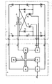
- the drawing shows the circuit diagram of a device according to the invention for the magnetic pulse treatment of ferromagnetic materials.
- the device consists of a force inductor 1 and a control arrangement 2.
- the force inductor 1 contains two feed inputs 3 and 4, two control inputs 5 and 6, a control output 7 and two series circuits connected in parallel, each consisting of a first diode 8 and 9, each having a capacitor 10 and 11 and a second diode 12 and 13, respectively.
- the anodes of the first diodes 8, 9 are connected to one feed input 3 and the cathodes of the second diodes 12, 13 to the other feed input 4.
- the winding 14 of an inductor coil and the anode of a thyristor 15 and 16 are connected to the connection points of the first diodes 8, 9 with the capacitors 10, 11, the cathode of which is connected to the other terminal of the capacitor 11, connected to the other thyristor 16, 15. 10 is connected.
- the control electrodes of the thyristors 15, 16 are connected to the control input 5 and 6 of the inductor 1, respectively.
- a feedback data transmitter 17 is connected to the winding 14, the output of which is connected to the control output 7 of the inductor 1.
- the control arrangement 2 has an AC feed input 18, two feed outputs 19, 20, two control outputs 21, 22, a control input 23 and a feed block 24. The input of the feed block 24 is connected to the AC input 18.
- One output of the feed block 24 is connected to a feed output 19 via an adjustable key 25, which is designed as an electronic switch regulator the other output of the feed block 24 is connected directly to the feed output 20.
- a synchronizing block 26 is connected on two sides to the feed block 24.
- the synchronization block 26 is also connected via an interface 27 to the controllable switch 25, to a local control block 28 and to a programmable control and display block 29.
- An output of the local control block 28 is connected to a control block 30 for controlling the thyristors 15, 16, while its control input is connected to the control input 23 of the control arrangement 2.
- the feed outputs 19, 20 of the control arrangement 2 are connected to the corresponding feed input 3 or 4 of the inductor 1.
- the control outputs 21, 22 of the control arrangement 2 are connected to the corresponding control inputs 5 and 6 of the inductor 1, the control output 7 of which is connected to the control input 23 of the control arrangement 2.
- the cathode of which is connected to the connection point between winding 14 and capacitor 10 or 11 and whose anode is connected to the connection point between the corresponding capacitor 10 or 11 is connected to the cathode of the corresponding thyristor 16 or 15.
- the device works as follows: The workpiece 31 to be treated is inserted into the winding 14, with the feed block 24 via the controllable switch. 25 one supply output 19 is supplied with a positive potential relative to the other supply output 20.
- the potentials from the feed outputs 19, 20 of the control arrangement 2 become the anodes of the first diodes 8, 9 via the feed inputs 3, 4 of the force inductor 1 and the cathodes of the second diodes 12, 13 which are turned on.
- control pulses are supplied from the control block 30 to the control electrodes of the thyristors 15, 16 at different times.
- the one capacitor for example capacitor 10
- the current flows through winding 14 in a certain direction.
- the other capacitor 11 discharges and a current flows through the winding 14 in the opposite direction.
- the currents with different directions which are obtained at the two times, generate a magnetic pulse field with two poles, which influences the physico-mechanical properties of the material to be treated.
- the magnetization and demagnetization in the magnetic pulse field was in the range of one minute in experimental investigations.
- This current contributes to the reduction and elimination of the voltage, thereby preventing the corresponding capacitor 10 or 11 from being recharged to a voltage with a polarity that is opposite to the working polarity, namely that caused by its charge.
- the capacitors 10, 11 can be with one pole.
- the steepness of the front of the magnetic pulses is improved, which increases the effectiveness of the treatment and shortens the treatment time.
- the sequence and the time at which the thyristors 15, 16 are switched on is determined by them. In this way, the intensity, the polarity and the frequency of the magnetic pulses acting on the workpiece 31, which are generated by the winding 14, are predetermined.
- the treatment will controlled by the feedback data generator 17 and optimized by the local control block 28 and the programmable control and display block 29. After completion of the treatment, the workpiece 31 is demagnetized.
- the device according to the invention was investigated experimentally by treating screw drills with a diameter of 4.8 mm.
- the cutting conditions after the treatment are: cutting speed 24.13 m / min, 1600 rotations / min, feed step 0.1 mm / rotation, depth of the treatment 15 mm, material: ST 45 arch steel, cooling with 5 percent solution of sulfur oil in the water.
- Drills treated with the device according to the invention are twice as wear-resistant as those treated with the known device.
Landscapes
- Engineering & Computer Science (AREA)
- Power Engineering (AREA)
- Magnetic Treatment Devices (AREA)
- Devices For Checking Fares Or Tickets At Control Points (AREA)
- Manufacturing Of Steel Electrode Plates (AREA)
- Dental Preparations (AREA)
- Securing Of Glass Panes Or The Like (AREA)
- Control Of Electrical Variables (AREA)
- Electrical Discharge Machining, Electrochemical Machining, And Combined Machining (AREA)
- Transducers For Ultrasonic Waves (AREA)
- Video Image Reproduction Devices For Color Tv Systems (AREA)
- Treatments Of Macromolecular Shaped Articles (AREA)
- Manufacturing Cores, Coils, And Magnets (AREA)
- Digital Magnetic Recording (AREA)
- Generation Of Surge Voltage And Current (AREA)
- Adhesives Or Adhesive Processes (AREA)
- Hard Magnetic Materials (AREA)
- Crystals, And After-Treatments Of Crystals (AREA)
Priority Applications (1)
| Application Number | Priority Date | Filing Date | Title |
|---|---|---|---|
| AT86110437T ATE44189T1 (de) | 1985-07-29 | 1986-07-29 | Vorrichtung zur magnetimpulsbehandlung von ferromagnetischen werkstoffen. |
Applications Claiming Priority (2)
| Application Number | Priority Date | Filing Date | Title |
|---|---|---|---|
| BG71263/85 | 1985-07-29 | ||
| BG8571263A BG41281A1 (en) | 1985-07-29 | 1985-07-29 | Device for magneto- impulse treatment of ferromagnetic materials |
Publications (2)
| Publication Number | Publication Date |
|---|---|
| EP0210643A1 true EP0210643A1 (fr) | 1987-02-04 |
| EP0210643B1 EP0210643B1 (fr) | 1989-06-21 |
Family
ID=3915982
Family Applications (1)
| Application Number | Title | Priority Date | Filing Date |
|---|---|---|---|
| EP86110437A Expired EP0210643B1 (fr) | 1985-07-29 | 1986-07-29 | Dispositif pour traiter des matériaux ferromagnétiques à impulsions magnétiques |
Country Status (11)
| Country | Link |
|---|---|
| US (1) | US4754177A (fr) |
| EP (1) | EP0210643B1 (fr) |
| JP (1) | JPS6337807A (fr) |
| AT (1) | ATE44189T1 (fr) |
| AU (1) | AU590595B2 (fr) |
| BG (1) | BG41281A1 (fr) |
| CS (1) | CS271091B1 (fr) |
| DD (1) | DD272398A3 (fr) |
| DE (1) | DE3664074D1 (fr) |
| HU (1) | HU203168B (fr) |
| YU (1) | YU134486A (fr) |
Families Citing this family (3)
| Publication number | Priority date | Publication date | Assignee | Title |
|---|---|---|---|---|
| ES2071562B1 (es) * | 1992-06-15 | 1997-11-01 | Selter S A | Unidad electronica para magnetizar y desmagnetizar aparatos electropermanentes. (procede del modelo utilidad 9201899) |
| US5671522A (en) * | 1996-01-29 | 1997-09-30 | Northrop Grumman Corporation | Method and apparatus for sealing a pressure vessel |
| DE10030566C2 (de) * | 2000-06-21 | 2002-09-12 | Rossendorf Forschzent | Schaltungsanordnung zur Erzeugung positiver und negativer pulsförmiger Magnetfelder |
Citations (3)
| Publication number | Priority date | Publication date | Assignee | Title |
|---|---|---|---|---|
| FR1421455A (fr) * | 1964-10-30 | 1965-12-17 | Cie Generale D Electronique In | Circuit générateur d'impulsions |
| EP0101922A1 (fr) * | 1982-07-27 | 1984-03-07 | Zentralen Maschinostroitelen Institut | Procédé et dispositif pour traiter des matériaux ferro-magnétiques |
| GB2156608A (en) * | 1984-02-16 | 1985-10-09 | Hayashibara Ken | Apparatus for generating alternating magnetic flux |
Family Cites Families (4)
| Publication number | Priority date | Publication date | Assignee | Title |
|---|---|---|---|---|
| US3643112A (en) * | 1970-01-09 | 1972-02-15 | Westinghouse Electric Corp | Thyristor gate pulse generator |
| US4017744A (en) * | 1975-12-22 | 1977-04-12 | Westinghouse Electric Corporation | Digital firing pulse generator for thyristor power converters |
| DE3304851A1 (de) * | 1983-02-12 | 1984-08-16 | Reinhausen Maschf Scheubeck | Schaltanordnung fuer lastumschalter von stufenschaltern fuer stufentransformatoren |
| US4551782A (en) * | 1983-09-09 | 1985-11-05 | Rfl Industries, Inc. | Method and apparatus for degaussing magnetic storage media |
-
1985
- 1985-07-29 BG BG8571263A patent/BG41281A1/xx unknown
-
1986
- 1986-07-22 CS CS865571A patent/CS271091B1/cs unknown
- 1986-07-25 YU YU01344/86A patent/YU134486A/xx unknown
- 1986-07-25 HU HU863099A patent/HU203168B/hu not_active IP Right Cessation
- 1986-07-25 DD DD86292851A patent/DD272398A3/de not_active IP Right Cessation
- 1986-07-29 AU AU60731/86A patent/AU590595B2/en not_active Ceased
- 1986-07-29 US US06/891,471 patent/US4754177A/en not_active Expired - Fee Related
- 1986-07-29 DE DE8686110437T patent/DE3664074D1/de not_active Expired
- 1986-07-29 AT AT86110437T patent/ATE44189T1/de not_active IP Right Cessation
- 1986-07-29 JP JP61176837A patent/JPS6337807A/ja active Pending
- 1986-07-29 EP EP86110437A patent/EP0210643B1/fr not_active Expired
Patent Citations (3)
| Publication number | Priority date | Publication date | Assignee | Title |
|---|---|---|---|---|
| FR1421455A (fr) * | 1964-10-30 | 1965-12-17 | Cie Generale D Electronique In | Circuit générateur d'impulsions |
| EP0101922A1 (fr) * | 1982-07-27 | 1984-03-07 | Zentralen Maschinostroitelen Institut | Procédé et dispositif pour traiter des matériaux ferro-magnétiques |
| GB2156608A (en) * | 1984-02-16 | 1985-10-09 | Hayashibara Ken | Apparatus for generating alternating magnetic flux |
Also Published As
| Publication number | Publication date |
|---|---|
| EP0210643B1 (fr) | 1989-06-21 |
| CS271091B1 (en) | 1990-08-14 |
| BG41281A1 (en) | 1987-05-15 |
| YU134486A (en) | 1988-12-31 |
| ATE44189T1 (de) | 1989-07-15 |
| US4754177A (en) | 1988-06-28 |
| DE3664074D1 (en) | 1989-07-27 |
| AU590595B2 (en) | 1989-11-09 |
| HUT41553A (en) | 1987-04-28 |
| JPS6337807A (ja) | 1988-02-18 |
| DD272398A3 (de) | 1989-10-11 |
| CS557186A1 (en) | 1989-06-13 |
| AU6073186A (en) | 1987-02-05 |
| HU203168B (en) | 1991-05-28 |
Similar Documents
| Publication | Publication Date | Title |
|---|---|---|
| EP0268109B1 (fr) | Générateur d'impulsion pour usinage par étincelles | |
| DE2727858A1 (de) | Elektrische entstaubungsvorrichtung | |
| DE2824326C2 (fr) | ||
| EP0186865B1 (fr) | Dispositif d'interruption de décharges en arc dans une enceinte à décharge dans un gaz | |
| DE69525618T2 (de) | Stromversorgungssystem für elektrische entladungsmaschinen | |
| DE112008003599B4 (de) | Entladungsgerät | |
| DE4029578A1 (de) | Leistungsversorgungseinheit fuer ein elektrisches entladungsbearbeitungsgeraet | |
| EP0210643B1 (fr) | Dispositif pour traiter des matériaux ferromagnétiques à impulsions magnétiques | |
| DE102013109797A1 (de) | Ionisator | |
| DE1128063B (de) | Schaltanordnung fuer Elektro-Erosion mit pulsierendem Gleichstrom | |
| DE69226056T2 (de) | Verfahren und Treiber für Feldeffekt-Leistungsschalter mit einer aufgefrischten, ein stabiles Ein-/Ausschalten sicherstellenden Spannungsversorgung | |
| DE2407017C3 (de) | Verfahren und Vorrrichtung zur Elektroerosionsbearbeitung | |
| DE2448218A1 (de) | Zerhackerschaltung | |
| DE10084876B4 (de) | Funkenerosions-Stromversorgungssystem | |
| DE102009008373B4 (de) | Verfahren zum Kondensator-Entladungssschweißen zur Verbindung metallischer Bauteile und Schweißeinheit zur Durchführung des Verfahrens | |
| DE3131037A1 (de) | Verfahren und vorrichtung zum elektrischen entladungsbearbeiten | |
| EP0101922B1 (fr) | Procédé et dispositif pour traiter des matériaux ferro-magnétiques | |
| DE2163614C3 (de) | Vorrichtung zur induktiven Beheizung von Metallobjekten | |
| DE2305707A1 (de) | Elektroerosionsbearbeitung von werkstuecken | |
| DE1487745A1 (de) | Steuersystem fuer Gleichstrommotoren | |
| DE1588249A1 (de) | Schaltungsanordnung zur Drehzahlregelung eines Gleichstrommotors | |
| DE2707590C2 (de) | Kondensatorschweißmaschine | |
| EP1280276A2 (fr) | Dispositif et méthode pour la commutation de transistors | |
| DE3634874A1 (de) | Vorrichtung zur zertruemmerung von koerpersteinen | |
| DE1054614B (de) | Schaltungsanordnung zur Funkenerosion mit automatischer Regelung des Elektrodenvorschubes |
Legal Events
| Date | Code | Title | Description |
|---|---|---|---|
| PUAI | Public reference made under article 153(3) epc to a published international application that has entered the european phase |
Free format text: ORIGINAL CODE: 0009012 |
|
| AK | Designated contracting states |
Kind code of ref document: A1 Designated state(s): AT CH DE FR GB IT LI SE |
|
| 17P | Request for examination filed |
Effective date: 19870325 |
|
| 17Q | First examination report despatched |
Effective date: 19880802 |
|
| GRAA | (expected) grant |
Free format text: ORIGINAL CODE: 0009210 |
|
| AK | Designated contracting states |
Kind code of ref document: B1 Designated state(s): AT CH DE FR GB IT LI SE |
|
| REF | Corresponds to: |
Ref document number: 44189 Country of ref document: AT Date of ref document: 19890715 Kind code of ref document: T |
|
| REF | Corresponds to: |
Ref document number: 3664074 Country of ref document: DE Date of ref document: 19890727 |
|
| ET | Fr: translation filed | ||
| ITF | It: translation for a ep patent filed | ||
| GBT | Gb: translation of ep patent filed (gb section 77(6)(a)/1977) | ||
| PLBE | No opposition filed within time limit |
Free format text: ORIGINAL CODE: 0009261 |
|
| STAA | Information on the status of an ep patent application or granted ep patent |
Free format text: STATUS: NO OPPOSITION FILED WITHIN TIME LIMIT |
|
| 26N | No opposition filed | ||
| PGFP | Annual fee paid to national office [announced via postgrant information from national office to epo] |
Ref country code: GB Payment date: 19900717 Year of fee payment: 5 |
|
| PGFP | Annual fee paid to national office [announced via postgrant information from national office to epo] |
Ref country code: FR Payment date: 19900720 Year of fee payment: 5 |
|
| PGFP | Annual fee paid to national office [announced via postgrant information from national office to epo] |
Ref country code: SE Payment date: 19900726 Year of fee payment: 5 Ref country code: AT Payment date: 19900726 Year of fee payment: 5 |
|
| ITTA | It: last paid annual fee | ||
| PGFP | Annual fee paid to national office [announced via postgrant information from national office to epo] |
Ref country code: CH Payment date: 19900802 Year of fee payment: 5 |
|
| PGFP | Annual fee paid to national office [announced via postgrant information from national office to epo] |
Ref country code: DE Payment date: 19900928 Year of fee payment: 5 |
|
| PG25 | Lapsed in a contracting state [announced via postgrant information from national office to epo] |
Ref country code: GB Effective date: 19910729 Ref country code: AT Effective date: 19910729 |
|
| PG25 | Lapsed in a contracting state [announced via postgrant information from national office to epo] |
Ref country code: SE Effective date: 19910730 |
|
| PG25 | Lapsed in a contracting state [announced via postgrant information from national office to epo] |
Ref country code: LI Effective date: 19910731 Ref country code: CH Effective date: 19910731 |
|
| GBPC | Gb: european patent ceased through non-payment of renewal fee | ||
| PG25 | Lapsed in a contracting state [announced via postgrant information from national office to epo] |
Ref country code: FR Effective date: 19920331 |
|
| REG | Reference to a national code |
Ref country code: CH Ref legal event code: PL |
|
| PG25 | Lapsed in a contracting state [announced via postgrant information from national office to epo] |
Ref country code: DE Effective date: 19920401 |
|
| REG | Reference to a national code |
Ref country code: FR Ref legal event code: ST |
|
| EUG | Se: european patent has lapsed |
Ref document number: 86110437.0 Effective date: 19920210 |
|
| PG25 | Lapsed in a contracting state [announced via postgrant information from national office to epo] |
Ref country code: IT Free format text: LAPSE BECAUSE OF NON-PAYMENT OF DUE FEES;WARNING: LAPSES OF ITALIAN PATENTS WITH EFFECTIVE DATE BEFORE 2007 MAY HAVE OCCURRED AT ANY TIME BEFORE 2007. THE CORRECT EFFECTIVE DATE MAY BE DIFFERENT FROM THE ONE RECORDED. Effective date: 20050729 |