EP0210841A2 - Farbabbildungsgerät - Google Patents
Farbabbildungsgerät Download PDFInfo
- Publication number
- EP0210841A2 EP0210841A2 EP86305678A EP86305678A EP0210841A2 EP 0210841 A2 EP0210841 A2 EP 0210841A2 EP 86305678 A EP86305678 A EP 86305678A EP 86305678 A EP86305678 A EP 86305678A EP 0210841 A2 EP0210841 A2 EP 0210841A2
- Authority
- EP
- European Patent Office
- Prior art keywords
- color
- image pickup
- stripes
- stripe
- scanning
- Prior art date
- Legal status (The legal status is an assumption and is not a legal conclusion. Google has not performed a legal analysis and makes no representation as to the accuracy of the status listed.)
- Granted
Links
Images


Classifications
-
- H—ELECTRICITY
- H04—ELECTRIC COMMUNICATION TECHNIQUE
- H04N—PICTORIAL COMMUNICATION, e.g. TELEVISION
- H04N23/00—Cameras or camera modules comprising electronic image sensors; Control thereof
- H04N23/10—Cameras or camera modules comprising electronic image sensors; Control thereof for generating image signals from different wavelengths
- H04N23/12—Cameras or camera modules comprising electronic image sensors; Control thereof for generating image signals from different wavelengths with one sensor only
Definitions
- the present invention generally relates to color image pickup devices, and more particularly to a color image pickup device which obtains a color multiplexed signal from a pickup tube provided with a color stripe filter and performs a color demodulation in a single tube color television camera, for example.
- a color multiplexed signal is obtained by performing a scan in a direction perpendicular to the longitudinal direction of stripes of a color stripe filter which comprises a repetition of green (G), cyan (C) and white (W or transparent) stripes.
- the scanning is performed in the direction perpendicular to the longitudinal direction of the stripes of the color stripe filter, the color components obtained via the color stripe filter are multiplexed in the scanning direction. For this reason, the frequency band of the luminance signal becomes limited to a narrow frequency band by the color multiplexed signal (carrier), and there is a problem in that it is impossible to obtain a satisfactory horizontal resolution.
- Another and more specific object of the present invention is to provide a color image pickup device in which color components are multiplexed by a carrier having a relatively low carrier frequency. According to the color image pickup device of the present invention, it is possible to obtain a high signal-to-noise ratio and to obtain a satisfactory color reproducibility. In addition, it is possible to have a wide frequency band for the luminance signal and to obtain a satisfactory horizontal resolution. Furthermore, it is possible to obtain an accurate color multiplexed signal waveform even when a longitudinal direction of stripes of a color stripe filter is not perfectly parallel to a scanning direction.
- Still another object of the present invention is to provide a color image pickup device in which a number of scanning lines required to obtain a certain resolution is reduced compared to a number of scanning lines conventionally required to obtain the certain resolution, and generation of color beat is prevented by eliminating an aliasing distortion introduced by a fundamental wave component of the color stripe filter and sampling and eliminating an aliasing distortion introduced by a higher harmonic component and the sampling.
- a color stripe filter 11 a comprises a repetition of green (G), cyan (C) and white (W or transparent) stripes.
- the color image pickup device performs the scanning in a longitudinal direction of the stripes of the color stripe filter 11a.
- a number of scanning lines L is set to such a number that the color stripe filter 11 a can reproduce the samples.
- the number of scanning lines L for one stripe group consisting of the G, C and W stripes is set to six.
- a fundamental wave component and a second harmonic component are to be reproduced.
- a signal obtained from an image pickup tube 11 which is provided with the color stripe filter 11a a shown in FIG.2 is passed through a preamplifier 12 and is supplied to an analog-to-digital (A/D) converter 13 wherein the signal is converted into a digital signal.
- the output digital signal of the A/D converter 13 is supplied to field memories 14a and 14b.
- a control signal is supplied to the memories 14a and 14b from a switching circuit 15 so as to control write-in and read-out operations of the memories 14a and 14b.
- One period of the stripe groups of the color stripe filter 11 a is set to correspond to one horizontal scanning period of the NTSC system.
- a signal from the A/D converter 13 related to a first stripe group S1 is written into the memory 14a as shown in FIG.3A in a sequence of sampled data at sampling points a11, a12, a13, ..., a21, a22, a23, ..., a31, a32, a33, ... shown in FIG.2.
- the sampled data related to the first stripe group S1 are successively written into the memory 14a in the sequence of the sampled data arranged in the horizontal direction.
- the stored sampled data related to the first stripe group S1 are successively read out from the memory 14a in a sequence of the sampled data at the sampling points a11, a21, a31, a41, a51, a61, a12, a22, a32, a42, a52, a62, a13, a23, a33, a43, a53, a63, ....
- the stored sampled data are read out from the memory 14a in the sequence of the stored sampled data arranged in a direction perpendicular to the write-in direction.
- a signal from the A/D converter 13 related to a second stripe group S2 is written into the memory 14b as shown in FIG.3B in a sequence of sampled data at sampling points a71, a72, a73, ..., a81, a82, a83, ..., a91, a92, a93, ... , similarly as in the case of the write-in to the memory 14a in the first horizontal scanning period.
- a third horizontal scanning period the stored sampled data related to the second stripe group S2 are successively read out from the memory 14b in a sequence of the sampled data at the sampling points a71, a81, a91, ..., a72, a82, a92, ..., a73, a83, a93, ....
- the stored sampled data are read out from the memory 14b in the sequence of the stored sampled data arranged in a direction perpendicular to the write-in direction.
- a signal from the A/D converter 13 related to a third stripe group is newly written into the memory 14a.
- the write-in and read-out operations are alternately performed in the memories 14a and 14b for the signal related to each stripe group, and such operations are repeated.
- the write-in and read-out operations are performed for each stripe group, that is, for each horizontal scanning period.
- the signals read out from the memories 14a and 14b for every one horizontal scanning period of the NTSC system are supplied to a digital-to-analog (D/A) converter 16 wherein the signals are converted into an analog signal.
- D/A digital-to-analog
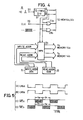
- FIG.4 An embodiment of the switching circuit 15 is shown in FIG.4.
- a horizontal synchronizing signal HD is applied to a terminal 20 and is supplied to a 1/2 frequency divider 21 wherein the signal is frequency-divided by 1/2.
- signals LNSa and LNSb shown in FIGS.5(A) and 5-(B) are obtained from the frequency divider 21.
- a clock signal CLK is applied to a terminal 22 and is supplied to OR gates 23a and 23b which are respectively supplied with the signals LNSa and LNSb.
- write-in and read-out control signals WEa and WEb shown in FIGS.5(C) and 5(D) are obtained from the OR gates 23a and 23b.
- a write-in address generated by a write-in address generator 24 and a read-out address generated by a read-out address generator 25 are supplied to a multiplexer 26.
- This multiplexer 26 is also supplied with the output signals LNSa and LNSb of the frequency divider 21. Hence, the multiplexer 26 alternately produces the write-in address and the read-out address with a period of one horizontal scanning period, in synchronism with the timing of the signal LNSa, for example.
- the output address of the multiplexer 26 is supplied to the memories 14a and 14b.
- the memory 14a performs a write-in operation responsive to the control signal WEa to write data at a write-in address.
- the memory 14a performs a read-out operation responsive to the control signal WEb to read out stored data from a read-out address.
- the memory 14a alternately performs the write-in operation and the read-out operation for every one horizontal scanning period, and such write-in and read-out operations are repeated.
- the memory 14b performs the write-in and read-out operations similarly as in th6 case of the memory 14a, except that the memory 14b performs the read-out operation while the memory 14a performs the write-in operation and performs the write-in operation while the memory 14a performs the read-out operation.
- the signals LNSa and LNSb from the frequency divider 21 are also supplied to data latch circuits (not shown) which are respectively provided at input and output stages of the memories 14a and 14b, so as to control the timings of input and output data of the memories 14a and 14b to regular timings.
- the output signal of the D/A converter 16 comprises the data of each stripe group arranged on the time base as shown in FIG.6.
- This signal shown in FIG.6 is similar to a color multiplexed signal obtained in accordance with the general energy step system.
- the output signal of the D/A converter 16 becomes similar to the color multiplexed signal obtained by multiplexing the color components according to the energy step system, and it is possible to reproduce a fundamental wave component signal and a second harmonic component signal with a high fidelity even when the sampling phase and frequency change.
- the output signal of the D/A converter 16 is supplied to a color demodulating circuit 17 which has a construction similar to a color demodulating circuit used in the case of the energy step system, and is subjected to a color demodulation.
- An output signal of the color demodulating circuit 17 is obtained via an output terminal 18.
- the scanning is performed in the longitudinal direction of the stripes of the color stripe filter 11 a.
- the signal-to-noise ratio is high.
- the image pickup tube can reproduce the color stripes with a high fidelity, and the color reproducibility is satisfactory.
- the scanning is performed in the longitudinal direction of the stripes of the color stripe filter 11a, the color components obtained via the color stripe filter 11a are not multiplexed in the horizontal direction (scanning direction). For this reason, it is possible to obtain the same resolution as in the case of a black-and-white picture, and the frequency band of the luminance signal will not be limited by the color multiplexed signal (carrier).
- the frequency band of the luminance signal can be made wide, and it is possible to obtain a satisfactory horizontal resolution.
- the scanning direction of the image pickup tube 11 and the longitudinal direction of the stripes of the color stripe filter 11 a are perfectly parallel to each other. For this reason, no problems occur.
- the scanning direction that is, the direction of the scanning lines L
- the longitudinal direction of the stripes are not perfectly parallel to each other but are slightly deviated as shown in FIG.7A due to deflection rotation, distortion and the like. As a result, the following problems occur.
- FIG.7A and FIG.7B which will be described later, the inclination of the scanning direction with respect to the longitudinal direction of the stripes is shown exaggeratedly for convenience' sake.
- the modulation degree of the image pickup tube is ' finite (that is, the beam spot is finite)
- it is impossible to discriminate whether the data at a sampling point such as the sampling point a23 which is at a border of the C and W stripes is related to the cyan or white information.
- the scanning direction is slightly deviated from the longitudinal direction of the stripes, the problems described above do not occur just at one position but occur at various positions.
- the memory 14a is designed so that the data are decimated in the horizontal direction and are written into the memory 14a in the sequence of the sampled data at the sampling points a11, a12, a13, a14 across a21, a22, a23, a24, ..., a31, a32, ... with the sampling positions shifted by 1/6 of a sampling period T for each scanning line as shown in FIG.7B. It should be noted that only the main sampling points are shown in FIGS.7A and 7B for convenience' sake.
- the stored sampled data are read out from the memory 14a in the sequence of the sampled data at the sampling points a11, a21, a31, a41, a51, a61, a12, a22, a32, ... , that is, in the sequence of the sampled data arranged in the vertical direction.
- the memory 14b is designed similarly to the memory 14a.
- the present embodiment it is possible to sample all of the green, cyan and white information.
- the color stripe filter 11a comprises 240 stripe groups - (corresponding to one field of the NTSC system).
- the vertical resolution for one stripe group is two television scanning lines
- the vertical resolution as a whole is 480 television scanning lines
- the vertical resolution is the same as that of the conventional image pickup device.
- the color stripe filter should be arranged so that the longitudinal direction of the stripes of the color stripe filter coincides with the vertical direction.
- the write-in to the memories 14a and 14b is performed in a sequence of the data arranged in the vertical direction and the read-out from the memories 14a and 14b is performed in a direction perpendicular to the write-in direction, that is, in the horizontal direction.
- the color multiplexed signal is obtained for each of the stripe groups arranged in the direction approximately perpendicular to the scanning direction. For this reason, the sampled data can be written into and read out from the memories for every one horizontal scanning period of the NTSC system, and it is unnecessary to provide special means for dividing the sampled data read out from the memories into a data group for every one horizontal scanning period. Consequently, the memory capacities of the memories do not need to be extremely large.
- the color multiplexed signal is obtained with the sampling positions shifted in the scanning direction for each scanning line, it is possible to continuously reproduce the color multiplexed signal waveform even when the scanning direction and the longitudinal direction of the stripes are not perfectly parallel to each other.
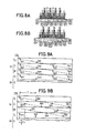
- FIGS.9A and 9B show a portion of the color stripe filter used in the second embodiment for explaining the relationship between the scanning lines and the sampling positions.
- the present embodiment is designed to perform the scanning in a direction inclined by a predetermined angle with respect to the longitudinal direction of the G, C and W stripes of the color stripe filter 11 a.
- FIG.9A and FIG.98 which will be described later, the inclination of the scanning direction with respect to the longitudinal direction of the stripes is shown exaggeratedly for convenience' sake.
- the relative positions of two mutually adjacent sampling points on the scanning line are such that the two mutually adjacent sampling points are deviated in the direction perpendicular to the longitudinal direction of the stripes by 1/2 the repetition pitch of the scanning lines.
- sampling points b12 is arranged in the middle of sampling points b11 and b21 along the direction perpendicular to the longitudinal direction of the stripes (that is, along a direction approximately perpendicular to the scanning direction).
- a sampling point b13 is arranged in the middle of sampling points b12 and b22 along the direction approximately perpendicular to the scanning direction, and other sampling points are arranged with similar relationships.
- the signal obtained from the image pickup tube 11 which is provided with the color stripe filter 11 a shown in FIG.9A is passed through the preamplifier 12 and is supplied to the A/D converter 13 wherein the signal is converted into a digital signal.
- the output digital signal of the AID converter 13 is supplied to the memories. 14a and 14b.
- a control signal is supplied to the memories 14a and 14b from the switching circuit 15 so as to control write-in and read-out operations of the memories 14a and 14b.
- One period of the stripe groups of the color stripe filter 11 a is set to correspond to one horizontal scanning period of the NTSC system.
- a signal from the A/D converter 13 related to the first stripe group S1 is written into the memory 14a as shown in FIG.10A in a sequence of sampled data at sampling points b11, b12, b13, ..., b21, b22, b23, ..., b31, b32, b33, ... shown in FIG.9A.
- the stored sampled data related to the first stripe group Sl are successively read out from the memory 14a in a sequence of the sampled data at the sampling points b11, b12, b21, b22, b31, b32, b12, b13, b22, b23, b32, b33, b13, b14, b23, b24, b33, b34, ....
- the sam-file data at the two mutually adjacent sampling points along the scanning direction and the sampled data at three adjacent sampling points along the direction approximately perpendicular to the scanning direction are taken as a group of six sampled data, and the sampled data at the sampling points which are adjacent to each other along the scanning direction and along the direction approximately perpendicular to the scanning direction are alternately read out from the memory 14a for each of such groups of six sampled data.
- a signal from the A/D converter 13 related to the second stripe group S2 is written into the memory 14b as shown in F1G.10B in a sequence of the sampled data at sampling points b41, b42, b43, ..., b51. b52, b53, ..., b61, b62, b63, ..., similarly as in the case of the write-in to the memory 14a in the first horizontal scanning period;
- a third horizontal scanning period the stored sampled data related to the second stripe group S2 are successively read out from the memory 14b in a sequence of the sampled data at the sampling points b41, b42, b51, b52, b61, b62, .... Furthermore, in this third horizontal scanning period, a signal from the A/D converter 13 related to a third stripe group is newly written into the memory 14a.
- the write-in and read-out operations are alternately performed in the memories 14a and 14b for the signal related to each stripe group, and such operations are repeated.
- the write-in and read-out operations are performed for each stripe group, that is, for each horizontal scanning period.
- the signals read out from the memories 14a and 14b for every one horizontal scanning period of the NTSC system are supplied to the D/A converter 16 wherein the signals are converted into an analog signal.
- the result obtained is equivalent to the case where substantially two scanning lines exist in the direction approximately perpendicular to the scanning direction for each filter stripe (that is, equivalent to the case where substantially six scanning lines exist for each stripe group consisting of the G, C and W stripes) when the sampled data in each of the groups of six sampled data are al-. ternately read out from the memory as described before.
- the output signal of the D/A converter.16 is similar to the color multiplexed signal obtained in accordance with the general energy step system.
- the fundamental wave component and the second harmonic component are to be reproduced:
- the fundamental wave component and the second harmonic component are to be reproduced when there are four or more scanning lines in one stripe group.
- the output signal of the D/A converter 16 comprises the information of the groups of six sampled data for each stripe group arranged on the time base as shown in F)G.11.
- the green information can only be sampled once, at the sampling points b12 and b33, in the second and third groups of six sampled data following the first group of six sampled data.
- the output signal of the D/A converter 16 is similar to the color multiplexed signal obtained by multiplexing the color components according to the energy step system, and it is possible to reproduce the fundamental wave component and the second harmonic component signal with a high fidelity even when the sampling phase and frequency change.
- the memory 14a may be designed so that the data are decimated in the horizontal direction and are written into the memory 14a with the sampling positions shifted by 1/3 the sampling period T for each scanning line as shown in FIG.9B. It should be noted that only the main sampling points are shown in F1GS.9A and 9B for convenience' sake. In this case, the memory 14b may be designed similarly to the memory 14a. In this case, the effects obtained are the same as those obtained by the arrangement shown in FIG.9A.
- each sampling point is in the middle of two sampling points adjacent thereto.
- the sampling phase of a group A consisting of the sampling points b11, b21 and b31 and the sampling phase of a group B consisting of the sampling points b12, b22 and b32 are shifted by 180° with respect to the color stripe filter 11a.
- the aliasing distortions (D and 2 shown in FIG.12 in the group A have polarities opposite to those in the group B. Therefore, when the sampling is performed as in the present embodiment, the aliasing distortions in the group A and the aliasing distortions in the group B will cancel each other, and the color beat will not be generated.
- the interval between two mutually adjacent sampling points on the scanning line along the direction approximately perpendicular to the scanning direction is not limited to 1/2 the repetition pitch of the scanning lines. It is possible to reproduce the fundamental wave component and the second harmonic component even when the interval is set to a value smaller or greater than 1/2 the repetition pitch of the scanning lines.
- the scanning direction is inclined by the predetermined angle with respect to the longitudinal direction of the stripes of the color stripe filter so that the interval between two mutually adjacent sampling points on the scanning line along the direction approximately perpendicular to the scanning direction is within the repetition pitch of the scanning lines
- the number of scanning lines required to obtain a specific resolution is smaller than the number conventionally required to obtain the specific resolution. Consequently, the frequency band of the video signal can be reduced.
- the interval between two mutually adjacent sampling points on the scanning line along the direction approximately perpendicular to the scanning direction is 1/2 the repetition pitch of the scanning lines, it is possible to cancel the aliasing distortions as described before, and the generation of the color beat can be effectively prevented.
Landscapes
- Engineering & Computer Science (AREA)
- Multimedia (AREA)
- Signal Processing (AREA)
- Color Television Image Signal Generators (AREA)
Applications Claiming Priority (4)
| Application Number | Priority Date | Filing Date | Title |
|---|---|---|---|
| JP60166195A JPS6226994A (ja) | 1985-07-27 | 1985-07-27 | カラ−撮像装置 |
| JP166195/85 | 1985-07-27 | ||
| JP166196/85 | 1985-07-27 | ||
| JP60166196A JPS6226995A (ja) | 1985-07-27 | 1985-07-27 | カラ−撮像装置 |
Publications (3)
| Publication Number | Publication Date |
|---|---|
| EP0210841A2 true EP0210841A2 (de) | 1987-02-04 |
| EP0210841A3 EP0210841A3 (en) | 1988-11-09 |
| EP0210841B1 EP0210841B1 (de) | 1991-05-22 |
Family
ID=26490656
Family Applications (1)
| Application Number | Title | Priority Date | Filing Date |
|---|---|---|---|
| EP86305678A Expired EP0210841B1 (de) | 1985-07-27 | 1986-07-24 | Farbabbildungsgerät |
Country Status (3)
| Country | Link |
|---|---|
| US (1) | US4757377A (de) |
| EP (1) | EP0210841B1 (de) |
| DE (2) | DE3679356D1 (de) |
Families Citing this family (1)
| Publication number | Priority date | Publication date | Assignee | Title |
|---|---|---|---|---|
| JP2772579B2 (ja) * | 1990-10-25 | 1998-07-02 | 株式会社リコー | 撮像装置 |
Family Cites Families (15)
| Publication number | Priority date | Publication date | Assignee | Title |
|---|---|---|---|---|
| US2884483A (en) * | 1955-03-09 | 1959-04-28 | Grimson Color Inc | Color image pick up apparatus |
| GB1092881A (en) * | 1963-01-31 | 1967-11-29 | Emi Ltd | Improvements relating to colour television apparatus |
| US3558807A (en) * | 1967-06-10 | 1971-01-26 | Sony Corp | Color video pickup system with means for generating a frequency modulated indexing signal higher in frequency than the video information |
| GB1324271A (en) * | 1969-08-30 | 1973-07-25 | Tokyo Shibaura Electric Co | Colour television image pickup apparatus |
| US3763480A (en) * | 1971-10-12 | 1973-10-02 | Rca Corp | Digital and analog data handling devices |
| CH556626A (de) * | 1971-10-21 | 1974-11-29 | Grundig Emv | Farbfernsehkamera mit einer bildaufnahmeroehre. |
| JPS5143925B2 (de) * | 1971-12-27 | 1976-11-25 | ||
| US3846579A (en) * | 1972-06-03 | 1974-11-05 | Victor Company Of Japan | Color television signal generating apparatus |
| AT326742B (de) * | 1973-01-03 | 1975-12-29 | Eumig | Verfahren zum gewinnen von video-signalen und vorrichtung zur durchfuhrung des verfahrens |
| US4041528A (en) * | 1975-02-20 | 1977-08-09 | Victor Company Of Japan, Limited | Color television signal generating apparatus for use in a single camera tube |
| JPS5935550B2 (ja) * | 1979-03-12 | 1984-08-29 | 日本ビクター株式会社 | カラ−テレビジヨン信号発生装置 |
| US4318123A (en) * | 1980-06-05 | 1982-03-02 | Rca Corporation | Solid-state, color-encoding television camera |
| JPS5934772A (ja) * | 1982-08-20 | 1984-02-25 | Olympus Optical Co Ltd | 画像信号処理装置 |
| JPS5997292A (ja) * | 1982-11-26 | 1984-06-05 | Victor Co Of Japan Ltd | カラ−テレビジヨン撮像装置 |
| US4546380A (en) * | 1983-08-24 | 1985-10-08 | Rca Corporation | Solid-state color-encoding television camera |
-
1986
- 1986-07-23 US US06/889,687 patent/US4757377A/en not_active Expired - Fee Related
- 1986-07-24 EP EP86305678A patent/EP0210841B1/de not_active Expired
- 1986-07-24 DE DE8686305678T patent/DE3679356D1/de not_active Expired - Fee Related
- 1986-07-24 DE DE198686305678T patent/DE210841T1/de active Pending
Also Published As
| Publication number | Publication date |
|---|---|
| US4757377A (en) | 1988-07-12 |
| DE210841T1 (de) | 1987-05-21 |
| EP0210841A3 (en) | 1988-11-09 |
| DE3679356D1 (de) | 1991-06-27 |
| EP0210841B1 (de) | 1991-05-22 |
Similar Documents
| Publication | Publication Date | Title |
|---|---|---|
| US4774581A (en) | Television picture zoom system | |
| CA1129075A (en) | Television picture compressor | |
| GB2090505A (en) | Television receivers | |
| EP0287331B1 (de) | Speichersystem für bemusterte Daten, zum Beispiel für ein Bildvergrösserungssystem in einem Fernsehempfänger | |
| US4039784A (en) | Digital minimum/maximum vector crt display | |
| JPH0125276B2 (de) | ||
| EP0167343B2 (de) | Zeilenfolgeabtastungs-Fernsehempfänger mit adaptischer Speicheradressierung | |
| HK1004048B (en) | Sampled data memory system eg for a television picture magnification system | |
| EP0093143B1 (de) | Verfahren und anordnung zur verzerrungskorrektur in einem bild das elektronisch aufgezeichnet und linienweise aufgebaut ist | |
| EP0210841B1 (de) | Farbabbildungsgerät | |
| US5065230A (en) | Video signal processor for simultaneously reproducing a plurality of video information on a single monitor picture tube | |
| US5083849A (en) | Light signal sampling system | |
| EP0291347B1 (de) | Verfahren und Einrichtung zur Bildverarbeitung | |
| EP0228900B1 (de) | Farbbildaufnahmeeinrichtung | |
| EP0207661B1 (de) | Farbabbildungsgerät | |
| US4829369A (en) | Color television image pickup device with a stripe filter | |
| US4920410A (en) | Drive method for synchronizing scanning and modulation of flat-configuration color CRT | |
| US5124784A (en) | Video signal processing apparatus | |
| US4757375A (en) | Color television image pickup device with a stripe filter parallel to scanning direction | |
| JPH0630324A (ja) | ワイド画面対応撮像装置 | |
| JP2619075B2 (ja) | 映像信号記憶装置 | |
| JPS59110286A (ja) | 欠陥チヤンネルによる映像の改善方法 | |
| JPS6210985A (ja) | カラ−撮像装置 | |
| JPS621389A (ja) | カラ−撮像装置 | |
| JPS62289893A (ja) | 液晶表示装置 |
Legal Events
| Date | Code | Title | Description |
|---|---|---|---|
| PUAI | Public reference made under article 153(3) epc to a published international application that has entered the european phase |
Free format text: ORIGINAL CODE: 0009012 |
|
| AK | Designated contracting states |
Kind code of ref document: A2 Designated state(s): DE FR GB |
|
| EL | Fr: translation of claims filed | ||
| DET | De: translation of patent claims | ||
| 17P | Request for examination filed |
Effective date: 19870731 |
|
| PUAL | Search report despatched |
Free format text: ORIGINAL CODE: 0009013 |
|
| AK | Designated contracting states |
Kind code of ref document: A3 Designated state(s): DE FR GB |
|
| 17Q | First examination report despatched |
Effective date: 19900116 |
|
| GRAA | (expected) grant |
Free format text: ORIGINAL CODE: 0009210 |
|
| AK | Designated contracting states |
Kind code of ref document: B1 Designated state(s): DE FR GB |
|
| REF | Corresponds to: |
Ref document number: 3679356 Country of ref document: DE Date of ref document: 19910627 |
|
| ET | Fr: translation filed | ||
| PLBE | No opposition filed within time limit |
Free format text: ORIGINAL CODE: 0009261 |
|
| STAA | Information on the status of an ep patent application or granted ep patent |
Free format text: STATUS: NO OPPOSITION FILED WITHIN TIME LIMIT |
|
| 26N | No opposition filed | ||
| PGFP | Annual fee paid to national office [announced via postgrant information from national office to epo] |
Ref country code: FR Payment date: 19940711 Year of fee payment: 9 |
|
| PGFP | Annual fee paid to national office [announced via postgrant information from national office to epo] |
Ref country code: GB Payment date: 19940714 Year of fee payment: 9 |
|
| PGFP | Annual fee paid to national office [announced via postgrant information from national office to epo] |
Ref country code: DE Payment date: 19940721 Year of fee payment: 9 |
|
| PG25 | Lapsed in a contracting state [announced via postgrant information from national office to epo] |
Ref country code: GB Effective date: 19950724 |
|
| GBPC | Gb: european patent ceased through non-payment of renewal fee |
Effective date: 19950724 |
|
| PG25 | Lapsed in a contracting state [announced via postgrant information from national office to epo] |
Ref country code: DE Effective date: 19960402 |
|
| PG25 | Lapsed in a contracting state [announced via postgrant information from national office to epo] |
Ref country code: FR Effective date: 19960430 |
|
| REG | Reference to a national code |
Ref country code: FR Ref legal event code: ST |
|
| REG | Reference to a national code |
Ref country code: FR Ref legal event code: ST |
|
| REG | Reference to a national code |
Ref country code: FR Ref legal event code: ST |