EP0210862A2 - Gerät zum Ausgleich von Bewegung in einem von einem von einem Fernsehsignal abgeleiteten Bild - Google Patents
Gerät zum Ausgleich von Bewegung in einem von einem von einem Fernsehsignal abgeleiteten Bild Download PDFInfo
- Publication number
- EP0210862A2 EP0210862A2 EP86305793A EP86305793A EP0210862A2 EP 0210862 A2 EP0210862 A2 EP 0210862A2 EP 86305793 A EP86305793 A EP 86305793A EP 86305793 A EP86305793 A EP 86305793A EP 0210862 A2 EP0210862 A2 EP 0210862A2
- Authority
- EP
- European Patent Office
- Prior art keywords
- field
- memories
- pair
- output
- image
- Prior art date
- Legal status (The legal status is an assumption and is not a legal conclusion. Google has not performed a legal analysis and makes no representation as to the accuracy of the status listed.)
- Granted
Links
Images


Classifications
-
- H—ELECTRICITY
- H04—ELECTRIC COMMUNICATION TECHNIQUE
- H04N—PICTORIAL COMMUNICATION, e.g. TELEVISION
- H04N7/00—Television systems
- H04N7/01—Conversion of standards, e.g. involving analogue television standards or digital television standards processed at pixel level
- H04N7/0135—Conversion of standards, e.g. involving analogue television standards or digital television standards processed at pixel level involving interpolation processes
- H04N7/014—Conversion of standards, e.g. involving analogue television standards or digital television standards processed at pixel level involving interpolation processes involving the use of motion vectors
Definitions
- This invention relates to apparatus for compensating movement in a picture derived from a television signal.
- Such apparatus is particularly, but not exclusively, suitable for use when converting television signals from one television system to another and, more particularly, for use when correcting for movement in a television image in a field number conversion system.
- movement commands are formed by respectively multiplying the derived movement vector by the coefficients of 1/5, 2/5, 3/5, 4/5 and 1.
- the movement vector is typically derived in the form of x samples, y lines, where x and y are integers, and the input image is shifted in response to these scaled movement commands, thereby forming more accurately positioned output images.
- the movement commands in both the horizontal and vertical directions are rounded to the nearest whole number, for example, by counting fractions over one-half as one and discarding anything less than one-half.
- apparatus for correcting movement in a television signal picture image in a vertical direction comprising:
- the invention provides movement correcting apparatus for shifting a television image in which a movement command is formed based upon a movement vector derived from the input image, and an output is then formed that is image shifted in dependence on this movement command.
- a movement command is formed based upon a movement vector derived from the input image, and an output is then formed that is image shifted in dependence on this movement command.
- embodiments of the present invention use an image of the first field of the input image and an image of the second field of the input signal that are derived from the same field and made to exist simultaneously. Using this special movement command permits the image shifting operation to shift the image 0.5 line in the vertical direction, thereby improving the accuracy of the movement correction in the vertical direction.
- Embodiments of the present invention are intended for use in a field number conversion system, such as one that converts an NTSC television signal for display on a PAL television receiver.
- embodiments of the present invention are particularly suitable for the case of converting a high definition television (HDTV) signal of 1125 lines, sixty fields into a PAL signal of 625 lines, fifty fields.
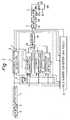
- Figure 1 is a schematic of a system suitable for use in performing such conversion of an HDTV signal for display on a PAL television set.
- a luminance component of a high definition television signal is supplied at an input terminal 1 and fed to an analog-to- digital (A/D) converter 3 through a low-pass filter (LPF) 2.
- A/D analog-to- digital
- LPF low-pass filter
- the digitized luminance signal from the A/D converter 3 is fed to a preprocessing circuit 4 that converts the HDTV signal into a signal having the number of lines suitable for the PAL system, and executes a non-interlacing process, as will be explained below.
- the number of lines in the HDTV signal is converted from 1125 to 625 by use of a digital frequency converting technique, for example.
- video images formed as first and second fields, each consisting of 625 lines are simultaneously formed from a video image that was formed as one field of the high definition television signal. These two field images are identical and, thus, are non-interlaced. Accordingly, although referred to as fields they could also be accurately referred to as frames.
- the first and second fields are substantially identical, there is an offset of 0.5 line in the vertical direction between the respective video images of the first and second fields. Therefore, a digital video signal consisting of only a field field of 625 lines, sixty frames and a digital video signal consisting of only a second field of 625 lines, sixty frames are simultaneously produced as outputs by the preprocessing circuit 4.
- Figure 2A represents a video field showing the scanning lines after the line number conversion has been performed by the preprocessing circuit 4 of Figure 1.
- the circles represent pixels that make up the image
- the solid lines represent the first field and the broken lines represent the second field.
- the data of the first field is shown in Figure 2B and the data of the second field is shown in Figure 2C, and these two fields are simultaneously, respectively supplied on the two output lines from the preprocessing circuit 4.
- a pair of lines such as, for example, the 23rd line of the first field and the 336th line of the second field are simultaneously supplied.
- a pair of lines such as the 24th and 337th lines, a pair of lines such as the 25th and 338th lines, a pair of lines such as the 26th and 339th lines, and so on, are simultaneously supplied.
- the image of the second field ( Figure 2C) is lower by one line than the image of the first field ( Figure 28), although these fields are substantially identical, because they are both taken from the same HDTV field.
- the image of the first field is one line above the image of the second field.
- the movement vector is detected using the video signal of the first field, and the field number converting process is carried out for each of the first and second fields.
- the movement vector is detected at every 1/60 second, so that the detecting accuracy can be improved and the interpolation signal can be easily formed.
- a movement vector detection processing circuit 5 receives the digital video signal of the first field from the preprocessing circuit 4.
- Image shift commands derived from the detected movement vectors are supplied to the field number converters 11 and 21 from the movement vector detection processing circuit 5.
- the movement vector detection processing circuit 5 calculates field difference data, which is the difference between the representative point of the preceding field for every detection region and the pixel of the current field, collects the absolute values of these field difference data, generates the field difference total data, and detects the minimum value of the field difference total data.
- the two output signals of the field number converters 11 and 21 are respectively supplied to a switching circuit 31.
- a control signal which is inverted every 1/50 of a second, is supplied to the switching circuit 31 to cause it to alternate its output between the two input signals. In the interest of brevity and clarity, the control signal for the switching circuit 31 is not shown.
- a digital luminance signal of 625 lines, fifty fields is supplied from the switching circuit 31.
- This digital luminance signal is supplied to a digital-to-analog (D/A) converter 32 and the output signal of the D/A converter 32 is supplied to a PAL colour encoder 34 through a low-pass filter (LPF) 33.
- a red colour difference signal R-Y and blue colour difference signal B-Y which have been subjected to the line number conversion and the field number converting processes just as the luminance signal Y, are also supplied to the PAL colour encoder 34.
- a compound colour television signal of the PAL system is produced at an output terminal 35 of the PAL colour encoder 34.
- a colour television receiver of the PAL system is then connected to the output terminal 35.
- the operation of the first field number converter 11 will now be described. As shown in Figure 1, it comprises a field memory 13, a movement correcting circuit 14, a linear approximating circuit 15, a switching circuit 16, a misprocess detecting circuit 17, and a memory 18.
- the second field number converter 21 is exactly the same as the first field number converter 11.
- Both the digital video signal of the preceding field that is supplied from the field memory 13, and the input digital video signal of the current field that is supplied from the preprocessing circuit 4 are fed to the movement correcting circuit 14, to the linear approximating circuit 15, and to the misprocess detecting circuit 17.
- the data of the preceding field of the second field and the date of the current field are also supplied to the movement correcting circuit 14 from the second field number converting circuit 21.
- Either the output signal of the movement correcting circuit 14 or the output signal of the linear approximating circuit 15 is selected by the switching circuit 16 in response to a detection signal output from the misprocess detecting circuit 17.
- the correction output signal from the switching circuit 16 is thereby selected to be the correction signal that is the more accurate.
- the misprocess detecting circuit 17 is described in more detail below, however, as shown in Figure 1, both the signals of the video image of the preceding field of the first field, which had been field shifted and formed in the movement correcting circuit 14, and the signal of the video image of the current field of the first field, which had been field shifted and formed in the movement correcting circuit 14, are supplied to the misprocess detecting circuit 17. Also supplied to the misprocess detecting circuit 17 are the original video image of the preceding and current fields of the first field before being fed to the movement correcting circuit 14. The selected output of the switching circuit 16 is supplied to the memory 18 that provides time base expansion.
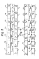
- FIG. 3 An example of the movement correction that is performed by the movement correcting circuit 14 is shown in Figure 3, in which Fl, F2, F3, F4, F5 and F6 denote six continuous images of the first field.
- These images include a moving object which performs uniform motion such that it moves a distance v from left to right at every 1/60 of a second.
- the rate v is actually the movement vector as detected by the movement vector detection processing circuit 5.
- the sum of the amounts of movement from the image Fl to the image F6 equals 5v, therefore, in the case of converting six images, Fl to F6, into five images fl to f5, it is necessary to increase the distance of movement by v/5 at each field.
- the image Fl of the preceding field is not shifted (zero) and the image F2 of the current field which is shifted one full increment (-v) are added, and the resultant added output is divided by two thereby to form the image at the field fl.
- the image f2 is similarly formed from the preceding image F2, which is shifted by v/5 and the current image F3, which is shifted by -4v/5.
- the image f3 is formed from the preceding image F3, which was shifted by 2v/5, and the current image F4, which was shifted by -3v/5.
- the image f4 is formed from the preceding image F4, which was shifted by 3v/5, and the current image F5, which was shifted by -2v/5.
- the image f5 is formed from the preceding image F5, which was shifted by 4v/5, and the current F6, which was shifted by -v/5.
- An image f6 is also formed from the preceding image F6, which was shifted by v, and the current image F11, which is not shifted (zero).
- the resultant image f6 is the same as an image fll of the next field which is formed from the preceding image Fll, which is not shifted (zero), and the current image F12 (not shown), which would be shifted by -v. Therefore, the overlapped or redundant image f6 is discarded. Thereafter, the correcting operations represented in Figure 3 are continously repeated. From the above and the values represented with the shift arrows in Figure 3, it is seen that generally the process is to shift the preceding field by av/5 and to shift the current field by -(5-a)v/5. These shift processes can be executed commonly with the shifting processes which will be needed for the misprocess detection, which will be explained below.
- the image of the preceding field which was shifted by av/5 is essentially the same as the image of the current field which was shifted by -(5-a)v/5, by adding these two images and dividing by two, the signal-to-noise (S/N) ratio due to the random noise in the case of the linear approximation, and the S/N ratio due to the random noise in the case of the movement correction can be equalized.
- S/N signal-to-noise
- the effect is to produce an unfocused or fuzzy image.
- the field number conversion can be completely performed using movement correction as described in relation to Figure 3, however, if in the actual image there is a portion having various kinds of motions, even in one picture plane, or if there is a portion of the image that is still, there will be a problem caused due to the image shift.
- the output of the linear approximating circuit 15 is selected by the switching circuit 16 in place of the output of the movement correcting circuit 14.
- the linear approximating circuit 15 serves as an interpolating circuit for multiplying predetermined weight coefficients with the continuous video images of two fields, respectively, and adding the resultant multiplied outputs.
- An example of correction by the linear approximating circuit 15 is described with reference to Figure 4, in which the images Fl to F6 are six continuous images, which are derived at every 1/60 of a second. These images include both a moving object, which performs uniform motion, and a still object. Note that there is no uniform motion rate, such as v, as there was in the movement correction example explained in Figure 3.
- the images indicated by broken lines denote the images of the current field, which are also present in the shift field (f l , f 2 , ...) but which cannot be seen due to the integration effect of human vision.
- the first converted image of fl is set to correspond to the image at F2, and the image f2 is formed by adding the preceding image F2, which was multiplied with the weight coefficient of 4/5 and the current image, which is F3 multiplied with the weight coefficient of 1/5.
- the image f3 is formed by adding 3/5 F3 and 2/5 F4; the image f4 is formed by adding 2/5 F4 and 3/5 F5; and the image f5 is formed by adding 1/5 F5 and 4/5 F6.
- the misprocess detecting circuit 17 in which the digital video signal of the preceding field Fl is supplied to a first input terminal 41, and the digital video signal of the current field F2 is supplied to a second input terminal 42. Both of these input digital video signals are subtracted for every pixel in a subtractor 43, so that the difference A FL between the signals of both fields is obtained.
- the signal of the field fll of which the image of the preceding field F1 was shifted by, for example, 2v/5 is supplied to a third input terminal 44, and the signal of the next field f12 of which the image of the current field F2 was shifted by, for example, -3v/5 is supplied to a fourth input terminal 45.
- the difference signals ⁇ FL and ⁇ f from the subtractors 43 and 46, respectively, are compared in a comparator 47.
- the image of the field fll, which is the image of the preceding field F1 shifted by 2v/5, and the image of the field f12, which is the image of the current field F2 shifted by -3v/5, in this example are the same with respect to the moving portion, so that the difference image ⁇ f between both images from the subtractor 46 results in an image in which the moving portion is removed.
- the preceding field Fl and the current field F2 which are not shifted are, nevertheless, the same with regard to the still portion and the result (not shown) of the subtractor 43 results in an image in which the still portion is removed.
- the comparator 47 it can be decided that the movement correcting process is correct with respect to the pixel of interest when 4 FL is greater than ⁇ f is detected. On the other hand, it is determined that the movement correction is incorrect with respect to the pixel of interest when ⁇ FL is less than ⁇ f is detected.
- the comparator 47 generates a comparison output which assumes a high "H” level when AFL is greater than ⁇ f and a low “L” level when ⁇ FL is less than A f.
- This comparison output is supplied to a majority logic circuit 48.
- the majority logic circuit 48 decides whether highs or lows are in the majority for every detection region of the movement vector. More specifically, in the comparison of the outputs of a plurality of pixels included in one detection region, when the number of comparison outputs at an "H" level is larger than the number of comparison outputs at an "L” level, an output signal at an "H” level is generated at an output terminal 49.
- This output signal is the control signal fed to the switching circuit 16 that selects the correct signal from movement correcting circuit 14 when the output of the misprocess detecting circuit 17 is at an "H” level or, when the output of the detecting circuit 17 is at an "L” level, selects the corrected signal from the linear approximating circuit 15.
- This movement correction can be effectively accomplished using only one of the signals of the first and second fields.
- the signals of both the first and second fields could be supplied to the movement correcting circuits, thereby improving the accuracy of the movement correction in the vertical direction by a factor of two.
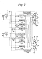
- Figure 7 is a movement correcting circuit according to an embodiment of the present invention, in which the movement correcting circuit for the first field comprises: shift processing memories 51, 52, 53 and 54; shift command change circuits 59 and 60; data selectors 63 and 64; and a decision circuit 67.
- the movement correcting circuit for the second field comprises: shift processing memories 55, 56, 57 and 58; shift command change circuits 61 and 62; data selectors 65 and 66; and a decision circuit 68.
- the shift processing memories 51 to 54 and 55 to 58 operate to shift the image of one field in response to the address control corresponding to the components in the horizontal and vertical directions of the shift command.
- the digital video signal of the current field of the first field, as applied at an input terminal 10, is supplied to the shift processing memories 52 and 54, and the digital video signal of the preceding field of the first field, derived from the field memory 13 also connected to the input terminal 10, is supplied to the shift processing memories 51 and 53.
- the digital video signal of the current field of the second field, as applied to an input terminal 20, is supplied to the shift processing memories 56 and 58, and the digital video signal of the preceding field of the second field, derived from a field memory 23 also connected to the input terminal 20, is supplied to the shift processing memories 55 and 57.
- the shift command relative to the image of the current field is supplied at an input terminal 6, which is one of the outputs of the movement vector detection processing circuit 5 of Figure 1.
- the shift command relative to the image of the preceding field is supplied at an input terminal 7, which is the other of the outputs of the movement vector detection processing circuit 5 of Figure 1.
- These shift commands, as formed by the movement vector detection processing circuit 5, are used to perform the movement correction as shown in Figure 3.
- Figure 3 shows only the movement correcting operation in the horizontal direction, it should be understood that the shift commands are in the form of x samples, y lines, that is, they also provide for shifts in the vertical direction.
- the shift commands regarding the current field are supplied directly to the shift processing memories 52 and 58 and are also supplied through shift command changing circuits 60 and 62 to the shift processing memories 54 and 56, respectively.
- the shift commands with respect to the preceding fields are similarly supplied directly to the shift processing memories 51 and 57, and are also supplied through shift command changing circuits 59 and 61 to the shift processing memories 53 and 55, respectively.
- Both the shift command changing circuits 59 and 60 operate to add "1" to the value of the component y in the vertical direction of the shift command, and both the shift command changing circuits 61 and 62 operate to subtract “1" from the value of the component y in the vertical direction of the shift command. Therefore, the outputs of the shift processing memories 53 and 54 are such that the shift amounts are increased by one line by the shift command change circuits 59 and 60. On the other hand, outputs of the shift processing memories 55 and 56 are such that the shift amounts are decreased by one line by the shift command change circuits 61 and 62.
- this movement correction circuit when the signal of the 24th line of the first field is supplied from the shift processing memories 51 and 52, respectively, the signal of the 25th line of the first field is supplied from the shift processing memories 53 and 54, respectively, and at the same time, the signal of the 337th line that formed the pair with the 24th line is supplied from the shift processing memories 57 and 58, respectively.
- the signal of the 336thl!ne is Supplied from the shift processing memories 55 and 56, respectively.
- Four data selectors 63 to 66 are provided and each of the data selectors 63 to 66 has three input terminals a, b and c and one output terminal d.
- the shifted output signal of the preceding field of the first field is derived at an output terminal 71 connected to the output terminal d of the data selector 63, and the shifted output signal of the current field of the first field is derived at an output terminal 72 connected to the output terminal d of the data selector 64.
- the data selectors 63 and 64 are controlled by respective control signals from the decision circuit 67.
- the signals at the output terminals 71 and 72 are those shown in Figure 1 as being fed to the misprocess detection circuit 17. Whereas, the single output line fed to one input of the switching circuit 16 of Figure 1 is obtained by adding and dividing the two output signals.
- the shift command relative to the current field and the shift command relative to the preceding field from the input terminals 6 and 7, respectively are supplied to the decision circuit 67.
- the shift command regarding the current field is derived by multiplying the detected movement vector v by the coefficients -1, -4/5, -3/5, -2/5, -1/5.
- the shift command relative to the preceding field is obtained by multiplying the detected movement vector v by the coefficients 1/5, 2/5, 3/5, 4/5, 1. Because movement in the vertical direction can only be line to line, the component in the vertical direction of the movement vector v is an integer, a fraction that is an integral times larger than 1/5 occurs in the shift command.
- the decision circuit 67 decides the direction and fraction with regard to each of the shift commands of the current and preceding fields and generates a control signal to cause the appropriate data selector 63 or 64 to select the optimum signal.
- the fractions 2/5 and 3/5 are counted as 0.5, the fraction 1/5 is discarded, and the fraction 4/5 is increased to 1.
- These discarding and increasing processes are executed in the shift processing memories 51 to 54, respectively, whereas the process of converting to the fraction of 0.5 is performed in the decision circuit 67.
- the shift direction is determined to be downward, and when the shift command has a negative sign, the shift direction is determined to be upward.
- the output of the shift processing memory 55 is supplied to the input terminal a for generating the shift output of the preceding field
- the output of the shift processing memory 51 is supplied to the input terminal b
- the output of the shift processing memory 57 is supplied to the input terminal c.
- the output of the shift processing memory 56 is supplied to the input terminal a for generating the shifted output of the current field
- the output of the shift processing memory 52 is supplied to the input terminal b
- the output of the shift processing memory 58 is supplied to the input terminal c.
- each output terminal d of the data selectors 63 and 64 is connected to the input terminal a.
- each output terminal d of the data selectors 63 and 64 is connected to the input terminal c, and when the shift of an integral number of times is decided, each output terminal d of the data selectors 63 and 64 is connected to the input terminal b.
- the data selectors 65 and 66 that are provided relative to the second field operate in a manner similar to data selectors 63 and 64 with respect to the first field. More specifically, the output of the shift processing memory 51 is supplied to the input terminal a of the data selector 65 for generating the shifted output of the preceding field, the output of the shift processing memory 57 is supplied to the input terminal b, and the output of the shift processing memory 53 is supplied to the input terminal c.
- the output of the shift processing memory 52 is supplied to the input terminal a of the data selector 66 for generating the shifted output of the current field, the output of the shift processing memory 58 is supplied to the input terminal b, and the output of the shift processing memory 54 is supplied to the input terminal c.
- Each of the data selectors 65 and 66 selects the signal of the upper or lower line adjacent to the line of the signal to be supplied to the input terminal b in accordance with the control signal from the decision circuit 68, thereby shifting the image in the vertical direction by 0.5 line.
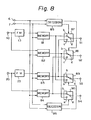
- Figure 8 is another embodiment of a movement correcting circuit according to the present invention, in which the shift processing memories 53 to 56 in the movement correcting circuit of Figure 7 are removed and shift processing memories 81 to 84 respectively corresponding to the shift processing memories 51, 52, 57 and 58, which are inherently necessary to shift the image, are used.
- Outputs of the shift processing memories 81 and 82 are supplied to input terminals b of data selectors 87 and 88, and outputs of the shift processing memories 83 and 84 are supplied to input terminals c of the data selectors 87 and 88.
- the data selectors 87 and 88 are controlled by control signals which are formed by a decision circuit 85.
- the input terminals c of the data selectors 87 and 88 are connected to the output terminals d, so that the shifted output signals of the first field are obtained at output terminals 91 and 92.
- Outputs of the shift processing memories 83 and 84 are supplied to input terminals b of data selectors 89 and 90 relative to the signal of the second field, and outputs of the shift processing memories 81 and 82 are supplied to input terminals of data selectors 89 and 90, respectively.
- the data selectors 89 and 90 are controlled by control signals which are formed by a decision circuit 86.
- the input terminals a and the output terminals d of the data selectors 89 and 90 are connected, respectively.
- the shifted output signals of the second field are derived at output terminals 93 and 94. These outputs are treated in the same fashion as the outputs at the output terminals 73 and 74 of Figure 7.
- the present invention is not limited to the field number converting apparatus in the conversion from the HDTV system to the PAL system, but can be also applied to the conversion from the HDTV system to the SECAM system, band compression transmission, and the like.
- the image shift amount of 0.5 line can be realised, without setting the image shift amount in the vertical direction to an integral line, and counting fractions over 0.5 as one and disregarding the rest, as in the conventional manner. Consequently, the accuracy of the movement correction in the vertical direction can be improved by a factor of 1.5 or two as compared with the conventional accuracy.
- a smooth output image can be formed when processing a moving image which moves at a slow speed.
Landscapes
- Engineering & Computer Science (AREA)
- Multimedia (AREA)
- Signal Processing (AREA)
- Television Systems (AREA)
- Color Television Systems (AREA)
- Picture Signal Circuits (AREA)
- Image Processing (AREA)
- Processing Or Creating Images (AREA)
- Processing Of Color Television Signals (AREA)
Priority Applications (1)
| Application Number | Priority Date | Filing Date | Title |
|---|---|---|---|
| AT86305793T ATE84390T1 (de) | 1985-07-26 | 1986-07-28 | Geraet zum ausgleich von bewegung in einem von einem von einem fernsehsignal abgeleiteten bild. |
Applications Claiming Priority (2)
| Application Number | Priority Date | Filing Date | Title |
|---|---|---|---|
| JP60165075A JPH0746861B2 (ja) | 1985-07-26 | 1985-07-26 | テレビジヨン画像の動き補正装置 |
| JP165075/85 | 1985-07-26 |
Publications (3)
| Publication Number | Publication Date |
|---|---|
| EP0210862A2 true EP0210862A2 (de) | 1987-02-04 |
| EP0210862A3 EP0210862A3 (en) | 1988-11-09 |
| EP0210862B1 EP0210862B1 (de) | 1993-01-07 |
Family
ID=15805391
Family Applications (1)
| Application Number | Title | Priority Date | Filing Date |
|---|---|---|---|
| EP86305793A Expired - Lifetime EP0210862B1 (de) | 1985-07-26 | 1986-07-28 | Gerät zum Ausgleich von Bewegung in einem von einem von einem Fernsehsignal abgeleiteten Bild |
Country Status (6)
| Country | Link |
|---|---|
| US (1) | US4731651A (de) |
| EP (1) | EP0210862B1 (de) |
| JP (1) | JPH0746861B2 (de) |
| AT (1) | ATE84390T1 (de) |
| AU (1) | AU589984B2 (de) |
| DE (1) | DE3687434T2 (de) |
Cited By (3)
| Publication number | Priority date | Publication date | Assignee | Title |
|---|---|---|---|---|
| EP0233720A3 (en) * | 1986-02-19 | 1988-10-05 | Sony Corporation | Television signal - standard converting apparatus |
| GB2205707A (en) * | 1987-06-09 | 1988-12-14 | Sony Corp | Television standards converters |
| WO2001078389A1 (en) * | 2000-04-07 | 2001-10-18 | Snell & Wilcox Limited | Video signal processing |
Families Citing this family (20)
| Publication number | Priority date | Publication date | Assignee | Title |
|---|---|---|---|---|
| US5029001A (en) * | 1986-08-14 | 1991-07-02 | Sony Corporation | NTSC compatible TV signal transmitting system for improving vertical resolution |
| GB8628813D0 (en) * | 1986-12-02 | 1987-01-07 | British Broadcasting Corp | Video display system |
| EP0294961B1 (de) * | 1987-06-09 | 1994-10-12 | Sony Corporation | Auswahl eines Bewegungsvektors in Fernsehbildern |
| KR0125784B1 (ko) * | 1987-10-20 | 1997-12-19 | 이우에 사또시 | 이동 백터 보정 방법 및 장치 |
| US5247353A (en) * | 1989-11-08 | 1993-09-21 | Samsung Co., Ltd. | Motion detection system for high definition television receiver |
| JP2827424B2 (ja) * | 1990-03-31 | 1998-11-25 | ソニー株式会社 | 画振れ補正装置 |
| EP0475499B1 (de) * | 1990-09-03 | 1995-11-22 | Koninklijke Philips Electronics N.V. | Bewegungskompensierte Bildfrequenzumwandlung |
| DE4192565C2 (de) * | 1990-10-23 | 1994-07-07 | Matsushita Electric Industrial Co Ltd | Bildfluktuationserfassungseinrichtung |
| US5243422A (en) * | 1990-11-13 | 1993-09-07 | Hitachi, Ltd. | Field converting method for television signals and device for realizing same |
| JP3116967B2 (ja) * | 1991-07-16 | 2000-12-11 | ソニー株式会社 | 画像処理装置および画像処理方法 |
| DE4126950A1 (de) * | 1991-08-16 | 1993-02-18 | Thomson Brandt Gmbh | Verfahren, coder und decoder zur kompatiblen uebertragung und/oder aufzeichnung von progressiven bildsignalen |
| US5247355A (en) * | 1992-06-11 | 1993-09-21 | Northwest Starscan Limited Partnership | Gridlocked method and system for video motion compensation |
| DE69323572T2 (de) * | 1992-06-11 | 1999-09-16 | Koninklijke Philips Electronics N.V., Eindhoven | Anordnung zum bewegungsausgeglichenen Interpolieren eines Bildsignals |
| GB2272596B (en) * | 1992-11-10 | 1997-06-11 | Sony Broadcast & Communication | Motion compensated video signal processing |
| US6178265B1 (en) * | 1994-09-22 | 2001-01-23 | Intel Corporation | Method and apparatus for motion vector compression |
| EP1104190A4 (de) * | 1999-04-28 | 2006-04-19 | Sony Corp | Gerät und verfahren zur konvertierung von bildsignalen |
| KR100854091B1 (ko) * | 2002-07-13 | 2008-08-25 | 삼성전자주식회사 | 영상신호의 필름 모드 검출장치 및 방법 |
| KR100927143B1 (ko) * | 2002-11-27 | 2009-11-18 | 삼성전자주식회사 | 움직임 검출장치 및 방법 |
| KR20040054032A (ko) * | 2002-12-16 | 2004-06-25 | 삼성전자주식회사 | 영상신호의 포맷 검출장치 및 방법 |
| KR20040055059A (ko) * | 2002-12-20 | 2004-06-26 | 삼성전자주식회사 | 영상포맷의 변환장치 및 방법 |
Citations (3)
| Publication number | Priority date | Publication date | Assignee | Title |
|---|---|---|---|---|
| JPS5728392A (en) | 1980-07-29 | 1982-02-16 | Fujitsu Ltd | Optical semiconductor device |
| JPS5748166A (en) | 1980-09-04 | 1982-03-19 | Toshiba Corp | Character segment device |
| JPS59104866A (ja) | 1982-12-08 | 1984-06-16 | Nippon Hoso Kyokai <Nhk> | テレビジヨン方式変換方法 |
Family Cites Families (10)
| Publication number | Priority date | Publication date | Assignee | Title |
|---|---|---|---|---|
| US4240101A (en) * | 1976-10-14 | 1980-12-16 | Micro Consultants, Limited | Television standards conversion |
| US4272787A (en) * | 1978-09-07 | 1981-06-09 | Micro Consultants Limited | T.V. Picture freeze system |
| DE3072180D1 (de) * | 1979-05-08 | 1990-09-20 | British Broadcasting Corp | Fernseh-wiedergabesystem. |
| GB8328362D0 (en) * | 1983-10-24 | 1983-11-23 | Indep Broadcasting Authority | Movement detector |
| JPS60189388A (ja) * | 1984-03-09 | 1985-09-26 | Fujitsu Ltd | 動き補償符号化装置 |
| US4654876A (en) * | 1984-12-19 | 1987-03-31 | Itek Corporation | Digital image motion correction method |
| US4663665A (en) * | 1985-01-07 | 1987-05-05 | Nippon Hoso Kyokai | TV system conversion apparatus |
| EP0193185B1 (de) * | 1985-02-28 | 1992-05-13 | Mitsubishi Denki Kabushiki Kaisha | Adaptive Zwischenbild-Vektorquantisier-Kodiereinrichtung |
| AU579550B2 (en) * | 1985-06-10 | 1988-11-24 | Nec Corporation | Movement compensation predictive encoder for a moving picture signal with a reduced amount of information |
| AU4852585A (en) * | 1985-10-11 | 1987-04-16 | Iwasaki Engineering Co. Ltd. | Image storage device |
-
1985
- 1985-07-26 JP JP60165075A patent/JPH0746861B2/ja not_active Expired - Lifetime
-
1986
- 1986-07-25 AU AU60570/86A patent/AU589984B2/en not_active Ceased
- 1986-07-25 US US06/889,226 patent/US4731651A/en not_active Expired - Lifetime
- 1986-07-28 AT AT86305793T patent/ATE84390T1/de not_active IP Right Cessation
- 1986-07-28 DE DE8686305793T patent/DE3687434T2/de not_active Expired - Fee Related
- 1986-07-28 EP EP86305793A patent/EP0210862B1/de not_active Expired - Lifetime
Patent Citations (3)
| Publication number | Priority date | Publication date | Assignee | Title |
|---|---|---|---|---|
| JPS5728392A (en) | 1980-07-29 | 1982-02-16 | Fujitsu Ltd | Optical semiconductor device |
| JPS5748166A (en) | 1980-09-04 | 1982-03-19 | Toshiba Corp | Character segment device |
| JPS59104866A (ja) | 1982-12-08 | 1984-06-16 | Nippon Hoso Kyokai <Nhk> | テレビジヨン方式変換方法 |
Cited By (5)
| Publication number | Priority date | Publication date | Assignee | Title |
|---|---|---|---|---|
| EP0233720A3 (en) * | 1986-02-19 | 1988-10-05 | Sony Corporation | Television signal - standard converting apparatus |
| GB2205707A (en) * | 1987-06-09 | 1988-12-14 | Sony Corp | Television standards converters |
| GB2205707B (en) * | 1987-06-09 | 1991-09-04 | Sony Corp | Television standards converters |
| WO2001078389A1 (en) * | 2000-04-07 | 2001-10-18 | Snell & Wilcox Limited | Video signal processing |
| US7009656B2 (en) | 2000-04-07 | 2006-03-07 | Snell & Wilcox Limited | Video signal processing |
Also Published As
| Publication number | Publication date |
|---|---|
| US4731651A (en) | 1988-03-15 |
| EP0210862A3 (en) | 1988-11-09 |
| DE3687434D1 (de) | 1993-02-18 |
| JPS6225591A (ja) | 1987-02-03 |
| ATE84390T1 (de) | 1993-01-15 |
| EP0210862B1 (de) | 1993-01-07 |
| JPH0746861B2 (ja) | 1995-05-17 |
| DE3687434T2 (de) | 1993-05-06 |
| AU6057086A (en) | 1987-01-29 |
| AU589984B2 (en) | 1989-10-26 |
Similar Documents
| Publication | Publication Date | Title |
|---|---|---|
| EP0210862B1 (de) | Gerät zum Ausgleich von Bewegung in einem von einem von einem Fernsehsignal abgeleiteten Bild | |
| AU643565B2 (en) | pideo image processing | |
| US5208667A (en) | Motion compensated video standards converter and method of deriving motion vectors | |
| USRE39278E1 (en) | Method for determining motion compensation | |
| EP0393906B1 (de) | Interpolation eines Videosignals | |
| EP0395265B1 (de) | Bewegungsabhängige Videosignalverarbeitung | |
| KR910003394B1 (ko) | 텔레비젼 수신기에 사용된 비디오 신호의 움직임 검출 회로 | |
| US4663665A (en) | TV system conversion apparatus | |
| US5526053A (en) | Motion compensated video signal processing | |
| US4684985A (en) | Signal converting method and circuit for television receiver | |
| EP0241854B1 (de) | Schaltung zur Verarbeitung eines Videosignals mit Bewegungsadaptation | |
| GB2231752A (en) | Motion dependent video signal processing | |
| US5444493A (en) | Method and apparatus for providing intra-field interpolation of video signals with adaptive weighting based on gradients of temporally adjacent fields | |
| EP1104970B1 (de) | Verfahren und vorrichtung zur umwandlung der zahl von videorahmen von bildsignalen | |
| GB2231746A (en) | Motion dependent video signal processing | |
| GB2231744A (en) | Motion dependent video signal processing | |
| US4791487A (en) | Picture signal conversion device | |
| GB2231747A (en) | Motion dependent video signal processing | |
| USRE39280E1 (en) | Method for determining motion compensation | |
| US5070394A (en) | Image signal processing device | |
| US6233018B1 (en) | Video signal processing | |
| GB2312806A (en) | Motion compensated video signal interpolation | |
| JPH0720238B2 (ja) | 動きベクトル検出回路 | |
| JPH0779459B2 (ja) | 動き補正装置 | |
| JPH0440193A (ja) | Tv方式変換装置の動きベクトル検出方式 |
Legal Events
| Date | Code | Title | Description |
|---|---|---|---|
| PUAI | Public reference made under article 153(3) epc to a published international application that has entered the european phase |
Free format text: ORIGINAL CODE: 0009012 |
|
| AK | Designated contracting states |
Kind code of ref document: A2 Designated state(s): AT DE FR GB NL |
|
| PUAL | Search report despatched |
Free format text: ORIGINAL CODE: 0009013 |
|
| AK | Designated contracting states |
Kind code of ref document: A3 Designated state(s): AT DE FR GB NL |
|
| 17P | Request for examination filed |
Effective date: 19890424 |
|
| 17Q | First examination report despatched |
Effective date: 19910313 |
|
| GRAA | (expected) grant |
Free format text: ORIGINAL CODE: 0009210 |
|
| AK | Designated contracting states |
Kind code of ref document: B1 Designated state(s): AT DE FR GB NL |
|
| REF | Corresponds to: |
Ref document number: 84390 Country of ref document: AT Date of ref document: 19930115 Kind code of ref document: T |
|
| REF | Corresponds to: |
Ref document number: 3687434 Country of ref document: DE Date of ref document: 19930218 |
|
| ET | Fr: translation filed | ||
| PLBE | No opposition filed within time limit |
Free format text: ORIGINAL CODE: 0009261 |
|
| STAA | Information on the status of an ep patent application or granted ep patent |
Free format text: STATUS: NO OPPOSITION FILED WITHIN TIME LIMIT |
|
| 26N | No opposition filed | ||
| REG | Reference to a national code |
Ref country code: GB Ref legal event code: IF02 |
|
| PGFP | Annual fee paid to national office [announced via postgrant information from national office to epo] |
Ref country code: FR Payment date: 20020709 Year of fee payment: 17 |
|
| PGFP | Annual fee paid to national office [announced via postgrant information from national office to epo] |
Ref country code: AT Payment date: 20020711 Year of fee payment: 17 |
|
| PGFP | Annual fee paid to national office [announced via postgrant information from national office to epo] |
Ref country code: GB Payment date: 20020724 Year of fee payment: 17 |
|
| PGFP | Annual fee paid to national office [announced via postgrant information from national office to epo] |
Ref country code: NL Payment date: 20020730 Year of fee payment: 17 |
|
| PGFP | Annual fee paid to national office [announced via postgrant information from national office to epo] |
Ref country code: DE Payment date: 20020731 Year of fee payment: 17 |
|
| PG25 | Lapsed in a contracting state [announced via postgrant information from national office to epo] |
Ref country code: GB Free format text: LAPSE BECAUSE OF NON-PAYMENT OF DUE FEES Effective date: 20030728 Ref country code: AT Free format text: LAPSE BECAUSE OF NON-PAYMENT OF DUE FEES Effective date: 20030728 |
|
| PG25 | Lapsed in a contracting state [announced via postgrant information from national office to epo] |
Ref country code: NL Free format text: LAPSE BECAUSE OF NON-PAYMENT OF DUE FEES Effective date: 20040201 |
|
| PG25 | Lapsed in a contracting state [announced via postgrant information from national office to epo] |
Ref country code: DE Free format text: LAPSE BECAUSE OF NON-PAYMENT OF DUE FEES Effective date: 20040203 |
|
| GBPC | Gb: european patent ceased through non-payment of renewal fee |
Effective date: 20030728 |
|
| PG25 | Lapsed in a contracting state [announced via postgrant information from national office to epo] |
Ref country code: FR Free format text: LAPSE BECAUSE OF NON-PAYMENT OF DUE FEES Effective date: 20040331 |
|
| NLV4 | Nl: lapsed or anulled due to non-payment of the annual fee |
Effective date: 20040201 |
|
| REG | Reference to a national code |
Ref country code: FR Ref legal event code: ST |