EP0211559A1 - Photorécepteur pour électrographie - Google Patents
Photorécepteur pour électrographie Download PDFInfo
- Publication number
- EP0211559A1 EP0211559A1 EP19860305614 EP86305614A EP0211559A1 EP 0211559 A1 EP0211559 A1 EP 0211559A1 EP 19860305614 EP19860305614 EP 19860305614 EP 86305614 A EP86305614 A EP 86305614A EP 0211559 A1 EP0211559 A1 EP 0211559A1
- Authority
- EP
- European Patent Office
- Prior art keywords
- group
- photo
- receptor
- layer
- charge
- Prior art date
- Legal status (The legal status is an assumption and is not a legal conclusion. Google has not performed a legal analysis and makes no representation as to the accuracy of the status listed.)
- Granted
Links
Images
Classifications
-
- G—PHYSICS
- G03—PHOTOGRAPHY; CINEMATOGRAPHY; ANALOGOUS TECHNIQUES USING WAVES OTHER THAN OPTICAL WAVES; ELECTROGRAPHY; HOLOGRAPHY
- G03G—ELECTROGRAPHY; ELECTROPHOTOGRAPHY; MAGNETOGRAPHY
- G03G5/00—Recording-members for original recording by exposure, e.g. to light, to heat or to electrons; Manufacture thereof; Selection of materials therefor
- G03G5/02—Charge-receiving layers
- G03G5/04—Photoconductive layers; Charge-generation layers or charge-transporting layers; Additives therefor; Binders therefor
- G03G5/06—Photoconductive layers; Charge-generation layers or charge-transporting layers; Additives therefor; Binders therefor characterised by the photoconductive material being organic
- G03G5/0622—Heterocyclic compounds
- G03G5/0624—Heterocyclic compounds containing one hetero ring
- G03G5/0635—Heterocyclic compounds containing one hetero ring being six-membered
- G03G5/0638—Heterocyclic compounds containing one hetero ring being six-membered containing two hetero atoms
-
- G—PHYSICS
- G03—PHOTOGRAPHY; CINEMATOGRAPHY; ANALOGOUS TECHNIQUES USING WAVES OTHER THAN OPTICAL WAVES; ELECTROGRAPHY; HOLOGRAPHY
- G03G—ELECTROGRAPHY; ELECTROPHOTOGRAPHY; MAGNETOGRAPHY
- G03G5/00—Recording-members for original recording by exposure, e.g. to light, to heat or to electrons; Manufacture thereof; Selection of materials therefor
- G03G5/02—Charge-receiving layers
- G03G5/04—Photoconductive layers; Charge-generation layers or charge-transporting layers; Additives therefor; Binders therefor
- G03G5/06—Photoconductive layers; Charge-generation layers or charge-transporting layers; Additives therefor; Binders therefor characterised by the photoconductive material being organic
- G03G5/0601—Acyclic or carbocyclic compounds
- G03G5/0612—Acyclic or carbocyclic compounds containing nitrogen
- G03G5/0614—Amines
- G03G5/06142—Amines arylamine
- G03G5/06147—Amines arylamine alkenylarylamine
- G03G5/061473—Amines arylamine alkenylarylamine plural alkenyl groups linked directly to the same aryl group
-
- G—PHYSICS
- G03—PHOTOGRAPHY; CINEMATOGRAPHY; ANALOGOUS TECHNIQUES USING WAVES OTHER THAN OPTICAL WAVES; ELECTROGRAPHY; HOLOGRAPHY
- G03G—ELECTROGRAPHY; ELECTROPHOTOGRAPHY; MAGNETOGRAPHY
- G03G5/00—Recording-members for original recording by exposure, e.g. to light, to heat or to electrons; Manufacture thereof; Selection of materials therefor
- G03G5/02—Charge-receiving layers
- G03G5/04—Photoconductive layers; Charge-generation layers or charge-transporting layers; Additives therefor; Binders therefor
- G03G5/06—Photoconductive layers; Charge-generation layers or charge-transporting layers; Additives therefor; Binders therefor characterised by the photoconductive material being organic
- G03G5/0622—Heterocyclic compounds
- G03G5/0624—Heterocyclic compounds containing one hetero ring
- G03G5/0627—Heterocyclic compounds containing one hetero ring being five-membered
- G03G5/0629—Heterocyclic compounds containing one hetero ring being five-membered containing one hetero atom
-
- G—PHYSICS
- G03—PHOTOGRAPHY; CINEMATOGRAPHY; ANALOGOUS TECHNIQUES USING WAVES OTHER THAN OPTICAL WAVES; ELECTROGRAPHY; HOLOGRAPHY
- G03G—ELECTROGRAPHY; ELECTROPHOTOGRAPHY; MAGNETOGRAPHY
- G03G5/00—Recording-members for original recording by exposure, e.g. to light, to heat or to electrons; Manufacture thereof; Selection of materials therefor
- G03G5/02—Charge-receiving layers
- G03G5/04—Photoconductive layers; Charge-generation layers or charge-transporting layers; Additives therefor; Binders therefor
- G03G5/06—Photoconductive layers; Charge-generation layers or charge-transporting layers; Additives therefor; Binders therefor characterised by the photoconductive material being organic
- G03G5/0622—Heterocyclic compounds
- G03G5/0624—Heterocyclic compounds containing one hetero ring
- G03G5/0635—Heterocyclic compounds containing one hetero ring being six-membered
- G03G5/0637—Heterocyclic compounds containing one hetero ring being six-membered containing one hetero atom
-
- G—PHYSICS
- G03—PHOTOGRAPHY; CINEMATOGRAPHY; ANALOGOUS TECHNIQUES USING WAVES OTHER THAN OPTICAL WAVES; ELECTROGRAPHY; HOLOGRAPHY
- G03G—ELECTROGRAPHY; ELECTROPHOTOGRAPHY; MAGNETOGRAPHY
- G03G5/00—Recording-members for original recording by exposure, e.g. to light, to heat or to electrons; Manufacture thereof; Selection of materials therefor
- G03G5/02—Charge-receiving layers
- G03G5/04—Photoconductive layers; Charge-generation layers or charge-transporting layers; Additives therefor; Binders therefor
- G03G5/06—Photoconductive layers; Charge-generation layers or charge-transporting layers; Additives therefor; Binders therefor characterised by the photoconductive material being organic
- G03G5/0622—Heterocyclic compounds
- G03G5/0624—Heterocyclic compounds containing one hetero ring
- G03G5/0642—Heterocyclic compounds containing one hetero ring being more than six-membered
Definitions
- This invention relates to an electrographic photoreceptor, and more particularly to an electrographic photoreceptor which can improve repetition characteristics without degrading sensitivity.
- the present invention also relates to an electrographic photoreceptor suitable for laser exposure which can improve repetition characteristics without degrading sensitivity and capable of providing good picture images.
- Japanese Patent Laid-Open No. 218447/84 there is disclosed a technology in which the repetition stability of electric potential is improved by adding amine to the composition of a photosensitive layer.
- this technology has the disadvantage of lowering sensitivity.
- Japanese Patent Publication Laid-Open No. 166351/83 and No. 166352/83 there are disclosed technologies in which a polymer of a specified quarternary ammonium salt is used as a binder resin for charge-generating substances.
- this technology requires to control reactivity, compositions or the like, so that it has the disadvantages of lacking production stability, having large fluctuation of characteristics and the lowering sensitivity.
- laser beam printers which utilize the electrophotographic process and form images by using laser light as an optical source have been developed.
- Gas lasers of He-Ne, Ar, etc., or semiconductor lasers as the laser light source.
- an electrographic photoreceptor for usual light source can be utilized, when the wavelength of the laser light source agrees to the spectral sensitivity range of the receptor.
- the moire pattern is the result of the interference of the repetitive reflection light at the air-photosensitive layer interface and the Al-layer surface, and it is considered that when the refelected light from the air-photosensitive layer interface and the reflected light from the Al interface have the same degree of strength, the interference fringes show maximum contrast, and in a half tone picture image, a so-called grain pattern is observed.
- Another object of the present invention is to provide a practically useful electrographic photoreceptor for laser-exposure use, which is stabilized in repetitive characteristics without lowering sensitivity, and satisfies the characteristics required for the electrographic photoreceptor for the laser-exposure use.
- the present invention specifically relates to a photoreceptor for electrography comprising a layer containing a charge-generating substance on an electrically conductive substrate, wherein said photoreceptor comprises a low molecular ammonium salt at a proportion of 0.1 to 15 parts by weight with respect to 100 parts by weight of said charge-generating substance.
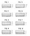
- Figs. 1 through 8 show examples of the cross sectional views of the construction of preferred layers of the electrographic photoreceptors according to the present invention.
- the compounds according to the present invention preferably have a molecular weight of less than 2000, or more preferably less than 1000, and most preferably, less than 750.
- the molecular weight exceeds 2000, the compatibility for the binder lowers, and deposition or the like are likely to occur, which may have disadvantageous effect upon the humidity resistance or the like.
- non-cyclic hydrocarbon group which may have a substituent
- a saturated or unsaturated non-cyclic hydrocarbon group can be cited an alkyl group (especially, alkyl group with carbon number of 1 to 20) and as an unsaturated non-cycle hydrocarbon group, an alkenyl group can be cited (especially, alkenyl group with carbon number 2 to 20), alkinyl group, and alkadienyl group.
- alkyl group especially, alkyl group of carbon number 1 to 20
- alkenyl group especially, alkenyl group of carbon number 2 to 20
- alkyl group in which, alkyl group of carbon number 1 to 20 is most preferable.
- alkyl group as a saturated non-cyclic hydrocarbon group can be cited, for example, methyl group, ethyl group, n-propyl group, iso-propyl group, n-butyl group, iso-butyl group, tertiary butyl group, n-pentyl group, n-hexyl group, n-heptyl group, n-octyl group, 2-ethylhexyl group, dodecyl group, hexadecyl group, octadecyl group and the like.
- alkenyl groups of unsaturated non-cyclic hydrocarbon groups there are, for example, vinyl group, allyl group, 3-methyl-2-butenyl group, isopropenyl group, 2-butynil group, etc.
- alkinyl groups there are ethynil group, butynil group, etc., and as examples of alkadienyl groups, 1, 3-butane dienil group, etc. can be cited.
- substituents for these saturated or unsaturated non-cyclic hydrocarbon groups can be cited halogen atoms as fluorine, chlorine, bromine; cyano groups; hydroxyl groups; acyl groups; alkoxy groups such as methoxy groups, ethoxy groups, etc.; aryl groups such as phenyl groups, etc.; and aryl-oxy groups such as phenoxy groups, etc.
- alkyl groups having a substituent there are, for example, benzyl group, phenethyl group, trithyl group, diphenyl-methyl group, hydroxyethyl group, methoxyethyl group, cyanoethyl group, acethoxyethyl group, acetylethyl group, chloromethyl group, etc.
- alkenyl group having aforementioned substituent there are, for example, styril group, cinnamyl group, etc.
- mono-cyclic hydrocarbon groups for example, mono-cyclic hydrocarbon groups with carbon number 3 to 12
- bridged hydrocarbon groups for example, bridged hydrocarbon groups with carbon number 6 to 18
- condensed multi-ring hydrocarbon groups for example, condensed multi-ring hydrocarbon groups with carbon number 7 to 18
- mono-cyclic hydrocarbon groups can be cited cycloalkyl groups, aromatic groups with mono-cyclic, etc.
- cycloalkyl groups can be cited cyclopentyl group, cyclohexyl group, etc.
- mono-cyclic aromatic group can be cited phenyl group, and the other ones such as cyclododecatrienyl groups, etc. can be cited.
- bridged hydrocarbon groups there are dicylopentadienyl group, norbornyl group, adamantyl group, etc.
- condensed multi-ring hydrocarbon groups there are naphtyl group, anthryl group, phenanthyl group, indenyl group, etc.
- substituents of cyclic hydrocarbon groups can be cited halogen atoms such as fluorine, chlorine, bromine, etc.; alkyl groups such as methyl, ethyl, etc.; cyano group; acyl group; nitro group; hydroxy group; alchoxy groups such as methoxy group, ethoxy group, etc.; and aryloxy groups such as phenoxy group, etc.
- mono-cyclic hydrocarbon groups having these substituent there are, for example, tolyl group, xylyl group, cumenyl group, methoxyphenyl group, mesityl group, etc.
- anions represented by X ⁇ can be sited negative halogen ions such as fluorine, chlorine, bromine, iodine; inorganic acid anions such as tetrafluoroboron ion, hexafluorophosphor ion, carbonic acid ion, sulfuric acid ion, phosphoric acid ion, nitric acid ion, perchloric acid ion, etc.; other inorganic anions such as hydroxy ions, etc.; carbonic acid ions such as acetic acid ion, oxalic acid ion, propionic acid ion, benzoic acid ion, etc.; sulphonic acid ions of such as benzene sulphonic acid; and alchoxy irons such as methoxy iron, ethoxy ion, etc. Above all, halogen ions and the inorganic acid anions are preferable.
- the quadrivalent nitrogen-containing compound is produced by ionizing the trivalent nitrogen of a heterocyclic compound containing trivalent nitrogen, and may contain, other than nitrogen, sulfur, oxygen, selenium, phosphorus, arsenic, silicon, germanium, boron, etc.
- quadrivalent nitrogen-containing cyclic compound those represented by the following general formula (II) or (III) can be mentioned: (wherein, R5, R6 and R9 are independently selected from the group consisting of a hydrogen atom, a non-cyclic hydrocarbon group which may be substituted and a cyclic hydrocarbon group which may be substituted; R7 and R8 are independently groups necessary to complete a substituted or unsubstituted nitrogen-containing heterocyclic group including the quadrivalent nitrogen by being cooperatively connected with each other; R10, R11 and R12 are independently groups to complete a substituted or unsubstituted nitrogen-containing heterocyclic group including the quadrivalent nitrogen being cooperatively connected with each other; and X ⁇ is an anion.)
- X ⁇ denotes a monovalent anion
- X2 ⁇ denotes a divalent anion, respectively
- 2X ⁇ or X2 ⁇ means that either one of 2X ⁇ or X2 ⁇ will attach to the left side structural formula in the same formula.
- two R5 groups combined with different nitrogen atoms may be identical or different. Furthermore, the same notice can be given to the group R6 and also to (E). Further, R9 combined with different nitrogen atoms in (J) may be the same one or a different one. Furthermore, in each of (A) to (K), respectively, as examples of substituents introduced into the mother nucleus can be cited the same ones as described in the above-described general formula 1.
- low molecular weight ammonium salts those represented by the formula (wherein l is an integer of 0 to 3, m is an integer of 1 to 4 provided that l + m is 4, n is an integer of 1 to 20, and X is an anion) are particularly advantageous in the present invention, and more particularly, when l is 2, m is 2, n is an integer of 1 to 8, and X is a halogen atom.
- the electrographic photoreceptor of the present invention is provided, as shown in Figs. 1 to 8, with a charge-generating layer 2 containing charge-generating substance on a conductive substrate 1, but the charge-generating layer containing said charge-generating substance may also contain charge-transporting substance. (Herein strictlyafter, this layer is also referred to as a charge-generating layer.) Also, it may be the one in which the charge-generating layer containing the charge-generating substance and the charge-transporting layer containing the charge-transporting substance are laminated.
- an intermediate layer may be provided between respective layers and a surface protecting layer may also be formed on the uppermost layer.
- the conductive substrate those molded of a metal such as aluminium, brass, stainless steel, etc. in drum-like form or made into a sheet form or a foil, are used. Also, insulating materials of the high polymers such as polyethylene terephthalate, nylon, polyarylate, polyimide, polycarbonate, etc., hardened paper and the like are used by molding in drum-like form or by making them in form of a sheet after they are treated to acquire conductivity.
- conductive treatment there are such ones as the immersion in a conductive substance, lamination of a metal foil (for example, aluminium foil), vapor deposition of a metal (for example, aluminium, indium, tin oxide, yttrium, etc.), conductive finishing method, and the like.
- a metal foil for example, aluminium foil
- vapor deposition of a metal for example, aluminium, indium, tin oxide, yttrium, etc.
- conductive finishing method and the like.
- conductive substrates can be cited films of polyethylene phthalate or the like vapor-depositied with an aluminium, titanium, etc., or an aluminium drum subjected to mirror finishing.
- the electrographic photoreceptor according to the present invention preferably has a subbing layer and as a material suitable for said subbing layer may be metal oxide such as aluminium oxide, indium oxide, titanium oxide, etc.; macromolecular materials such as acrylic resins, methacrylic resins, vinyl chloride resins, vinyl acetate resins, epoxy resins, urethan resins, polyester resins, phenolic resins, alkyd resins, polycarbonate resins, silicone resins, melamine resins, polyvinylformal resins, polyvinylbutyral resins, polyvinyl alcohol resins, vinyl chloride-vinyl acetate maleic acid anhydride copolymer, vinylidene chloride-acrylonitrile copolymer, styrene-butadiene copolymer, etc.; and cellulosic materials such as ethylcellulose, carboxymethyl cellulose, etc. These can be used alone or in combination of two or more kinds.
- the subbing layer is formed by dissolving above-described materials in a suitable solvent, and coating on a conductive substrate to a predetermined film thickness.
- a suitable solvent for dissolving above-described materials in a suitable solvent
- coating in case when the conductive substrate is made drum-like, the immersion method, spray method, extrusion or slide hopper method or the like are preferable, and when the conductive substrate is in sheet-like form, the roll method, extrusion or slide hopper method are preferably adopted.
- the film thickness of a subbing layer formed in such a manner is preferably in the range of 0.01 to 10 ⁇ m, and the range of 0.05 to 5 ⁇ m is more preferable.
- the charge-generating layer is a layer containing at least a charge-generating substance, exclusively with said substance or by dispersing in a binder, and is preferably formed on the conductive substrate by coating.
- guaiazulene pigments for example, Japanese Patent Publication Laid-Open No. 53850/84
- perylene pigments for example, ibid. No. 24852/84 and No. 30330/7
- phthalocyanine pigments for example, ibid. No. 9536/78 and No. 9537/84.
- Pyrylium pigments for example, ibid. No. 40531/78
- quinacridone pigments for example, ibid. No. 30332/72
- indigo pigments for example, ibid. No. 30331/72
- cyanine pigments for example, ibid. No. 21343/79
- azo pigments for example, ibid. No. 194035/83; ibid. No. 115447/83; ibid. No. 723757/84; ibid. 72376/84; ibid. 73820/84.
- azo pigments especially, bis-azo pigments, tris-azo and phthalocyanine pigments are preferably used, as their wavelength ranges are suitable to the laser light exposure.
- azo pigments can be cited the tris-azo pigments disclosed in Japanese Patent Publication Laid-Open No. 132347/78.
- dispersing means such as a sand mill, a ball mill or an ultrasonic dispersion mean after adding the above-mentioned charge-generating substance into a suitable solvent or in a binder solution.
- a binder can be used a high-molecular material such as acrylic resins, methacrylic resins, polyester resins, polycarbonate resins, styrene resins, polyvinyl alcohol resins, polyvinylalcohol resins, polyvinylbutyral resins, etc.
- a suitable solvent can be cited 1, 2-dichloroethane, chloroform, 1,1,1-trichloroethane, dichloromethane, aceton, dioxan, methylethyl ketone, tetrahydrofuran, benzene, toluene, xylene, diethylether, etc.
- the mixing ratio of the charge-generating substance and the binder is for 100 parts of the charge-generating substance, the binder amounts to 0 to 500 parts, preferably 0 to 200 parts.
- the compounds according to the present invention can be synthesized, for example, by the methods recorded in bibliographies such as "Organic Synthesis Collective" Vol. 4 p. 84, and ibid. Vol. 4 p.98 and the like. Also, they can be obtained by general methods. As in said general methods, said compounds can be easily synthesized by adding hydrochloride gas, hydrochloric acid, sulfuric acid, nitric acid, borohydrofluoric acid, hexafluorophosphoric acid, perchloric acid, phosphoric acid, carbonic acid, a carboxylic acid such as acetic acid, etc., or a sulfonic acid such as benzosulfonic acid, etc.
- the low molecular amino compounds according to the present invention can be incorporated in anyone of the layers of the charge-generating layer and charge-transporting layer and it is particularly preferable for the compound to be incorporated in the charge-transporting layers.
- the amount of addition of the compound according to the present invention is more than 0.1 part by weight or 15 parts by weight for 100 parts by weight or the charge-generating substance, and more preferably 1 to 12 parts by weight. At an amount less than 0.1 part by weight, the effect of the present invention can not be fully exerted, and when the addition amount exceeds 15 parts by weight, there occurs a problem in humidity resistance.
- the method of addition and use may be anyone of the method in which the charge-generating substance is added to the solvent when it is dispersed thereinto, and the method of adding and dissolving in a dispersing liquid already dispersed with the charge-generating substance.
- the charge-transporting layer used in the case of constructing the photosensitive layer as a function separation type is formed by coating a solution made by dissolving a charge-transporting substance and a binder in a suitable solvent on the above-described charge-generating layer.
- triazole derivatives for example, Japanese Patent Publication No. 5467/59
- oxazole derivatives for example, ibid. No. 1125/60
- oxadiazole derivatives for example, ibid. No. 5468/59
- pyrazoline derivatives for example, ibid. No. 10366/59
- imidazole derivatives for example, ibid. No. 11215/60 and ibid. No. 16096/62
- fluorenon derivatives Japanese Patent Publication Laid-Open No. 128373/77, and ibid. No. 110837/79
- carbazole derivatives for example, ibid. No. 59142/79
- charge-transporting substances preferable in the present invention can be cited such compounds as shown in the following general formulae (1) to (7).
- R21 - R24, R27 - R34, R36 - R44, R46 - R51, R53 - R58 independently represent a hydrogen atom, an alkyl group, an alkoxy group, a halogen atom, a hydroxy group, a cyano group, a dialkylamino group, a diarylamino group, a diaralkylamino group or a nitro group.
- R25 represents an alkyl group, a phenyl group which may have a substituent, or a naphtyl group which may have a substituent
- R35 represents a hydrogen atom, an alkyl group, a cyano group, or a phenyl group which may have a substituent
- R35 represents a hydrogen atom, a phenyl group which may have a substituent, a cyano group, or an alkyl group
- Ar1 represents (in the formula, R59, R60, R61 independently represent an alkyl group, a benzyl group, a phenyl group or a naphtyl group (each may be substituted)
- R62 represents a hydrogen atom, an alkyl group, an alkoxy group, a halogen atom, a hydroxy group, a diaralkylamino group, or a nitro group).
- R45, R52 represent a hydrogen atom or a phenyl group.
- the binder As a binder, the one which has high compatability with the charge-transporting substance and further has high transparency and insulation properties is preferable.
- Those which are generally used for electrographic photoreceptors can all be used, and, for example, can be cited polyester resin, polyethylene resin, polyamide resin, polycarbonate resin, epoxy resin, polyvinylbutyral resin, polymethylmethacrylate resin, etc.
- the content of the charge-transporting substance is 25 to 200 parts by weight for 100 parts by weight of the binder, and more preferably, 50 to 100 parts by weight.
- the film thickness is preferable at 0.01 to 10 ⁇ m for a charge-generating layer and more preferably 0.05 to 2 ⁇ m, while 5 to 50 ⁇ m is preferable for the charge-transporting layer and more preferably 10 to 30 ⁇ m.
- a layer light source suitable for the electrographic photoreceptor for laser exposure use of the present invention can be cited a gas laser such as the He-Ne laser and Ar laser and semiconductor lasers, etc.
- a gas laser such as the He-Ne laser and Ar laser and semiconductor lasers, etc.
- the use of the semiconductor laser will be expected to acquire great effect.
- an electrographic photoreceptor having improved repetitive characteristics without lowering sensitivity and good environmental resistance with decreased fluctuation in the characteristics among plural number of photoreceptors produced even in a long elapse of time.
- a dispersed liquid was obtained by grinding and dispersing 5 g of polycarbonate resin (Trade name: Panlite L-1250 made by Teijin Kasei Co.), 10 g of (G-7) as a charge-generating substance, and 1000 ml of 1,2-dichloroethane in a ball mill.
- the exemplified compound (No. 2) was added in an amount of 1.0 g into the dispersed liquid obtained, and after stirring for about 1 hour, the liquid was coated on an aluminium plate by dip method, then the specimen was dried at 100°C for 10 minutes to obtain a charge-generating layer with thickness of about 0.2 ⁇ m.
- Example 2 the charge-generating substance (G-12) was used in place of (G-7), the amount of the exemplified compound was made as 0.2 g and the charge-transporting substance was changed to (d). Letting other conditions be alike, an electrographic photoreceptor of the present invention was obtained. This is referred to as Sample 2.
- Example 3 in place of the examplified compound (No. 5) was used (No. 17) and by making the amount of the exemplified compound as 0.8 g and letting the other conditions alike, obtained an electrographic photoreceptor of the present invention.
- This sample is referred to as Sample 4.
- Example 3 in place of the exemplified compound (No. 5) was used (No. 2) and the amount of the exemplified compound was made as 0.4 g and the other conditions be the same to obtain an electrographic photoreceptor of the present invention, which is referred to as Sample 5.
- Example 3 in place of the exemplified compound (No. 5), was used (No. 20) and by making the amount of the exemplified compound as 0.4 g and the other conditions alike, obtained an electrographic photoreceptor of the present invention which is referred to as Sample 6.
- Example 3 in place of the exemplified compound (No. 5), was used (No. 21) and by making the amount of the exemplified compound as 0.4 g and the other conditions alike, obtained an electrographic photoreceptor of the present invention, which is referred to as Sample 7.
- Example 3 in place of the exemplified compound (No. 5) was used (No. 30) and by making the amount of the exemplified compound as 1.2 g and the other conditions alike, obtained an electrographic photoreceptor of the present invention, which is referred to as Sample 8.
- Example 3 in place of the exemplified compound (No. 5), was used (No. 32) and by making the amount of the exemplified compound as 1.0 g and the other conditions alike, obtained an electrographic photoreceptor of the present invention, which is referred to as Sample 9.
- Example 3 in place of the exemplified compound (No. 5), was used (No. 48) and by making the amount of the exemplified compound a 0.4 g and the other conditions alike, obtained an electrographic photoreceptor of the present invention, which is referred to as Sample 10.
- Example 3 in place of the exemplified compound (No. 5), was used (No. 87) and by making the amount of the exemplified compound as 0.4 g and the other conditions alike, obtained an electrographic photoreceptor of the present invention, which is referred to as Sample 11.
- Example 12 in place of the exemplified compound (No. 5) was used (No. 17), and the amount of the exemplified compound was made as 0.8 g and other conditions be alike to the ones in the other Examples.
- an electrographic photoreceptor of the present invention was obtained, which was named as Sample 13.
- Example 12 in place of the exemplified compound (No. 5), (No. 21) was used and the amount of the exemplified compound was made to be 0.8 g and other points to be the same as in previous cases, adn an electrographic photoreceptor of the present invention was obtained, which is referred to as Sample 14.
- Example 3 except that the exemplified compound (No. 5) was not used, the other conditions were the same as in the other cases, and thus, an electrographic photoreceptor was obtained, which is referred to as Comparative Sample 1.
- Example 3 except that diethyl amine was used in place of the examplified compound (No. 5) in an equal amount, other processes were kept alike, and thus, an electrographic photoreceptor for comparative use was obtained, which is referred to as Comparative Sample 2.
- Example 3 except that 3 g of diethyldithiocarbamic telluride (a compound disclosed in Japanese Patent Publication Laid-Open No. 157/84) was used in place of the exemplified compound (No. 5), the process was effected in the same manner as in other cases, and an electrographic photoreceptor for comparative use was obtained, which is referred to as Comparative Sample 3.
- diethyldithiocarbamic telluride a compound disclosed in Japanese Patent Publication Laid-Open No. 157/84
- Comparative Sample 3 Comparative Sample 3.
- Example 4 the charge-transporting layer used in Example 3 was coated on this charge-generating layer and an electrographic photoreceptor was obtained, which is referred to as a Comparative Sample 4.
- Example 3 except that the exemplified compound (No. 5) was used in an amount of 2.5 g, other processes were the same, and an electrographic photoreceptor was obtained, which is referred to as a Comparative Sample 5.
- Respective samples obtained as described above were evaluated in the manner as described in the following.
- a paper analyzer SP-428 (made by Kawaguchi Denki Co.) was used. It was electrically charged under the discharge condition of 40 ⁇ A for 5 seconds, and was exposed in such a manner that it gains the surface potential immediately after electrical charge [V a ], the surface potential after leaving in the dark for 5 seconds [V i ], and the surface luminous intensity 2 Lux. Exposure [E 1/2 ] (Lux. sec) until the surface potential becomes 1/2 V i was obtained, and further, the dark attenuation rate [D] was obtained from the following formula.
- Example 2 and Comparative Example 2 were coated per 24 hours for 4 days and obtained electrographic photoreceptors in the same manner. These were named as Samples 15, 16, 17, 18, and Comparative Samples 6, 7, 8, and 9. For these samples, [V a ], [V i ], [E 1/2 ] (Lux. sec) and [D] were measured by above-described methods. The results are shown in Table-3.
- Comparative Sample 1 lacks the stability of the surface potential; in Comparative Sample 2, surface potential and residual potential are large; in Comparative Sample 3, sensitivity is not generated under high temperature and high humidity conditions, and dark attenuation is bad; Comparative Sample 4 generates no sensitivity; and Comparative Sample 5 has large dark attenuation and bad environment resistance.
- the electrographic photoreceptor of the present invention scarcely shows lowering of sensitivity, has excellent repetition characteristics, and is stable in maintenance stability, so that it can be found to be stably used in production.
- Example 15 in place of the exemplified compound (No. 5), was used (No. 17), and by making the amount of exemplified compound as 0.8 g and others be the same as above, obtained an electrographic photoreceptor for laser exposure use, which is referred to as Sample 16.
- Example 15 in place of exemplified compound (No. 5) was used (No. 2), and by making the amount of exemplified compound as 0.4 g and others be the same, obtained an electrographic photoreceptor for laser exposure use of the present invention. This is referred to as Sample 17.
- Example 15 in place of exemplified compound (No. 5) was used (No. 20), and by making the amount of exemplified compound as 0.4 g and others be the same, obtained an electrographic photoreceptor for laser exposure use of the present invention. This is referred to as Sample 18.
- Example 15 in place of exemplified compound (No. 5) was used (No. 21), and by making the amount of exemplified compound as 0.4 g and others be the same, obtained an electrographic photoreceptor for laser exposure use of the present invention. This is referred to as Sample 19.
- Example 15 in place of exemplified compound (No. 5) was used (No. 30), and by making the amount of exemplified compound as 1.2 g and others be the same, obtained an electrographic photoreceptor for laser exposure use of the present invention. This is referred to as Sample 20.
- Example 15 in place of exemplified compound (No. 5), (No. 32) was used, and by making the amount of exemplified compound as 2.0 g and the others be the same, obtained an electrographic photoreceptor for laser exposure use of the present invention. This is referred to as Sample 21.
- Example 15 in place of exemplified compound (No. 5) was used (No. 46), and by making the amount of exemplified compound as 0.4 g and the others be the same, an electrographic photoreceptor for laser exposure use of the present invention was obtained. This is referred to as Sample 22.
- Example 15 in place of exemplified compound (No. 5) was used (No. 67), and by making the amount of exemplified compound as 0.4 g and the others be the same, an electrographic photoreceptor for laser exposure use of present invention was obtained. This is referred to as Sample 23.
- the dispersed liquid obtained was coated on said subbing layer by the wire bar coating method to form a charge-generating layer with film thickness of about 0.18 ⁇ m.
- an electrographic photoreceptor for laser exposure use was obtained. This is referred to as Sample 24.
- Example 24 in place of exemplified compound (No. 5) was used (No. 17), and making the amount of exemplified compound as 0.8 g and the other processes be the same, an electrographic photoreceptor for laser exposure use was obtained. This is referred to as Sample 25.
- Example 24 without providing a subbing layer, and by using (No. 21) in place of the exemplified compound (No. 5) and making the amount of the exemplified compound be 0.8 g and other processes be the same, an electrographic photoreceptor for laser exposure use of the present invention was obtained. This is referred to as Sample 26.
- Example 15 except that the exemplified compound (No. 5) is not used, the other processes were made be the same, and a comparative electrographic photoreceptor for laser exposure use was obtained. This is referred to as Comparative Sample 6.
- Example 15 except that the same amount of diethyl amine was used in place of the exemplified compound (No. 5), the other processes were made be the same, and a comparative electrographic photoreceptor for laser exposure use was obtained. This is referred to as Comparative Sample 7.
- Example 15 except that 3 g of tellurium diethyldichiocarbamate (a compound disclosed in Japanese Patent Publication No. 157/83) was used, other processes were made be alike, and a comparative electrographic photoreceptor for laser exposure use was obtained. This is referred to as Comparative Sample 8.
- Comparative Sample 9 Comparative Sample 9
- a paper analyzer SP-428 (made by Kawaguchi Co.) was used to charge the sample under a discharge condition of 40 ⁇ A for 5 seconds, and the sample was exposured to get surface potential immediately after charge [V a ]; surface potential after being left in the dark for 5 min. [V i ]; and surface illumination intensity of 2 Lux. Then, the amount of exposure until surface potential becomes 1/2 V i i.e. [E 1/2 ] (Lux. sec) was obtained, and further, an electrographic photoreceptor for laser exposure use was obtained. This is referred to as Comparative Sample 8.
- the dispersed liquid obtained by using No. 2 in place of the exemplified compound No. 5 and the dispersed liquid obtained by Comparative Example 7 were coated per 24 hours for 4 days, and by effecting in the same manner as in previous examples, electrographic photoreceptors for laser exposure use were obtained. These are referred to as Samples 27, 28, 29 and 30, and as Comparative Samples 10, 11, 12 and 13. For these sample,s [V a ], [V i ], [E 1/2 ] (Lux. sec) and [D] were measured. Results are shown in Table-7.
- Comparative Sample 6 lacks the stability of surface potential
- Comparative Sample 7 has large surface potential and large residual potential
- Comparative Sample 8 can not exhibit sensitivity under conditions of high temperature and high humidity, and has large dark attenuation, that is, environmental resistance is bad
- Comparative Sample 9 is showed reduced sensitivity and has bad environment resistance
- Comparative Samples 10 to 13 are known to lack production stability.
- the electrographic photoreceptor of the present invention has scarcely no lowering of sensitivity, has excellent repetitive characteristics and is also stable in the preservation stability, so that it will be evidently known that it can be also stably used in manufacturing.
- Printing was effected with a trial laser printer mounted with a semiconductor laser (3 mW, 790 nm) by using Samples 15 to 26, but, in any case, good picture images having no moire could be obtained. Although the printing was continued for 3000 pieces of sheets, even in the 3000th one, a good picture image could be obtained which has no moire as alike to the initial one.
- Comparative Samples 6 to 9 were subjected to printing by using the same trial printer as the one used in Example 27, but there were generated moire picture images from the initial period to begin with.
Landscapes
- Physics & Mathematics (AREA)
- General Physics & Mathematics (AREA)
- Photoreceptors In Electrophotography (AREA)
Applications Claiming Priority (8)
| Application Number | Priority Date | Filing Date | Title |
|---|---|---|---|
| JP162529/85 | 1985-07-23 | ||
| JP16252985A JPS6223048A (ja) | 1985-07-23 | 1985-07-23 | 感光体 |
| JP190478/85 | 1985-08-29 | ||
| JP60190478A JPS6250764A (ja) | 1985-08-29 | 1985-08-29 | 感光体 |
| JP19837185A JPS6258256A (ja) | 1985-09-06 | 1985-09-06 | 電子写真感光体 |
| JP198371/85 | 1985-09-06 | ||
| JP201426/85 | 1985-09-11 | ||
| JP20142685 | 1985-09-11 |
Publications (2)
| Publication Number | Publication Date |
|---|---|
| EP0211559A1 true EP0211559A1 (fr) | 1987-02-25 |
| EP0211559B1 EP0211559B1 (fr) | 1991-12-11 |
Family
ID=27473807
Family Applications (1)
| Application Number | Title | Priority Date | Filing Date |
|---|---|---|---|
| EP86305614A Expired - Lifetime EP0211559B1 (fr) | 1985-07-23 | 1986-07-22 | Photorécepteur pour électrographie |
Country Status (3)
| Country | Link |
|---|---|
| US (1) | US5028506A (fr) |
| EP (1) | EP0211559B1 (fr) |
| DE (1) | DE3682845D1 (fr) |
Cited By (1)
| Publication number | Priority date | Publication date | Assignee | Title |
|---|---|---|---|---|
| GB2258737A (en) * | 1991-08-16 | 1993-02-17 | Xerox Corp | Photoreceptor. |
Families Citing this family (3)
| Publication number | Priority date | Publication date | Assignee | Title |
|---|---|---|---|---|
| US5310614A (en) * | 1991-11-21 | 1994-05-10 | Konica Corporation | Electrophotographic photoreceptor having an organic photoelectroconductive light sensitive layer |
| US5403686A (en) * | 1993-09-27 | 1995-04-04 | Eastman Kodak Company | Electrophotographic element and imaging method exhibiting reduced incidence of laser interference patterns |
| US5536611A (en) * | 1995-03-31 | 1996-07-16 | Minnesota Mining And Manufacturing Company | Dispersing polymers for phthalocyanine pigments used in organic photoconductors |
Citations (8)
| Publication number | Priority date | Publication date | Assignee | Title |
|---|---|---|---|---|
| FR1377510A (fr) * | 1963-08-12 | 1964-11-06 | Scott Paper Co | Article d'enregistrement, en particulier papier pour la reproduction électrostatique |
| US3705913A (en) * | 1968-03-18 | 1972-12-12 | Eastman Kodak Co | Electrophotographic sensitizers |
| DE1497115B2 (de) * | 1964-04-01 | 1974-02-21 | A.B. Dick Co., Niles, Ill. (V.St.A.) | Schichtträger für elektrophotographische Aufzeichnungsmaterialien |
| US3798032A (en) * | 1971-10-06 | 1974-03-19 | Weyerhaeuser Co | Electroconductive coating, electrostatographic copy sheet, and methods of making and using the same |
| US3907738A (en) * | 1972-05-15 | 1975-09-23 | Monsanto Co | Aqueous solution of electroconductive resins and process of preparation |
| US3951654A (en) * | 1974-06-20 | 1976-04-20 | Xerox Corporation | Method for enhancement in the rate and efficiency of photodischarge of electrostatographic imaging members comprising phthalocyanine |
| DE2828575A1 (de) * | 1978-01-09 | 1979-07-12 | Mita Industrial Co Ltd | Lichtempfindliches papier fuer die elektrophotographie |
| EP0106963A2 (fr) * | 1982-09-22 | 1984-05-02 | Allied Corporation | Composition électrophotographique à l'oxyde de zinc sensible à l'infra-rouge et thermiquement stable |
Family Cites Families (4)
| Publication number | Priority date | Publication date | Assignee | Title |
|---|---|---|---|---|
| BE617025A (fr) * | 1961-05-01 | |||
| GB1106802A (en) * | 1965-06-22 | 1968-03-20 | Alexander Mcleay Lowe | Support device for plants and flowers |
| EP0068433A1 (fr) * | 1981-06-25 | 1983-01-05 | The Dow Chemical Company | Procédé de fabrication de papier synthétique et son produit obtenu |
| US4579801A (en) * | 1983-08-02 | 1986-04-01 | Canon Kabushiki Kaisha | Electrophotographic photosensitive member having phenolic subbing layer |
-
1986
- 1986-07-22 DE DE8686305614T patent/DE3682845D1/de not_active Expired - Fee Related
- 1986-07-22 EP EP86305614A patent/EP0211559B1/fr not_active Expired - Lifetime
-
1989
- 1989-12-27 US US07/462,843 patent/US5028506A/en not_active Expired - Fee Related
Patent Citations (8)
| Publication number | Priority date | Publication date | Assignee | Title |
|---|---|---|---|---|
| FR1377510A (fr) * | 1963-08-12 | 1964-11-06 | Scott Paper Co | Article d'enregistrement, en particulier papier pour la reproduction électrostatique |
| DE1497115B2 (de) * | 1964-04-01 | 1974-02-21 | A.B. Dick Co., Niles, Ill. (V.St.A.) | Schichtträger für elektrophotographische Aufzeichnungsmaterialien |
| US3705913A (en) * | 1968-03-18 | 1972-12-12 | Eastman Kodak Co | Electrophotographic sensitizers |
| US3798032A (en) * | 1971-10-06 | 1974-03-19 | Weyerhaeuser Co | Electroconductive coating, electrostatographic copy sheet, and methods of making and using the same |
| US3907738A (en) * | 1972-05-15 | 1975-09-23 | Monsanto Co | Aqueous solution of electroconductive resins and process of preparation |
| US3951654A (en) * | 1974-06-20 | 1976-04-20 | Xerox Corporation | Method for enhancement in the rate and efficiency of photodischarge of electrostatographic imaging members comprising phthalocyanine |
| DE2828575A1 (de) * | 1978-01-09 | 1979-07-12 | Mita Industrial Co Ltd | Lichtempfindliches papier fuer die elektrophotographie |
| EP0106963A2 (fr) * | 1982-09-22 | 1984-05-02 | Allied Corporation | Composition électrophotographique à l'oxyde de zinc sensible à l'infra-rouge et thermiquement stable |
Non-Patent Citations (2)
| Title |
|---|
| PATENT ABSTRACT OF JAPAN, unexamined applications, P field, vol. 8, no. 1, January 6, 1984 THE PATENT OFFICE JAPANESE GOVERNMENT page 77 P 246 * JP - A - 58-166 352 ( MITSUBISHI SEISHI K.K. ) * * |
| PATENT ABSTRACTS OF JAPAN, unexamined applications, P field, vol. 8, no. 1, January 6, 1984 THE PATENT OFFICE JAPANESE GOVERNMENT page 76 P 246 * JP - A - 58-166 351 ( MITSUBISHI SEISHI K.K. )* * |
Cited By (1)
| Publication number | Priority date | Publication date | Assignee | Title |
|---|---|---|---|---|
| GB2258737A (en) * | 1991-08-16 | 1993-02-17 | Xerox Corp | Photoreceptor. |
Also Published As
| Publication number | Publication date |
|---|---|
| EP0211559B1 (fr) | 1991-12-11 |
| DE3682845D1 (de) | 1992-01-23 |
| US5028506A (en) | 1991-07-02 |
Similar Documents
| Publication | Publication Date | Title |
|---|---|---|
| CA1046330A (fr) | Compose photoconducteur comportant un groupement stysylamine | |
| US4127412A (en) | Photoconductive compositions and elements | |
| US3265496A (en) | Photoconductive substances for electrophotography | |
| US4755443A (en) | Photoreceptor for electrophotography comprising a phthalocyanine and organic amine compound | |
| US5681678A (en) | Charge generation layer containing hydroxyalkyl acrylate reaction product | |
| US4971874A (en) | Photosensitive member with a styryl charge transporting material | |
| US3912506A (en) | Photoconductive elements containing polymeric binders | |
| GB1560496A (en) | Photoconductive compositions | |
| US4842971A (en) | Photoreceptor for electrophotography having a hydroxystyrene subbing layer | |
| US3589897A (en) | Novel electrophotographic sensitizers | |
| US5028506A (en) | Photoreceptor for electrography with an ammonium salt | |
| US4461821A (en) | Photoconductive compositions and electrophotographic photosensitive materials comprising an organic photoconductor and a thiourea compound | |
| US7968261B2 (en) | Zirconocene containing photoconductors | |
| US3912507A (en) | Polyrhodanine photoconductive materials | |
| US3554746A (en) | Photoconductive elements containing haloarylketone-formaldehyde polymeric binders | |
| US3814600A (en) | Electrophotographic element | |
| US4769304A (en) | Photoconductive composition and electro-photographic light-sensitive material using said composition | |
| US4591542A (en) | Light-sensitive member and preparation thereof for use in electrophotography | |
| US4939055A (en) | Photosensitive member with butadiene derivative charge transport compound | |
| GB2114761A (en) | Organic photoconductive compositions and electrophotographic materials containing them | |
| US5688620A (en) | Electrophotographic photoreceptor containing a residual charge-suppressing fatty acid ester in the photoconductive layer | |
| JPH027066A (ja) | 電子写真感光体 | |
| US3552958A (en) | Electrophotographic composition and element | |
| US4891289A (en) | Photosensitive member | |
| US5223362A (en) | Laminated organic photosensitive material |
Legal Events
| Date | Code | Title | Description |
|---|---|---|---|
| PUAI | Public reference made under article 153(3) epc to a published international application that has entered the european phase |
Free format text: ORIGINAL CODE: 0009012 |
|
| AK | Designated contracting states |
Kind code of ref document: A1 Designated state(s): DE FR GB |
|
| 17P | Request for examination filed |
Effective date: 19870731 |
|
| 17Q | First examination report despatched |
Effective date: 19890609 |
|
| RAP3 | Party data changed (applicant data changed or rights of an application transferred) |
Owner name: KONICA CORPORATION |
|
| GRAA | (expected) grant |
Free format text: ORIGINAL CODE: 0009210 |
|
| AK | Designated contracting states |
Kind code of ref document: B1 Designated state(s): DE FR GB |
|
| PG25 | Lapsed in a contracting state [announced via postgrant information from national office to epo] |
Ref country code: FR Effective date: 19911211 |
|
| REF | Corresponds to: |
Ref document number: 3682845 Country of ref document: DE Date of ref document: 19920123 |
|
| EN | Fr: translation not filed | ||
| PLBE | No opposition filed within time limit |
Free format text: ORIGINAL CODE: 0009261 |
|
| STAA | Information on the status of an ep patent application or granted ep patent |
Free format text: STATUS: NO OPPOSITION FILED WITHIN TIME LIMIT |
|
| 26N | No opposition filed | ||
| PGFP | Annual fee paid to national office [announced via postgrant information from national office to epo] |
Ref country code: GB Payment date: 19940712 Year of fee payment: 9 |
|
| PGFP | Annual fee paid to national office [announced via postgrant information from national office to epo] |
Ref country code: DE Payment date: 19940721 Year of fee payment: 9 |
|
| PG25 | Lapsed in a contracting state [announced via postgrant information from national office to epo] |
Ref country code: GB Effective date: 19950722 |
|
| GBPC | Gb: european patent ceased through non-payment of renewal fee |
Effective date: 19950722 |
|
| PG25 | Lapsed in a contracting state [announced via postgrant information from national office to epo] |
Ref country code: DE Effective date: 19960402 |