EP0211594A2 - Synthétiseur numérique asservi en phase - Google Patents
Synthétiseur numérique asservi en phase Download PDFInfo
- Publication number
- EP0211594A2 EP0211594A2 EP86305802A EP86305802A EP0211594A2 EP 0211594 A2 EP0211594 A2 EP 0211594A2 EP 86305802 A EP86305802 A EP 86305802A EP 86305802 A EP86305802 A EP 86305802A EP 0211594 A2 EP0211594 A2 EP 0211594A2
- Authority
- EP
- European Patent Office
- Prior art keywords
- phase
- division ratio
- loop
- frequency
- divider
- Prior art date
- Legal status (The legal status is an assumption and is not a legal conclusion. Google has not performed a legal analysis and makes no representation as to the accuracy of the status listed.)
- Granted
Links
Images


Classifications
-
- H—ELECTRICITY
- H03—ELECTRONIC CIRCUITRY
- H03L—AUTOMATIC CONTROL, STARTING, SYNCHRONISATION OR STABILISATION OF GENERATORS OF ELECTRONIC OSCILLATIONS OR PULSES
- H03L7/00—Automatic control of frequency or phase; Synchronisation
- H03L7/06—Automatic control of frequency or phase; Synchronisation using a reference signal applied to a frequency- or phase-locked loop
- H03L7/16—Indirect frequency synthesis, i.e. generating a desired one of a number of predetermined frequencies using a frequency- or phase-locked loop
- H03L7/18—Indirect frequency synthesis, i.e. generating a desired one of a number of predetermined frequencies using a frequency- or phase-locked loop using a frequency divider or counter in the loop
- H03L7/183—Indirect frequency synthesis, i.e. generating a desired one of a number of predetermined frequencies using a frequency- or phase-locked loop using a frequency divider or counter in the loop a time difference being used for locking the loop, the counter counting between fixed numbers or the frequency divider dividing by a fixed number
- H03L7/187—Indirect frequency synthesis, i.e. generating a desired one of a number of predetermined frequencies using a frequency- or phase-locked loop using a frequency divider or counter in the loop a time difference being used for locking the loop, the counter counting between fixed numbers or the frequency divider dividing by a fixed number using means for coarse tuning the voltage controlled oscillator of the loop
-
- H—ELECTRICITY
- H03—ELECTRONIC CIRCUITRY
- H03L—AUTOMATIC CONTROL, STARTING, SYNCHRONISATION OR STABILISATION OF GENERATORS OF ELECTRONIC OSCILLATIONS OR PULSES
- H03L7/00—Automatic control of frequency or phase; Synchronisation
- H03L7/06—Automatic control of frequency or phase; Synchronisation using a reference signal applied to a frequency- or phase-locked loop
- H03L7/16—Indirect frequency synthesis, i.e. generating a desired one of a number of predetermined frequencies using a frequency- or phase-locked loop
- H03L7/18—Indirect frequency synthesis, i.e. generating a desired one of a number of predetermined frequencies using a frequency- or phase-locked loop using a frequency divider or counter in the loop
- H03L7/197—Indirect frequency synthesis, i.e. generating a desired one of a number of predetermined frequencies using a frequency- or phase-locked loop using a frequency divider or counter in the loop a time difference being used for locking the loop, the counter counting between numbers which are variable in time or the frequency divider dividing by a factor variable in time, e.g. for obtaining fractional frequency division
- H03L7/1972—Indirect frequency synthesis, i.e. generating a desired one of a number of predetermined frequencies using a frequency- or phase-locked loop using a frequency divider or counter in the loop a time difference being used for locking the loop, the counter counting between numbers which are variable in time or the frequency divider dividing by a factor variable in time, e.g. for obtaining fractional frequency division for reducing the locking time interval
Definitions
- This invention relates to a phase-locked digital synthesiser, especially intended for use in a burst-mode communications system.
- a phase-locked digital synthesiser comprising a voltage-controlled oscillator supplying a frequency divider the output of which is fed to a phase-sensitive detector also receiving an input from a reference oscillator, the output of the detector being fed back by a feedback loop to the voltage-controlled oscillator to achieve phase-locking, wherein the divider receives an input from a logic circuit to control the division ratio of the divider, the logic circuit being prompted by a control signal which is also used to select one of a plurality of loop filters connected for selectable use in the feedback loop from the detector to the voltage controlled oscillator, the selected loop filter being appropriate to the prompted division ratio.
- a reference timing signal is fed from the reference oscillator to the logic circuit.
- the phase -locked digital synthesiser is used in a terminal which communicates with a similar terminal by time sharing a single frequency channel.
- the channels transmit alternately, typically for about 1 millisecond at a frequency of 500 Hz, the transmitting terminal sending a burst of modulated carrier to the receiving terminal.
- Each terminal has two loop filters alternately supplying a voltage controlled oscillator, one filter being in the loop during the transmit mode and the other filter being in the loop during the receive mode.
- the voltage controlled oscillator frequency therefore changes on each transition between receive mode and transmit mode. Although the voltage controlled oscillator frequency changes rapidly, there is a finite time for the frequency change to occur.
- the phase-locked digital synthesiser preferably comprises compensating means to correct a loop phase error arising from a change in the division ratio, the compensating means comprising comparator means for comparing the phase of the output of the frequency divider with the phase of the reference signal at a sampling time after a predetermined number of reference cycles from the change in the division ratio, means for generating an incremental or decremental correction signal in dependence upon the phase comparison, and means for applying the correction signal to the frequency divider in order to adjust the division ratio, to tend to bring the output of the frequency divider into phase with the reference signal at the sampling time.
- the compensating means comprising comparator means for comparing the phase of the output of the frequency divider with the phase of the reference signal at a sampling time after a predetermined number of reference cycles from the change in the division ratio, means for generating an incremental or decremental correction signal in dependence upon the phase comparison, and means for applying the correction signal to the frequency divider in order to adjust the division ratio, to tend to bring the output of the frequency divider into phase with the reference signal at
- the predetermined number of cycles is preferably two, since all the loop phase error arises in the first and second cycles of the reference signal after the change in the division ratio.
- the correction signal is applied to the frequency divider to adjust the "new" division ratio prevailing over the first reference cycle after the change in the division ratio.
- the correction signal is applied to the frequency divider to adjust the division ratio between the beginning of the reference cycle prior to the change in division ratio and the sampling time.
- the phase detector may be an edge-triggered phase detector which detects the rising edges of the pulse trains from the frequency divider and the reference oscillator.
- the change in division ratio corresponds to a transition from the receive mode to the transmit mode, or vice versa.
- Phase-locked synthesis is a well-known technique for precise frequency generation which is widely used in modern radio communication systems.
- a number of proposed new communication systems use so-called burst-mode duplexing, in which effectively a fully-duplex channel is achieved by time-sharing (in "half-duplex" mode) a single frequency channel.
- Each terminal transmits on the channel alternately, at a rate of typically 500 Hz, each sending a burst less than 1 millisecond in length of modulated carrier while the other is in receive mode. Whilst one terminal is transmitting, the other is receiving, and vice-versa; whilst each is in receive mode any data originating from its user is stored for transmission in its next transmit burst.
- burst-mode terminals it is convenient and economical to use a common frequency source in both transmit and receive mode; however, with most radio transceiver architectures it then becomes necessary to switch the source frequency between modes. For example, it may be necessary to switch between the channel frequency in transmit and the channel frequency +/- intermediate frequency in receive.
- a voltage-controlled oscillator (VCO) 1 covering the desired frequency range, has its output frequency divided down by an integer N by a digital frequency divider 2, where the ratio N can be varied externally.
- the divider output is fed to a phase-sensitive detector (PSD) 3, as also is the output of a reference oscillator 4.
- PSD phase-sensitive detector
- Fv can be set to precise value in integer steps of Fr by varying N
- phase-locked loop described forms a feedback control system, with its loop transfer-function determined by: - the transducer gains of the VCO and phase-sensitive detector; - the transfer-function of the loop filter 5.
- the selection of the loop-filter bandwidth and selectivity is determined by a trade-off between frequency-switching speed, loop stability, spurious sidebands on the generated carrier caused by reference-frequency components inadequately suppressed by the loop filter, and sensitivity to external influences such as mechanical vibration.
- a typical burst-mode radio system with a channel spacing of 100 kHz, a typical loop natural frequency would be 2-5 kHz, and a settling time for the output frequency to settle to a new value following a frequency step initiated by a change in frequency-divider ratio of several milliseconds will be experienced.
- Such performance is quite unsuitable for the type of burst-mode system parameters described before, with a burst length of 1 millisecond.
- Figure 2 shows a new form of the phase-locked synthesiser which overcomes this problem.
- VCO 6 output is divided by a frequency-divider 7 with control-logic 8 for rapidly changing the division ratio.
- the divider output feeds a PSD 9, as also does the reference oscillator 10.
- PSD 9 is now switched by an analogue changeover switch 11 to one of two similar loop filters 12 and 13, which are realised as filter-and-hold circuits. The outputs of these are fed to a futher analogue changeover switch 14, where one is selected and fed to the VCO 6.
- the logic signal TR is provided to the control logic 8, to the changeover switches 11 and 14, and to two filter-and-hold circuits 12, 13.
- the TR signal is fed through an inverter 15 to the filter-and-hold circuit 12 and to the logic 8.
- the state of the signal TR changes part way between two successive rising edges of the reference oscillator output.
- the programmed division ratio may be changed at any time, the actual division ratio will not change until immediately after the next output pulse has been generated.
- the next output pulse from the variable-ratio divider will occur somewhat earlier than the reference pulse.
- the switching operation will induce a phase error into the loop, the magnitude of which will depend on the difference between the two programmed frequencies and the time relationship between the TR transition and the reference signal rising edges.
- the phase error will be subsequently removed by the servo action of the loop, but in doing this a transient frequency error will be created.
- FIG. 3(a) shows for illustration a conventional active lag-head filter as widely used in synthesiser design.
- R1, C and A form a conventional operational-amplifier integrator at low frequencies, whilst the resistor R2 introduces a compensating phase-lead at higher frequencies to improve loop stability margin.
- switch S1 has been introduced to isolate capacitor C when in "hold” mode. Such a circuit could form one of the filters 12 or 13 in Figure 2.
- Switches S2 and S3 in Figure 3(b) each form one half of the single-pole changeover switches 14 and 11 in Figure 2.
- logic-controlled analogue switches may be implemented very conveniently as CMOS bilateral switches.
- Figure 3(c) shows a simpler configuration in which two capacitors C1 and C2 are included in the operational amplifier feedback path, together with their associated switching elements S1, S2. By this means the separate changeover switches may be eliminated. Also shown is a capacitor C3, with a dotted connection line, which may be included to introduce a high-frequency roll-off into the open-loop reponse to reduce reference-frequency noise feedthrough. However, the inclusion of this capaccitor may introduce frequency transients just after a switching operation if there is any voltage across C3 just before.
- Figure 3(d) shows an alternative form incorporating two series resistors R1, R2 or R1, R2' with accompanying capacitors, so that each feedback network is fully isolated when its series switch S1 or S2 is operated.
- Figure 3(e) shows a passive form of the lag-lead circuit, incorporating two reservoir capacitors C4, C5 with series switches S4, S5.
- a fast-switching synthesiser is also required, but the time spent at either frequency may be much longer than in the above schemes, typically from several seconds to several minutes.
- a simple capacitor will not in practice hold the voltage because of leakage currents, and an alternative arrangement is to digitise the voltage when in "filter” mode and store it digitally in “hold”, restoring it to an analogue form when required through a digital analogue converter.
- the digital to analogue converter may also be used in digitising the analogue value, thus reducing errors between the digitising and analogue restoration processes.
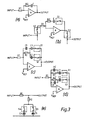
- FIG. 4 shows the block circuit diagram of a phase-locked digital synthesiser according to the invention and intended for use in a burst-mode communications system.
- a voltage controlled oscillator (VCO) 110 receives its input from a feedback loop 112. The VCO output is connected to a digital divider 114 which divides the frequency of the VCO output by an integer N. The integer represents the division ratio and can be varied by a control logic circuit 116.
- the output of the divider 114 is fed to a phase sensitive detector 118, to which is also fed the output of a reference oscillator 120 having a reference frequency f0.
- the phase sensitive detector 118 is connected by change-over switches 122, 124 through one or other of two filter and hold circuits 126, 128 to the input of the voltage control oscillator 110.
- a TR logic signal at a point 130 is low when the terminal is in the receive mode and high when the terminal is in the transmit mode.
- the terminal remains in each mode for 1 millisecond before switching modes. Whilst the terminal is in receive mode any data originating from its user is stored for transmission in the next transmit burst.
- the TR logic signal is fed via an inverter 132 to the circuit 126 and to the control logic circuit 116, and directly to the switches 122, 124 and the circuit 128.
- the control logic circuit 116 selects one division ratio N1 and the feedback loop is completed through the filter and hold circuit 126.
- division ratio N2 is selected, the filter 126 is put into a hold condition where it stores the output voltage existing immediately prior to the transition, and the filter and hold circuit 128 is brought into the feedback loop in place of the filter and hold circuit 126.
- the switching of the circuits 126, 128 is carried out by the switches 122, 124.
- the phase detector 118 is edge-triggered, ie it is sensitive to the rising edges of the pulse trains from the divider 114 and the reference oscillator 120.
- the TR signal changes synchronously with the rising edges of the reference signal from the oscillator 120, the oscillator 120 and the control logic circuit 116 being linked for this purpose.
- the burst length ie the length of time for which the terminal is transmitting or receiving
- the reference frequency f0 from the reference oscillator 120.
- the reference oscillator 120 has a frequency of 100 kHz
- the VCO frequency F1 during receive mode is 800MHz
- the VCO frequency F2 during transmit mode is 810 MHz.
- N1 is then 8000 and N2 8100.
- the division ratio N1 or N2 is set by a register feeding a counter.
- the required division ratio N1 or N2 is fed into the register by the control logic circuit 116, then the division ratio N1 or N2 is supplied to the counter each time this has decremented to zero.
- the division ratio 8000 will be loaded from the register into the counter.
- the counter will then decrement to zero at which point a rising pulse edge will be detected by the phase sensitive detector 118.
- a fresh division ratio N1 (or N2 if the terminal is about to go into transmit mode) will be loaded from the register into the counter.
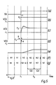
- Figure 5a shows a representative transition at time t1 of the logic signal TR from its receive mode to its transmit mode.
- the vertical lines in Figure 5 represent edges of the reference frequency f0, the temporal spacing of these lines therefore being 10 microseconds because f0 is 100 KHz.
- Figure 5c shows the actual profile of the VCO frequency change, indicating that it takes a finite time for the frequency to change from F1 to F2 and that there is thereafter an overshoot, the frequency settling back to F2 during the second reference cycle after time t1.
- VCO frequency is idealised as a rectangular overshoot of maximum frequency error ⁇ Hz and length ⁇ seconds, as shown in Figure 5d.
- Figure 5e shows the transmitter power transient, illustrating that the new value is achieved after two cycles of the reference frequency.
- Figure 5g illustrates how compensation is achieved.
- the phases of the two inputs to the phase sensitive detector 118 are compared at a sampling time t2.
- This phase comparison is achieved by the phase sensitive detector 134 shown in Figure 4.
- the detector 134 feeds an up/down counter 136 the output of which is fed to the control logic circuit 116 to vary the divider ratio. If the phase error detected by the phase sensitive detector 134 is in the cycle 140 immediately prior to time t2 a correction signal in the form of a division ratio offset ⁇ is incremented by 1. If the phase error is in the cycle 142 immediately succeeding time t2, ⁇ is decremented by 1.
- the counter offset ⁇ is added to the division ratio N2 for the first reference period of the burst only, ie for the first reference cycle following the transition at time t1.
- the counter is loaded with N2 + ⁇ and this has the effect of bringing the divided VCO edges back into synchronism with the reference edges at time t2 and thereafter during that burst.
- ⁇ is stored from transition to transition and that, after adjustment at time t2, the adjusted and updated ⁇ is added to N2 at the start of the first reference cycle following the next transmit/receive transition.
- the value of ⁇ is computed by the first order digital control loop, including the detector 134 and counter 136, as illustrated in Figure 4.
- the adjustment or offset ⁇ is incremented or decremented to the phase error at the sampling time t2 which occurs at the second reference edge after each transition.
- the digital control loop controlling the ⁇ adjustment is in equilibrium, the residual phase error will be within + or - 1 VCO cycle.
- Figure 6a again shows the change in the TR logic signal at a transition from receive mode to transmit mode.
- the vertical lines in Figure 6 represent reference edges, as previously described for Figure 5.
- Figure 6b shows the theoretical VCO frequency with an overshoot ⁇ lasting for a time ⁇ .
- Figure 6c shows the transmitter power transient which occurs shortly after each receive/transmit transition.
- the two inputs to the phase sensitive detector 118 are again sampled at time t2, corresponding to the second reference edge after the transition.
- a division ratio offset ⁇ is decremented by 1 if the phase error occurs in the cycle 144 and the offset ⁇ is incremented by 1 if the phase error occurs in the cycle 146.
- N2 N1 + NI
- N1 is the i.f. offset (expressed as a multiple of the reference frequency).
- f0 100kHz
- N 8550 (mean)
- phase error for a phase error of about 1 cycle we see that ⁇ needs to be of the order of 85. Furthermore the phase adjustment caused by a unit increment of ⁇ is approx. 1/85 cycles or 4.2 degrees. The phase error, and hence peak frequency transient, will therefore be 85 times less than in the embodiment of Figure 5.
- ⁇ is calculated, as indicated, by a first-order digital loop as before, which increments or decrements the counter 136 according to the phase error at the second reference edge following the R/T transition.
- Figure 7 shows the block circuit diagram of a synthesiser for achieving the compensation illustrated diagrammatically in Figure 6. Parts in Figure 7 similar to those in Figure 4 bear the same reference numerals.
- the feedback loop 112 has two capacitors C1 and C2 which are selectively and alternately connected in the feedback loop by switches S3 and S4 connected to a sequence and control logic 152 to which the TR signal is applied. As before, the signal from the feedback loop 112 is applied to the VCO 110 which is connected to the divider 114.
- a switch S1 selects division ratio N1 or N2, the numbers N1 and N2 being in respective stores 154, 156.
- a switch S2 selects ⁇ 1 or ⁇ 2 (or neither) from respective counters 158, 160.
- a two's complementer 162 allows ⁇ 1 or ⁇ 2 to be added to or subtracted from the numbers N1 or N2.
- a digital summer 164 feeds the selected division ratio, with any correction ⁇ 1 or ⁇ 2, to the divider 114.
- the phase sensitive detector 118 has its analogue output fed through a switch S5 to the feedback loop 112.
- the switch S5 allows the output of the detector 118 to be disconnected from the loop 112 for a short period whilst the divider ratio is being changed, as shown in Figure 6e.
Landscapes
- Stabilization Of Oscillater, Synchronisation, Frequency Synthesizers (AREA)
- Oscillators With Electromechanical Resonators (AREA)
- Signal Processing For Digital Recording And Reproducing (AREA)
Priority Applications (1)
| Application Number | Priority Date | Filing Date | Title |
|---|---|---|---|
| AT86305802T ATE77519T1 (de) | 1985-08-02 | 1986-07-29 | In phase verriegelter digitaler synthetisierer. |
Applications Claiming Priority (4)
| Application Number | Priority Date | Filing Date | Title |
|---|---|---|---|
| GB8519521 | 1985-08-02 | ||
| GB8519521 | 1985-08-02 | ||
| GB8613920 | 1986-06-07 | ||
| GB868613920A GB8613920D0 (en) | 1986-06-07 | 1986-06-07 | Phase-locked digital synthesiser |
Publications (3)
| Publication Number | Publication Date |
|---|---|
| EP0211594A2 true EP0211594A2 (fr) | 1987-02-25 |
| EP0211594A3 EP0211594A3 (en) | 1988-11-23 |
| EP0211594B1 EP0211594B1 (fr) | 1992-06-17 |
Family
ID=26289598
Family Applications (1)
| Application Number | Title | Priority Date | Filing Date |
|---|---|---|---|
| EP86305802A Expired EP0211594B1 (fr) | 1985-08-02 | 1986-07-29 | Synthétiseur numérique asservi en phase |
Country Status (4)
| Country | Link |
|---|---|
| US (1) | US4745371A (fr) |
| EP (1) | EP0211594B1 (fr) |
| AT (1) | ATE77519T1 (fr) |
| DE (1) | DE3685695D1 (fr) |
Cited By (10)
| Publication number | Priority date | Publication date | Assignee | Title |
|---|---|---|---|---|
| EP0344856A1 (fr) * | 1988-06-02 | 1989-12-06 | Koninklijke Philips Electronics N.V. | Circuit pour le traitement de signaux vidéo |
| EP0272938A3 (en) * | 1986-12-23 | 1990-03-07 | Nippon Telegraph And Telephone Corporation | Frequency synthesizer |
| EP0404596A3 (fr) * | 1989-06-23 | 1991-03-27 | Nec Corporation | Procédé et appareil de mise en fréquence pour appareil de transmission radio |
| GB2236443A (en) * | 1989-09-01 | 1991-04-03 | Chrontel Inc | Phase-locked loop with sampled-data loop filter |
| EP0453280A1 (fr) * | 1990-04-19 | 1991-10-23 | Nec Corporation | Synthétiseur de fréquence à boucle à verrouillage de phase |
| EP0461358A1 (fr) * | 1990-06-15 | 1991-12-18 | Mitsubishi Denki Kabushiki Kaisha | Synthétiseur de fréquence |
| US5263178A (en) * | 1990-10-05 | 1993-11-16 | Nokie Mobile Phones Ltd. | Procedure for arranging switch-type control in a radio telephone |
| EP0664617A3 (fr) * | 1994-01-19 | 1996-02-14 | Japan Radio Co Ltd | Synthétiseur à PLL. |
| US6396353B1 (en) | 1999-06-30 | 2002-05-28 | Infineon Technologies Ag | PLL frequency synthesizer operated with reduced settling time constant during frequency changeover |
| GB2380340A (en) * | 2001-09-14 | 2003-04-02 | Nec Corp | PLL synthesiser in a cellular phone |
Families Citing this family (18)
| Publication number | Priority date | Publication date | Assignee | Title |
|---|---|---|---|---|
| US4885553A (en) * | 1988-11-30 | 1989-12-05 | Motorola, Inc. | Continuously adaptive phase locked loop synthesizer |
| US4920320A (en) * | 1988-12-19 | 1990-04-24 | Motorola, Inc. | Phase locked loop with optimally controlled bandwidth |
| US4951004A (en) * | 1989-03-17 | 1990-08-21 | John Fluke Mfg. Co., Inc. | Coherent direct digital synthesizer |
| US5081705A (en) * | 1989-06-29 | 1992-01-14 | Rockwell International Corp. | Communication system with external reference signal processing capability |
| US4992743A (en) * | 1989-11-15 | 1991-02-12 | John Fluke Mfg. Co., Inc. | Dual-tone direct digital synthesizer |
| JP2748676B2 (ja) * | 1990-09-19 | 1998-05-13 | 日本電気株式会社 | Pll回路 |
| US5146187A (en) * | 1991-07-01 | 1992-09-08 | Ericsson Ge Mobile Communications Inc. | Synthesizer loop filter for scanning receivers |
| US5371480A (en) * | 1992-12-04 | 1994-12-06 | Telefonaktiebolaget L M Ericsson | Step controlled signal generator |
| JP2616582B2 (ja) * | 1994-05-09 | 1997-06-04 | 日本電気株式会社 | Pll周波数シンセサイザ |
| FR2734967B1 (fr) * | 1995-05-31 | 1997-07-04 | Cit Alcatel | Procede de verrouillage de phase et boucle appliquant ce procede |
| US6081143A (en) * | 1997-09-26 | 2000-06-27 | Sun Microsystems, Inc. | Frequency comparison and generation in an integrated processor |
| US6112068A (en) * | 1997-12-22 | 2000-08-29 | Texas Instruments Incorporated | Phase-locked loop circuit with switchable outputs for multiple loop filters |
| US6456887B1 (en) * | 2000-12-14 | 2002-09-24 | Medtronic, Inc. | Low energy consumption RF telemetry control for an implantable medical device |
| TWI224428B (en) * | 2002-07-19 | 2004-11-21 | Sun Microsystems Inc | Loop filter capacitor leakage current control |
| US8412116B1 (en) * | 2002-12-20 | 2013-04-02 | Qualcomm Incorporated | Wireless transceiver |
| DE102004030841A1 (de) * | 2004-06-25 | 2006-01-26 | Siemens Ag | Verringerung der Einschwingzeit und Kompensation von Phasenfeldern von auf Phasenregelkreisen basierenden Frequenzsynthesizern |
| DE102004047871A1 (de) * | 2004-10-01 | 2006-04-06 | Deutsche Thomson-Brandt Gmbh | Signal-Eingangsschaltung |
| WO2010020911A1 (fr) * | 2008-08-21 | 2010-02-25 | Nxp B.V. | Synthétiseur de fréquence et configuration pour un taux de saut de fréquence amélioré |
Family Cites Families (2)
| Publication number | Priority date | Publication date | Assignee | Title |
|---|---|---|---|---|
| US3729688A (en) * | 1971-12-15 | 1973-04-24 | Motorola Inc | Oscillator with switchable filter control voltage input for rapidly switching to discrete frequency outputs |
| US4629999A (en) * | 1983-12-27 | 1986-12-16 | North American Philips Corp. | Phase-locked loop capable of generating a plurality of stable frequency signals |
-
1986
- 1986-07-23 US US06/888,798 patent/US4745371A/en not_active Expired - Fee Related
- 1986-07-29 EP EP86305802A patent/EP0211594B1/fr not_active Expired
- 1986-07-29 DE DE8686305802T patent/DE3685695D1/de not_active Expired - Lifetime
- 1986-07-29 AT AT86305802T patent/ATE77519T1/de not_active IP Right Cessation
Cited By (13)
| Publication number | Priority date | Publication date | Assignee | Title |
|---|---|---|---|---|
| EP0272938A3 (en) * | 1986-12-23 | 1990-03-07 | Nippon Telegraph And Telephone Corporation | Frequency synthesizer |
| EP0344856A1 (fr) * | 1988-06-02 | 1989-12-06 | Koninklijke Philips Electronics N.V. | Circuit pour le traitement de signaux vidéo |
| EP0404596A3 (fr) * | 1989-06-23 | 1991-03-27 | Nec Corporation | Procédé et appareil de mise en fréquence pour appareil de transmission radio |
| GB2236443B (en) * | 1989-09-01 | 1993-08-11 | Chrontel Inc | Phase-locked loop |
| GB2236443A (en) * | 1989-09-01 | 1991-04-03 | Chrontel Inc | Phase-locked loop with sampled-data loop filter |
| EP0453280A1 (fr) * | 1990-04-19 | 1991-10-23 | Nec Corporation | Synthétiseur de fréquence à boucle à verrouillage de phase |
| EP0461358A1 (fr) * | 1990-06-15 | 1991-12-18 | Mitsubishi Denki Kabushiki Kaisha | Synthétiseur de fréquence |
| US5263178A (en) * | 1990-10-05 | 1993-11-16 | Nokie Mobile Phones Ltd. | Procedure for arranging switch-type control in a radio telephone |
| EP0664617A3 (fr) * | 1994-01-19 | 1996-02-14 | Japan Radio Co Ltd | Synthétiseur à PLL. |
| US6396353B1 (en) | 1999-06-30 | 2002-05-28 | Infineon Technologies Ag | PLL frequency synthesizer operated with reduced settling time constant during frequency changeover |
| GB2380340A (en) * | 2001-09-14 | 2003-04-02 | Nec Corp | PLL synthesiser in a cellular phone |
| GB2380340B (en) * | 2001-09-14 | 2004-03-17 | Nec Corp | PLL synthesizer for a cellular phone |
| US6727763B2 (en) | 2001-09-14 | 2004-04-27 | Nec Corporation | PLL synthesizer in a cellular phone |
Also Published As
| Publication number | Publication date |
|---|---|
| DE3685695D1 (de) | 1992-07-23 |
| US4745371A (en) | 1988-05-17 |
| EP0211594B1 (fr) | 1992-06-17 |
| ATE77519T1 (de) | 1992-07-15 |
| EP0211594A3 (en) | 1988-11-23 |
Similar Documents
| Publication | Publication Date | Title |
|---|---|---|
| EP0211594B1 (fr) | Synthétiseur numérique asservi en phase | |
| EP0453280B1 (fr) | Synthétiseur de fréquence à boucle à verrouillage de phase | |
| US5175729A (en) | Radio with fast lock phase-locked loop | |
| US5424689A (en) | Filtering device for use in a phase locked loop controller | |
| US4516083A (en) | Fast lock PLL having out of lock detector control of loop filter and divider | |
| EP0471506B1 (fr) | Boucle de verrouillage de phase utilisant un signal de référence de fréquence multiple et non entier | |
| EP0669722B1 (fr) | Circuit à PLL présentant un temps de synchronisation réduit | |
| US5910753A (en) | Direct digital phase synthesis | |
| US5661440A (en) | PLL frequency synthesizer employing plural control frequencies to minimize overshoot | |
| EP0560525B1 (fr) | Synthétiseur de fréquence | |
| WO1999000902A1 (fr) | Dispositif de communications a synthetiseur de correction de frequence, et principe de mise en oeuvre | |
| CA1054232A (fr) | Detecteur de phase a gamme lineaire de 360.degree. pour trains d'impulsions periodiques et aperiodiques | |
| WO2000031874A1 (fr) | Boucle a phase asservie activant une commutation lisse de la largeur de bande de la boucle | |
| KR20070009749A (ko) | 주파수 합성기의 적응 주파수 조정장치 | |
| US5150082A (en) | Center frequency calibration for DC coupled frequency modulation in a phase-locked loop | |
| EP0625292B1 (fr) | Synthetiseur de frequences permettant un retour rapide | |
| JPH0473328B2 (fr) | ||
| US5408202A (en) | Phase lock loop having a lock acquisition mode and method of operation therefor | |
| US6035182A (en) | Single counter dual modulus frequency division apparatus | |
| EP0565362B1 (fr) | Accord automatique de fréquence avec synthétiseur de fréquence | |
| EP0895674B1 (fr) | Sequenage d'une emission | |
| AU615848B2 (en) | Analogue/digital phase locked loop | |
| CA2389160C (fr) | Regenerateur de rythme et de donnees pour differents debits de donnees | |
| US3781696A (en) | Regenerator for generating a pulse series which is to be stabilized on an incoming impulse series | |
| CN1717861B (zh) | 使用频率偏移补偿的调制器和方法 |
Legal Events
| Date | Code | Title | Description |
|---|---|---|---|
| PUAI | Public reference made under article 153(3) epc to a published international application that has entered the european phase |
Free format text: ORIGINAL CODE: 0009012 |
|
| AK | Designated contracting states |
Kind code of ref document: A2 Designated state(s): AT BE CH DE FR GB IT LI LU NL SE |
|
| PUAL | Search report despatched |
Free format text: ORIGINAL CODE: 0009013 |
|
| AK | Designated contracting states |
Kind code of ref document: A3 Designated state(s): AT BE CH DE FR GB IT LI LU NL SE |
|
| 17P | Request for examination filed |
Effective date: 19881219 |
|
| 17Q | First examination report despatched |
Effective date: 19910219 |
|
| RAP1 | Party data changed (applicant data changed or rights of an application transferred) |
Owner name: LIBERA DEVELOPMENTS LIMITED |
|
| GRAA | (expected) grant |
Free format text: ORIGINAL CODE: 0009210 |
|
| AK | Designated contracting states |
Kind code of ref document: B1 Designated state(s): AT BE CH DE FR GB IT LI LU NL SE |
|
| PG25 | Lapsed in a contracting state [announced via postgrant information from national office to epo] |
Ref country code: IT Free format text: LAPSE BECAUSE OF FAILURE TO SUBMIT A TRANSLATION OF THE DESCRIPTION OR TO PAY THE FEE WITHIN THE PRESCRIBED TIME-LIMIT;WARNING: LAPSES OF ITALIAN PATENTS WITH EFFECTIVE DATE BEFORE 2007 MAY HAVE OCCURRED AT ANY TIME BEFORE 2007. THE CORRECT EFFECTIVE DATE MAY BE DIFFERENT FROM THE ONE RECORDED. Effective date: 19920617 Ref country code: LI Effective date: 19920617 Ref country code: DE Effective date: 19920617 Ref country code: NL Effective date: 19920617 Ref country code: SE Effective date: 19920617 Ref country code: AT Effective date: 19920617 Ref country code: BE Effective date: 19920617 Ref country code: CH Effective date: 19920617 |
|
| REF | Corresponds to: |
Ref document number: 77519 Country of ref document: AT Date of ref document: 19920715 Kind code of ref document: T |
|
| REF | Corresponds to: |
Ref document number: 3685695 Country of ref document: DE Date of ref document: 19920723 |
|
| PG25 | Lapsed in a contracting state [announced via postgrant information from national office to epo] |
Ref country code: LU Free format text: LAPSE BECAUSE OF NON-PAYMENT OF DUE FEES Effective date: 19920731 |
|
| ET | Fr: translation filed | ||
| REG | Reference to a national code |
Ref country code: CH Ref legal event code: PL |
|
| REG | Reference to a national code |
Ref country code: GB Ref legal event code: 732 |
|
| NLV1 | Nl: lapsed or annulled due to failure to fulfill the requirements of art. 29p and 29m of the patents act | ||
| REG | Reference to a national code |
Ref country code: FR Ref legal event code: TP |
|
| PLBE | No opposition filed within time limit |
Free format text: ORIGINAL CODE: 0009261 |
|
| STAA | Information on the status of an ep patent application or granted ep patent |
Free format text: STATUS: NO OPPOSITION FILED WITHIN TIME LIMIT |
|
| 26N | No opposition filed | ||
| PGFP | Annual fee paid to national office [announced via postgrant information from national office to epo] |
Ref country code: GB Payment date: 19960625 Year of fee payment: 11 |
|
| PGFP | Annual fee paid to national office [announced via postgrant information from national office to epo] |
Ref country code: FR Payment date: 19960704 Year of fee payment: 11 |
|
| PG25 | Lapsed in a contracting state [announced via postgrant information from national office to epo] |
Ref country code: GB Free format text: LAPSE BECAUSE OF NON-PAYMENT OF DUE FEES Effective date: 19970729 |
|
| GBPC | Gb: european patent ceased through non-payment of renewal fee |
Effective date: 19970729 |
|
| PG25 | Lapsed in a contracting state [announced via postgrant information from national office to epo] |
Ref country code: FR Free format text: LAPSE BECAUSE OF NON-PAYMENT OF DUE FEES Effective date: 19980331 |
|
| REG | Reference to a national code |
Ref country code: FR Ref legal event code: ST |