EP0212045A2 - Adaptation d'un dispositif d'affichage ou d'évaluation à un capteur - Google Patents
Adaptation d'un dispositif d'affichage ou d'évaluation à un capteur Download PDFInfo
- Publication number
- EP0212045A2 EP0212045A2 EP86101552A EP86101552A EP0212045A2 EP 0212045 A2 EP0212045 A2 EP 0212045A2 EP 86101552 A EP86101552 A EP 86101552A EP 86101552 A EP86101552 A EP 86101552A EP 0212045 A2 EP0212045 A2 EP 0212045A2
- Authority
- EP
- European Patent Office
- Prior art keywords
- sensor
- detection
- plug
- resistor
- voltage
- Prior art date
- Legal status (The legal status is an assumption and is not a legal conclusion. Google has not performed a legal analysis and makes no representation as to the accuracy of the status listed.)
- Withdrawn
Links
Images

Classifications
-
- G—PHYSICS
- G01—MEASURING; TESTING
- G01D—MEASURING NOT SPECIALLY ADAPTED FOR A SPECIFIC VARIABLE; ARRANGEMENTS FOR MEASURING TWO OR MORE VARIABLES NOT COVERED IN A SINGLE OTHER SUBCLASS; TARIFF METERING APPARATUS; MEASURING OR TESTING NOT OTHERWISE PROVIDED FOR
- G01D3/00—Indicating or recording apparatus with provision for the special purposes referred to in the subgroups
-
- G—PHYSICS
- G01—MEASURING; TESTING
- G01B—MEASURING LENGTH, THICKNESS OR SIMILAR LINEAR DIMENSIONS; MEASURING ANGLES; MEASURING AREAS; MEASURING IRREGULARITIES OF SURFACES OR CONTOURS
- G01B2210/00—Aspects not specifically covered by any group under G01B, e.g. of wheel alignment, caliper-like sensors
- G01B2210/60—Unique sensor identification
Definitions
- the invention relates to a device for automatically adapting the measuring range of a display or evaluation device (hereinafter simply called “device”) to the range of output voltages of a sensor for a physical variable.
- the physical quantity to be measured can be arbitrary, e.g. B. a pressure, a temperature, a pH-Wart or any electrical quantity.
- a display device only the size to be measured, e.g. B. indicates by a pointer deflection or by a digital display
- an evaluation device (with or without a display) in response to a measurement signal entered him to accomplish something, z. B. trigger an alarm signal or activate a circuit that in turn can have any task.
- the adaptation is not a problem.
- the situation is different if different types of sensors are to be used, which emit measurement signals of very different sizes and if all are to be connected alternately to the same device or if the same sensor is to be connected alternately to one or the other device and similar variants more.
- the present invention is intended to automatically carry out the required adaptation when a sensor is connected to a device. This object is achieved by the invention according to claim 1.
- a connector is used to connect the sensor to the device.
- Each of the devices in question is provided with one part (e.g. with pins) of the connector, while each of the sensors is provided with the other part (e.g. with sockets) of the connector.
- Each of the sensors can thus be connected to each of the devices.
- the detection resistor arranged on the sensor side and the detection circuit arranged on the device side are used for the automatic adaptation and only take effect after a device has been connected to a sensor.
- an adaptation can be accomplished using a series connection of two sections.
- One section corresponds to the internal resistance of the device or is equal to this internal resistance
- the other which is assigned to the sensor, corresponds to a detection resistance or is equal to the detection resistance.
- This detection resistor has a certain typical size for each sensor. In the simplest case, when all the devices in question have the same internal resistance, the size of the detection resistance itself ensures the correct adjustment.
- the size of the detection resistance can be determined from the device after connecting the sensor.
- a detection line which is independent of the measurement signal line is then preferably used.
- Matching the internal resistance of the device can be turned on according to claim 5, one of several matching resistors, the z. B. are connected as shunts parallel to the input of the device.
- a step comparator can be used according to claim 6, which is connected to the detection line.
- the detection of the sensor used can be carried out in the event that the sensor and device are operated with alternating current.
- encryption can be achieved in a different way.
- a comparator on the sensor side normally does not emit an output signal via a detection resistor, but only when potentials at its inputs are changed.
- This can be from a voltage stabilizer arranged on the device side, which serves as a voltage source for the sensor and whose output voltage assumes a different, in particular higher, value shortly after switching on. This higher value changes the potentials at the inputs of the comparator in the sensor so that the comparator briefly outputs an output signal via the detection resistor into the detection line.
- an encrypted adaptation can be carried out without detection resistance in such a way that some, in particular binary, coding switches are provided on the sensor side and a decoder, in particular a binary decimal decoder on the device side, which then ensures the setting of the appropriate adaptation resistance.
- FIGS 1 to 7 show circuits (or their respective essential parts) of various devices for automatic measuring range adjustment.
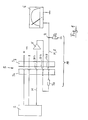
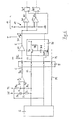
- the sensor is marked with S, the device with G and the connector with 5.
- the sensor can either by itself, for. B. be supplied with voltage by its own power supply, or as in all embodiments, via the connector 5 from the device. Every single socket and every single plug of the connector is called "plug element St ". Ri always denotes the internal resistance of the device, Re the detection resistance of the sensor.
- a line carrying the measurement signal is always designated M, regardless of whether it belongs to the sensor or the device and whether it carries an unamplified or already amplified measurement signal. Instead of the only one shown everywhere, there can be two parallel detection lines. All sections of a line coming from the detection resistor Re are always labeled E, regardless of whether they are present on the sensor side, device side, before or after an amplifier.
- the sensor is supplied with DC voltage.
- the measurement signal line M from the sensor leads via a plug element St3 to the input of an amplifier V arranged in the device G, the output of which leads to a plug element St4.
- the plug-in elements St4 and St5 are through the bay Resistance bridged.
- a line M, E which is both a measurement signal line and a detection line, leads from the plug element St5 to the device G, the internal resistance Ri of which is shown separately.
- the detection resistor Re can be arranged in the sensor itself or in the sensor plug-in part. The ratio of the resistances Re / Ri is decisive for the adaptation. These two resistors together form a voltage divider 10.
- a tap 9 between the two resistors is the signal input of the device G. (Ri is the internal resistance of the device.)
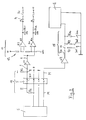
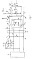
- the connector is shown in simplified form in FIG. 2 and the following figures.
- measurement signal line M and detection line E are separated from one another.
- DC voltage is used for the supply.
- the detection resistor Re arranged on the sensor side and the internal resistance Ri of the device form a voltage divider 10.
- the detection resistor Re leads from the positive pole of the voltage supply via plug elements St1 to the tap 9 of the voltage divider. This tap is connected to the input of an amplifier V1.
- the amplifier output leads to a stage comparator, which is designated as a whole by 11 and has a digital, in particular decimal output.
- the right end of the detection line E is connected to the one input of a series of comparators K1 to Kn, only two of which are shown here.
- the other inputs of these comparators are located at the junctures between the individual resistors (there are more resistors than shown) of a voltage part 12 which bridges the voltage source.
- output signals can appear at one or more of the comparators In the case of simple comparators, either none, some of the comparators or all of them. If window comparators are used, an output signal only occurs at a selected comparator, namely only at the one at which the input voltage difference falls within a certain range, the "window".
- the outputs of the comparators are connected to the positive pole via a series resistor Rv.
- a light-emitting diode 14 can lie in each of these lines. The LEDs can be used to display the physical quantity to be measured and to display the set measuring range and can each illuminate a window with an inscription such as "pressure", "temperature” etc.
- a relay R11 to Rln is located between the outputs A1 to On and ground. When using window comparators, only one of these relays is turned on, and this case will be used for the further description.
- the measurement signal line contains an amplifier V2 on the device side and then a voltage divider 15 with a tap 17 which is connected to the positive input of the device G. Between this tap and the output of the amplifier V2 there is a series resistor Rm (the measurement signal line) which forms one branch of the voltage divider 15.
- the ratios R1 / Rm to Rn / Rm of the resistors are decisive for the adaptation.
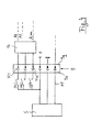
- the sensor is supplied with AC voltage.
- a voltage divider 10 is formed which contains the detection resistor Re on the sensor side and the internal resistance Ri of the device on the device side. Its tap 9 is fed to the negative input of an operational amplifier Vo.
- the voltage source is bridged by two equally large resistors Rs and Rt, the common connection point of which is connected to the positive input of the operational amplifier Vo.
- a feedback resistor Rr leads to its signal input in the usual way.
- H. tap 9 The output signal of the operational amplifier is rectified by a diode D1 with capacitor C1. The rectified signal is fed to an amplifier V1 and its output signal in turn to a stage comparator. The rest of the circuit and its mode of operation are the same as shown in FIG. 2 and described with reference to FIG.
- the resistors shown in FIG. 3 need not be ohmic resistors, but can be very generally impedances and contain capacitors, coils and / or semiconductors.
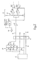
- the sensor S is supplied with direct voltage.
- the adaptation can be achieved via coding and decoding.
- a number of z. B. eight coding switches Sk1, Sk2 to Skn are provided, which are all connected to the positive pole. The other side of each of the switches leads to one of the plug elements St1 to Stn.
- Device egg A binary decimal decoder 16 is provided which has n inputs. Depending on which of the switches Sk1 to Skn are closed, a signal is present at one of the decimal outputs A1 to Am. As described with reference to FIG. 2, one of the matching resistors R1 to Rn of the device is accordingly switched on. The measurement signal is fed to the device as described with reference to FIG. 2.
- the ratio of two detection resistors Re1 and Re2 can be encoded.
- the resistance ratio can then only be determined briefly, in particular when the sensor is plugged in or when the voltage supply is switched on.
- the detection line E can be grounded between the connector 5 and the amplifier V1 by a changeover switch Sx.
- the switch can be closed by a monostable multivibrator (Monoflop Mf1 "Power Reset") for a short time.
- the Monoflop Mf1 can be started either manually or automatically or after applying the supply voltage. It returns after a pulse (the first switching time) of z. B.
- a tap 22 is connected to ground between the two detection resistors Re1 and Re2.
- the upper side of the semiconductor circuit 20 in FIG. 5 is connected to plus.
- a transistor T1 now becomes conductive via the resistor Re2, a resistor R4 and a capacitor C1.
- the transistor T2 becomes conductive via a resistor R5 which is connected to the collector of this transistor and the base of a transistor T2. From now on, the capacitor C1 is charged.
- the detection is connected in series resistances Re1 and Re2 approximately at the full supply voltage.
- a signal appears in the detection line E, the voltage of which is given by the ratio of the two detection resistors.
- the amplifier V1 After passing through the amplifier V1, it is evaluated in the manner described below, and thus serves to set one of the matching resistors R1 to Rn (FIG. 2) for the device.
- the changeover switch Sx is brought back into its drawn position by the monaflop Mf1, which on the one hand separates the tap 22 from the ground and on the other hand starts a monoflop Mf2 which has a dynamic or clock input. Its output is connected to a dynamic input from memories Sp1 to Spn. A further input of the memory provided for a useful signal is connected to the output of one of the comparators K1 to Kn.
- the monoflop Mf2 remains during a second switching time of e.g. B. active for half a second and activates the memory Sp1 to Spn during this time. As a result, these memories take over the output signal or the output signals which occur at the outputs A1 to An of the comparators K1 to Kn.
- the signals occurring at the outputs of the memories are used in the manner described with reference to FIG. 2 to switch on one of the matching resistors R1 to Rn.
- Detecting the ratio of the detection resistors Rel / Re2 is therefore only possible as long as the capacitor C1 contains a charge. It is therefore not possible to measure the resistance ratio from the outside without a device with a suitable interrogation circuit.
- the value of the detection resistor Re cannot normally be determined from the outside.
- the input Eg1 of a comparator K is normally at a lower potential than its input Eg2. Therefore, no signal occurs at the output of the comparator K and also in the detection line E.
- One input Eg1 of the comparator K is connected to a tap 21 of a series circuit 34 composed of two identical resistors Ra and Rb, the other ends of which are connected to the two poles of the voltage source (supply line VL and ground).
- the second input (Eg2) of the comparator is connected to a tap 23 of a series circuit 35 comprising a reference diode 24 and a resistor Rc. The outer ends of this series circuit 35 are also connected to the supply voltage.
- the reference voltage of the reference diode is dimensioned such that there is normally a higher potential at the Eg2 input than at the Eg1 input, so that the comparator does not normally emit an output signal.
- the circuit is activated by briefly increasing the supply voltage.
- a voltage stabilizer 26 with a transistor T8, a resistor R8 and a Zener diode D8 is used for this purpose.
- the switch can be opened briefly by hand or when the device is switched on and then ensures a definite voltage change at the output of the voltage stabilizer 26 in the line VL. With the switch Sa8 open, the zener diode can no longer work.
- This voltage change briefly increases the potential at input Eg1 of comparator K. It becomes higher than that at the input Eg2, and a detection signal thus occurs at the output of the comparator and after the detection resistor Re in the detection line E, which makes it possible to determine the ratio of the detection resistance Re to the internal resistance Ri.
- a button 30 achieves two things simultaneously when the device and sensor are switched on. On the one hand, switch S8 briefly generates an overvoltage in voltage constant holder 26. On the other hand, when the button 30 is closed, a pulse is given to the clock input of each of the memories, so that the memories are briefly activated.
- the detection signal is again fed to a stage comparator 11, as was described above with reference to FIG. 2.
- One or more output signals of the stage comparator are stored in the memories Sp1 to Spn and, as described, serve to switch on one of the matching resistors R1 to Rn for the device.
- the detection resistance Re has a different position here. It establishes a connection from the output of the comparator K to the measurement signal line M. After an amplifier V2 for the measurement signal and the detection signal, a line 28 leads to the input of the stage comparator 11. Otherwise, this circuit operates like that according to FIG. 6.
Landscapes
- Physics & Mathematics (AREA)
- General Physics & Mathematics (AREA)
- Arrangements For Transmission Of Measured Signals (AREA)
- Measurement Of Current Or Voltage (AREA)
- Indication And Recording Devices For Special Purposes And Tariff Metering Devices (AREA)
- Testing Or Calibration Of Command Recording Devices (AREA)
Applications Claiming Priority (2)
| Application Number | Priority Date | Filing Date | Title |
|---|---|---|---|
| DE3524770 | 1985-07-11 | ||
| DE3524770 | 1985-07-11 |
Publications (2)
| Publication Number | Publication Date |
|---|---|
| EP0212045A2 true EP0212045A2 (fr) | 1987-03-04 |
| EP0212045A3 EP0212045A3 (fr) | 1988-01-27 |
Family
ID=6275501
Family Applications (1)
| Application Number | Title | Priority Date | Filing Date |
|---|---|---|---|
| EP86101552A Withdrawn EP0212045A3 (fr) | 1985-07-11 | 1986-02-06 | Adaptation d'un dispositif d'affichage ou d'évaluation à un capteur |
Country Status (1)
| Country | Link |
|---|---|
| EP (1) | EP0212045A3 (fr) |
Cited By (5)
| Publication number | Priority date | Publication date | Assignee | Title |
|---|---|---|---|---|
| DE3826767A1 (de) * | 1988-08-06 | 1990-02-08 | Kostal Leopold Gmbh & Co Kg | Sensoreinrichtung |
| WO1994008215A1 (fr) * | 1992-09-29 | 1994-04-14 | Endress U. Hauser Gmbh U. Co. | Dispositif de detection et/ou de controle d'un niveau predetermine dans un reservoir |
| EP0607464A1 (fr) * | 1992-09-11 | 1994-07-27 | Societe Marechaux Dubost Instruments S.A. | Dispositif d'acquisition de mesures multifonction |
| EP1271167B1 (fr) * | 2002-04-06 | 2004-02-18 | Agilent Technologies, Inc. (a Delaware corporation) | Système électrique pour tester des canaux d'un système de communication |
| EP1271168B1 (fr) * | 2002-04-06 | 2004-12-15 | Agilent Technologies, Inc. (a Delaware corporation) | Système électrique pour tester les canaux d'un système de communication |
Family Cites Families (3)
| Publication number | Priority date | Publication date | Assignee | Title |
|---|---|---|---|---|
| US3464012A (en) * | 1967-02-17 | 1969-08-26 | Webb James E | Automatic signal range selector for metering devices |
| US3577076A (en) * | 1968-09-05 | 1971-05-04 | Ibm | Automatic range scale selection apparatus for a measuring device |
| US3943440A (en) * | 1974-10-03 | 1976-03-09 | Hewlett-Packard Company | Sensitivity coding circuit for an electronic instrument |
-
1986
- 1986-02-06 EP EP86101552A patent/EP0212045A3/fr not_active Withdrawn
Cited By (8)
| Publication number | Priority date | Publication date | Assignee | Title |
|---|---|---|---|---|
| DE3826767A1 (de) * | 1988-08-06 | 1990-02-08 | Kostal Leopold Gmbh & Co Kg | Sensoreinrichtung |
| EP0607464A1 (fr) * | 1992-09-11 | 1994-07-27 | Societe Marechaux Dubost Instruments S.A. | Dispositif d'acquisition de mesures multifonction |
| WO1994008215A1 (fr) * | 1992-09-29 | 1994-04-14 | Endress U. Hauser Gmbh U. Co. | Dispositif de detection et/ou de controle d'un niveau predetermine dans un reservoir |
| US5717383A (en) * | 1992-09-29 | 1998-02-10 | Endress + Hauser Gmbh + Co. | Device for determining and/or monitoring a predetermined level of contents in a container |
| EP1271167B1 (fr) * | 2002-04-06 | 2004-02-18 | Agilent Technologies, Inc. (a Delaware corporation) | Système électrique pour tester des canaux d'un système de communication |
| EP1271168B1 (fr) * | 2002-04-06 | 2004-12-15 | Agilent Technologies, Inc. (a Delaware corporation) | Système électrique pour tester les canaux d'un système de communication |
| US6844746B2 (en) | 2002-04-06 | 2005-01-18 | Agilent Technologies, Inc. | Electrical system like a testing system for testing the channels of a communication system |
| US7149286B2 (en) | 2002-04-06 | 2006-12-12 | Heinz Nuessle | Electrical system like a system for testing the channels of a communication system |
Also Published As
| Publication number | Publication date |
|---|---|
| EP0212045A3 (fr) | 1988-01-27 |
Similar Documents
| Publication | Publication Date | Title |
|---|---|---|
| EP0011711B1 (fr) | Dispositif de test pour l'indication par paliers d'une tension à mesurer | |
| DE2356518B2 (de) | Batterie-Ladegerät | |
| DE2012900A1 (de) | Selbsttätig arbeitende Prüfvorrichtung für mehradrige elektrische Kabel | |
| DE2703880C3 (de) | Elektrisches Prüfgerät mit akustischer, quantitativer Analoganzeige für Widerstand und Spannung | |
| CH619786A5 (fr) | ||
| DE112017004536T5 (de) | MPS-Erzeugungssystem und -verfahren | |
| DE2809596A1 (de) | Schaltungsanordnung zur erfassung von erdschluessen zweiadriger meldeleitungen | |
| EP0212045A2 (fr) | Adaptation d'un dispositif d'affichage ou d'évaluation à un capteur | |
| DE68924829T2 (de) | Verfahren und Vorrichtung um die aufgenommene Leistung einer Telefonschnittstellenschaltung im Ruhe-Zustand gering zu halten. | |
| EP0052220B1 (fr) | Méthode et dispositif de mesure de résistance dans une ligne de signalisation | |
| DE4224266C1 (de) | Überwachungseinrichtung für mehrere elektrische Schalter | |
| DE3027398A1 (de) | Elektrische anzeigevorrichtung ohne hilfsenergie | |
| DE3344363C2 (fr) | ||
| DE3225081A1 (de) | Verfahren und einrichtung zur automatischen abfrage des meldermesswerts und der melderkennung in einer gefahrenmeldeanlage | |
| DE3915880C2 (fr) | ||
| DE2729271A1 (de) | Geraet zur durchfuehrung von einordnungs-tests, insbesondere von farbeinordnungs-sehtests | |
| DE2607606C2 (de) | Potentialprüfer | |
| DE3924693C2 (fr) | ||
| DE3701070C2 (fr) | ||
| DE3813883C2 (fr) | ||
| DE3006011C2 (fr) | ||
| DE2364424C2 (de) | Prüfgerät für bipolare und Feldeffekt-Transistoren | |
| AT397591B (de) | Messgerät zur erfassung und anzeige verschiedener messwerte, insbesondere zur messwerterfassung in netzwerken von wählsystemen | |
| DE2060884C3 (de) | Prüfeinrichtung zum Anzeigen der Polarität bzw. der Phasenlage von elektrischen Potentialen | |
| DE3037973C2 (de) | Schaltungsanordnung zum Erkennen des Schleifenschlusses für eine Teilnehmerschaltung in einer Fernsprechanlage |
Legal Events
| Date | Code | Title | Description |
|---|---|---|---|
| PUAI | Public reference made under article 153(3) epc to a published international application that has entered the european phase |
Free format text: ORIGINAL CODE: 0009012 |
|
| AK | Designated contracting states |
Kind code of ref document: A2 Designated state(s): AT CH DE FR GB IT LI NL SE |
|
| PUAL | Search report despatched |
Free format text: ORIGINAL CODE: 0009013 |
|
| RHK1 | Main classification (correction) |
Ipc: G01R 15/08 |
|
| AK | Designated contracting states |
Kind code of ref document: A3 Designated state(s): AT CH DE FR GB IT LI NL SE |
|
| 17P | Request for examination filed |
Effective date: 19880109 |
|
| 17Q | First examination report despatched |
Effective date: 19900713 |
|
| STAA | Information on the status of an ep patent application or granted ep patent |
Free format text: STATUS: THE APPLICATION HAS BEEN WITHDRAWN |
|
| 18W | Application withdrawn |
Withdrawal date: 19911216 |