EP0212253B1 - Verfahren und Einrichtung zur Reinigung, Aktivierung und/oder Metallisierung von Bohrlöchern in horizontal geführten Leiterplatten - Google Patents
Verfahren und Einrichtung zur Reinigung, Aktivierung und/oder Metallisierung von Bohrlöchern in horizontal geführten Leiterplatten Download PDFInfo
- Publication number
- EP0212253B1 EP0212253B1 EP86109731A EP86109731A EP0212253B1 EP 0212253 B1 EP0212253 B1 EP 0212253B1 EP 86109731 A EP86109731 A EP 86109731A EP 86109731 A EP86109731 A EP 86109731A EP 0212253 B1 EP0212253 B1 EP 0212253B1
- Authority
- EP
- European Patent Office
- Prior art keywords
- jet
- accordance
- circuit board
- transport
- circuit boards
- Prior art date
- Legal status (The legal status is an assumption and is not a legal conclusion. Google has not performed a legal analysis and makes no representation as to the accuracy of the status listed.)
- Expired - Lifetime
Links
Images

Classifications
-
- H—ELECTRICITY
- H05—ELECTRIC TECHNIQUES NOT OTHERWISE PROVIDED FOR
- H05K—PRINTED CIRCUITS; CASINGS OR CONSTRUCTIONAL DETAILS OF ELECTRIC APPARATUS; MANUFACTURE OF ASSEMBLAGES OF ELECTRICAL COMPONENTS
- H05K3/00—Apparatus or processes for manufacturing printed circuits
-
- H—ELECTRICITY
- H05—ELECTRIC TECHNIQUES NOT OTHERWISE PROVIDED FOR
- H05K—PRINTED CIRCUITS; CASINGS OR CONSTRUCTIONAL DETAILS OF ELECTRIC APPARATUS; MANUFACTURE OF ASSEMBLAGES OF ELECTRICAL COMPONENTS
- H05K3/00—Apparatus or processes for manufacturing printed circuits
- H05K3/0085—Apparatus for treatments of printed circuits with liquids not provided for in groups H05K3/02 - H05K3/46; conveyors and holding means therefor
- H05K3/0088—Apparatus for treatments of printed circuits with liquids not provided for in groups H05K3/02 - H05K3/46; conveyors and holding means therefor for treatment of holes
-
- H—ELECTRICITY
- H05—ELECTRIC TECHNIQUES NOT OTHERWISE PROVIDED FOR
- H05K—PRINTED CIRCUITS; CASINGS OR CONSTRUCTIONAL DETAILS OF ELECTRIC APPARATUS; MANUFACTURE OF ASSEMBLAGES OF ELECTRICAL COMPONENTS
- H05K2203/00—Indexing scheme relating to apparatus or processes for manufacturing printed circuits covered by H05K3/00
- H05K2203/02—Details related to mechanical or acoustic processing, e.g. drilling, punching, cutting, using ultrasound
- H05K2203/0285—Using ultrasound, e.g. for cleaning, soldering or wet treatment
-
- H—ELECTRICITY
- H05—ELECTRIC TECHNIQUES NOT OTHERWISE PROVIDED FOR
- H05K—PRINTED CIRCUITS; CASINGS OR CONSTRUCTIONAL DETAILS OF ELECTRIC APPARATUS; MANUFACTURE OF ASSEMBLAGES OF ELECTRICAL COMPONENTS
- H05K2203/00—Indexing scheme relating to apparatus or processes for manufacturing printed circuits covered by H05K3/00
- H05K2203/07—Treatments involving liquids, e.g. plating, rinsing
- H05K2203/0736—Methods for applying liquids, e.g. spraying
- H05K2203/0746—Local treatment using a fluid jet, e.g. for removing or cleaning material; Providing mechanical pressure using a fluid jet
-
- Y—GENERAL TAGGING OF NEW TECHNOLOGICAL DEVELOPMENTS; GENERAL TAGGING OF CROSS-SECTIONAL TECHNOLOGIES SPANNING OVER SEVERAL SECTIONS OF THE IPC; TECHNICAL SUBJECTS COVERED BY FORMER USPC CROSS-REFERENCE ART COLLECTIONS [XRACs] AND DIGESTS
- Y10—TECHNICAL SUBJECTS COVERED BY FORMER USPC
- Y10S—TECHNICAL SUBJECTS COVERED BY FORMER USPC CROSS-REFERENCE ART COLLECTIONS [XRACs] AND DIGESTS
- Y10S134/00—Cleaning and liquid contact with solids
- Y10S134/902—Semiconductor wafer
-
- Y—GENERAL TAGGING OF NEW TECHNOLOGICAL DEVELOPMENTS; GENERAL TAGGING OF CROSS-SECTIONAL TECHNOLOGIES SPANNING OVER SEVERAL SECTIONS OF THE IPC; TECHNICAL SUBJECTS COVERED BY FORMER USPC CROSS-REFERENCE ART COLLECTIONS [XRACs] AND DIGESTS
- Y10—TECHNICAL SUBJECTS COVERED BY FORMER USPC
- Y10S—TECHNICAL SUBJECTS COVERED BY FORMER USPC CROSS-REFERENCE ART COLLECTIONS [XRACs] AND DIGESTS
- Y10S239/00—Fluid sprinkling, spraying, and diffusing
- Y10S239/19—Nozzle materials
-
- Y—GENERAL TAGGING OF NEW TECHNOLOGICAL DEVELOPMENTS; GENERAL TAGGING OF CROSS-SECTIONAL TECHNOLOGIES SPANNING OVER SEVERAL SECTIONS OF THE IPC; TECHNICAL SUBJECTS COVERED BY FORMER USPC CROSS-REFERENCE ART COLLECTIONS [XRACs] AND DIGESTS
- Y10—TECHNICAL SUBJECTS COVERED BY FORMER USPC
- Y10S—TECHNICAL SUBJECTS COVERED BY FORMER USPC CROSS-REFERENCE ART COLLECTIONS [XRACs] AND DIGESTS
- Y10S239/00—Fluid sprinkling, spraying, and diffusing
- Y10S239/22—Safety air nozzles
Definitions
- the invention relates to a method for cleaning, activating and / or metallizing boreholes in horizontally guided printed circuit boards and a device for carrying out this method.
- the object of the present invention is to provide a method and a device which enable an exact cleaning and treatment of smaller drill holes than in the prior art in printed circuit boards with high flow rates in short treatment times.
- the method according to the invention enables absolute cleaning of inner walls of holes in printed circuit boards within extremely short treatment times in a manner not previously achieved.
- the method is also suitable for the activation and metallization of these boreholes using conventional activation and metallization solutions.
- the nozzle can advantageously be in the form of a perforation plane which is slotted, perforated or perforated symmetrically or asymmetrically.
- water, acids, such as sulfuric acid, or bases can be used as liquid cleaning agents.
- customary activation solutions for example based on noble metal solutions, such as palladium salt solutions, can be used.
- the treatment solution such as water
- the interior of the nozzle is divided by a shadow mask (3) through which a distribution of the flow to the nozzle is achieved.
- the interior of the nozzle (4) in front of the slot nozzle serves as storage space for a uniform formation of the surge after passing through the nozzle (5).
- an overpressure is created which forces the solution through the boreholes even over the area of high flow.
- only the lower surge nozzle is used. In cleaning processes with ultrasound and electrochemical processes, two surge nozzles, each offset on the top and bottom of the circuit board, are used.
- an ultrasonic transducer (9) is installed in the surge nozzle or above the circuit board.
- An anode (6) is fixed in the interior for the electrolysis.
- the negative polarization of the circuit board (8) takes place via sliding contacts (11), which are positioned outside the wet area before and after the nozzles.
- the method according to the invention is particularly suitable for the treatment of printed circuit boards for printed circuits which are used in electrical engineering.
Landscapes
- Engineering & Computer Science (AREA)
- Manufacturing & Machinery (AREA)
- Microelectronics & Electronic Packaging (AREA)
- Manufacturing Of Printed Wiring (AREA)
- Electroplating Methods And Accessories (AREA)
- Printing Elements For Providing Electric Connections Between Printed Circuits (AREA)
- Chemically Coating (AREA)
- Cleaning And De-Greasing Of Metallic Materials By Chemical Methods (AREA)
- Cleaning Or Drying Semiconductors (AREA)
Description
- Die Erfindung betrifft ein Verfahren zur Reinigung, Aktivierung und/oder Metallisierung von Bohrlöchern in horizontal geführten Leiterplatten und eine Einrichtung zur Durchführung dieses Verfahrens.
- Leiterplatten für gedruckte Schaltungen, die durch Bohrlöcher die beiden Oberflächen oder Leiterbahnen innerhalb der Isolierung nach der Aktivierung und Metallisierung, dem sogenannten Durchkontaktisierungsprozess, miteinander verbinden, sind in ihrer Funktionsfähigkeit in hohem Maße davon abhängig, ob die jeweiligen Verunreinigungen exakt entfernt werden können.
- Verfahren und Einrichtungen zum Reinigen von derartigen Kontaktierungslöchern in Leiterplatten sind bereits bekannt (DE-PS-2 606 984). Diese Verfahren und Einrichtungen weisen indessen relativ niedrige Durchströmgeschwindigkeiten verbunden mit längeren Behandlungszeiten auf, was verbesserungsbedürftig ist.
- Aus Galvanotechnik, Band 74, Nr. 10, 1983, Seiten 1259 - 1264 ist weiterhin ein Verfahren zur Reinigung von Bohrlöchern in horizontal geführten Leiterplatten bekannt, bei dem die Leiterplatte mit konstanter Geschwindigkeit über eine Schwallstrecke hinwegläuft, die von einer unterhalb der Transportbahn senkrecht zur Transportrichtung angeordneten Düse erzeugt wird. Die Reinigungswirkung dieses Verfahrens nimmt zu kleineren Lochdurchmessern ab, so daß lediglich Bohrungen mit 0,5 mm Durchmesser problemlos gereinigt werden können.
- Aufgabe der vorliegenden Erfindung ist die Zurverfügungstellung eines Verfahrens und einer Vorrichtung, welche eine exakte Reinigung und Behandlung von kleineren Bohrlöchern als im Stand der Technik in Leiterplatten mit hohen Durchströmgeschwindigkeiten in kurzen Behandlungszeiten ermöglichen.
- Diese Aufgabe wird erfindungsgemäß durch das im Anspruch 1 definierte Verfahren und die Einrichtung gemäß Anspruch 3.
- Vorteilhafte Weiterbildungen sind in den Unteransprüchen beschrieben.
- Das erfindungsgemäße Verfahren ermöglicht in bisher nicht erreichter Weise eine absolute Reinigung von Lochinnenwandungen in Leiterplatten innerhalb außerordentlich kurzer Behandlungszeiten.
- Das Verfahren eignet sich außerdem auch zur Aktivierung und Metallisierung dieser Bohrlöcher unter Verwendung üblicher Aktivierungs- und Metallisierungslösungen.
- Von besonderem Vorteil ist es, daß sogar kleinste Bohrlochdurchmesser bis zu 0,15 mm sicher konditioniert, aktiviert und/oder metallisiert werden können.
- Weitere Vorteile bestehen darin,
- - daß die Metallisierung, zum Beispiel die chemische Verkupferung, infolge des Wegfalls anhaftender Wasserstoffbläschen sehr verbessert wird,
- - daß die meisten Prozeßstufen ohne Beheizung durchgeführt werden können und
- - daß eine Gestellentmetallisierung entfällt.
- Die Düse kann vorteilhafterweise in Form einer Perforationsebene vorliegen, die geschlitzt, gelocht oder symmetrisch beziehungsweise unsymmetrisch durchbrochen ist.
- Als flüssige Reinigungsmittel können zum Beispiel Wasser, Säuren, wie Schwefelsäure, oder Basen Verwendung finden. Zur Aktivierung lassen sich hierfür übliche Aktivierungslösungen, zum Beispiel auf Basis von Edelmetallösungen, wie Palladiumsalzlösungen, einsetzen.
- Für die chemische und gegebenenfalls galvanische Metallisierung können ebenfalls hierfür übliche Badlösungen verwendet werden.
- Ausführungsbeispiele der Erfindung werden anhand der folgenden Figuren näher beschrieben.
-
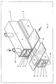
- Figur 1: einen Querschnitt durch die Einrichtung
- Figur 2: eine perspektivische Darstellung der Einrichtung
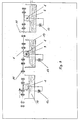
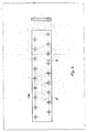
- Figur 3: eine schematische Darstellung der Verfahrensstufen Figur 4: eine Drauf- und eine Seitenansicht der Lochmaske.
- Hierein bedeuten:
- 1 Düsengehäuse
- 2 Vorkammer
- 3 Lochmaske
- 4 Düseninnenraum
- 5 Düse
- 6 Anode
- 7 Raum zwischen Düsengehäuse und Leiterplatte (8)
- 8 Leiterplatte
- 9 Ultraschallschwinger
- 10 Einlaufstutzen
- 11 Schleifkontakte
- 12 Behandlungslösung
- 13 Pumpe
- 14 Behälter
- 15 Führungsrollen
- A Einrichtung unterhalb der Leiterplattenebene
- A + B Einrichtung mit Ultraschallschwinger (9)
- A + C zwei Einrichtungen einander gegenüber senkrecht oder versetzt positioniert A + B + C zwei Einrichtungen einander gegenüber positioniert mit Ultraschallschwinger (9)
- A + D Einrichtung mit Elektrolyse (D) (Anode + Kathode)
- A + C + D zwei Einrichtungen gegenüber positioniert mit Elektrolyse (D) (Anode + Kathode)
- Die Arbeitsvorgänge laufen beim Betrieb im wesentlichen wie folgt ab:
- Durch mehrere Einlaufstutzen (10) wird die Behandlungslösung, wie zum Beispiel Wasser, in die Vorkammer (2) geleitet. Der Düseninnenraum ist durch eine Lochmaske (3) geteilt, durch die eine Verteilung der Strömung zur Düse erzielt wird. Der Düseninnenraum (4) vor der Schlitzdüse dient als Stauraum für eine gleichmäßige Ausbildung des Schwalls nach Passieren der Düse (5). Im Raum (7) zwischen dem Düsengehäuse (1) und der Leiterplatte (8) entsteht ein Überdruck, der die Lösung auch über den Bereich der hohen Strömung hin durch die Bohrlöcher zwingt. Im Fall der chemischen Behandlung der Leiterplatten wird nur mit der unteren Schwalldüse gearbeitet. Bei Reinigungsprozessen mit Uftraschall und elektrochemischen Prozessen wird mit zwei Schwalldüsen, die jeweils versetzt auf der Ober- und Unterseite der Leiterplatte positioniert sind, gearbeitet. In diesen Fällen ist in der Schwalldüse beziehungsweise oberhalb der Leiterplatte ein Ultraschallschwinger (9) installiert. Für die Elektrolyse ist eine Anode (6) im Innenraum fixiert. Die negative Polarisation der Leiterplatte (8) erfolgt über Schleifkontakte (11), die außerhalb des Naßbereichs vor und nach den Düsen positioniert sind.
- Das erfindungsgemäße Verfahren eignet sich insbesondere für die Behandlung von Leiterplatten für gedruckte Schaltungen, die in der Elektrotechnik Verwendung finden.
Claims (8)
Applications Claiming Priority (2)
| Application Number | Priority Date | Filing Date | Title |
|---|---|---|---|
| DE19853528575 DE3528575A1 (de) | 1985-08-06 | 1985-08-06 | Verfahren und einrichtung zur reinigung, aktivierung und/oder metallisierung von bohrloechern in horizontal gefuehrten leiterplatten |
| DE3528575 | 1985-08-06 |
Publications (4)
| Publication Number | Publication Date |
|---|---|
| EP0212253A2 EP0212253A2 (de) | 1987-03-04 |
| EP0212253A3 EP0212253A3 (en) | 1987-08-12 |
| EP0212253B1 true EP0212253B1 (de) | 1990-02-28 |
| EP0212253B2 EP0212253B2 (de) | 1998-11-11 |
Family
ID=6278093
Family Applications (1)
| Application Number | Title | Priority Date | Filing Date |
|---|---|---|---|
| EP86109731A Expired - Lifetime EP0212253B2 (de) | 1985-08-06 | 1986-07-16 | Verfahren und Einrichtung zur Reinigung, Aktivierung und/oder Metallisierung von Bohrlöchern in horizontal geführten Leiterplatten |
Country Status (11)
| Country | Link |
|---|---|
| US (1) | US4789405A (de) |
| EP (1) | EP0212253B2 (de) |
| JP (1) | JPS6297396A (de) |
| KR (1) | KR930010062B1 (de) |
| CN (1) | CN1016483B (de) |
| AT (1) | AT397011B (de) |
| BG (1) | BG49390A3 (de) |
| CA (1) | CA1276528C (de) |
| CZ (1) | CZ278956B6 (de) |
| DE (2) | DE3528575A1 (de) |
| SK (1) | SK278074B6 (de) |
Cited By (9)
| Publication number | Priority date | Publication date | Assignee | Title |
|---|---|---|---|---|
| EP0348752A1 (de) * | 1988-06-29 | 1990-01-03 | Schering Aktiengesellschaft | Vorrichtung und Verfahren zur Reinigung und Behandlung von horizontal bewegten Leiterplatten |
| EP0456870A1 (de) * | 1989-05-23 | 1991-11-21 | Schering Aktiengesellschaft | Anordnung zur chemischen Behandlung und/oder Reinigung von Gut, insbesondere von mit Bohrungen versehenen Leiterplatten, sowie dazugehöriges Verfahren (Fall B) |
| WO1992010923A1 (de) * | 1990-12-13 | 1992-06-25 | Schering Aktiengesellschaft | Verfahren zum durchfluten von bohrungen bei plattenförmigen werkstücken, und die vorrichtung zur durchführung des verfahrens |
| EP0421262A3 (en) * | 1989-09-30 | 1992-07-15 | Schering Aktiengesellschaft Berlin Und Bergkamen | Method of treating objects with a fluid and apparatus for realising this method |
| EP0329807B1 (de) * | 1988-02-25 | 1993-03-31 | Gebr. Schmid GmbH & Co. | Vorrichtung zur Behandlung von elektrischen Leiterplatten |
| WO1993010653A1 (en) * | 1991-11-12 | 1993-05-27 | Occleppo Di Francesco Occleppo & C. Snc | Device for formation of a film on the walls of holes in printed circuit boards |
| US5417828A (en) * | 1992-11-23 | 1995-05-23 | Sergio; Sala | Electroplating plant with opposed electrolitic cells and continuous feed of the workpieces to be plated |
| US6077359A (en) * | 1995-07-05 | 2000-06-20 | Atotech Deutschland Gmbh | Procedure and device for the chemical and electrolytic treatment of printed circuit boards and conductor films |
| DE10015349A1 (de) * | 2000-03-23 | 2001-10-25 | Atotech Deutschland Gmbh | Verfahren und Vorrichtung zum Behandeln von durchgehende Löcher und/oder Vertiefungen aufweisenden Schaltungsträgern sowie Anwendung des Verfahrens und Verwendung der Vorrichtung |
Families Citing this family (26)
| Publication number | Priority date | Publication date | Assignee | Title |
|---|---|---|---|---|
| DE3638630A1 (de) * | 1986-11-11 | 1988-05-26 | Schering Ag | Verfahren zur entfernung von harzverschmutzungen in bohrloechern von leiterplatten |
| DE8703114U1 (de) * | 1987-02-25 | 1987-04-09 | Schering AG, 1000 Berlin und 4709 Bergkamen | Einrichtung zur Reinigung oder chemischen Behandlung von Werkstücken |
| DE3916693A1 (de) * | 1989-05-23 | 1990-11-29 | Schering Ag | Anordnung zur behandlung und/oder reinigung von gut, insbesondere von mit bohrungen versehenen leiterplatten |
| DE3935831A1 (de) * | 1989-10-27 | 1991-05-02 | Hoellmueller Maschbau H | Anlage zur herstellung von durchkontaktierten leiterplatten und multilayern |
| US5289639A (en) * | 1992-07-10 | 1994-03-01 | International Business Machines Corp. | Fluid treatment apparatus and method |
| US5378307A (en) * | 1993-04-28 | 1995-01-03 | International Business Machines Corporation | Fluid treatment apparatus |
| DE4402596C2 (de) * | 1994-01-28 | 1997-03-27 | Atotech Deutschland Gmbh | Elektrolytisches Verfahren in horizontalen Durchlaufanlagen und Vorrichtung zur Durchführung desselben |
| WO1996021341A1 (de) * | 1995-01-05 | 1996-07-11 | Hübel, Egon | Verfahren und vorrichtung zur behandlung von mit feinsten löchern versehenen plattenförmigen werkstücken |
| US5720813A (en) | 1995-06-07 | 1998-02-24 | Eamon P. McDonald | Thin sheet handling system |
| US5741361A (en) * | 1995-07-06 | 1998-04-21 | Allan H. McKinnon | Method for fluid transport |
| US5904773A (en) | 1995-08-11 | 1999-05-18 | Atotech Usa, Inc. | Fluid delivery apparatus |
| US5614264A (en) | 1995-08-11 | 1997-03-25 | Atotech Usa, Inc. | Fluid delivery apparatus and method |
| DE19530989C1 (de) * | 1995-08-23 | 1997-03-13 | Atotech Deutschland Gmbh | Verfahren zum Filmstrippen |
| DE19534521C1 (de) * | 1995-09-06 | 1996-11-21 | Atotech Deutschland Gmbh | Verfahren und Vorrichtung zum Behandeln von sich in Werkstücke erstreckende Löcher oder Vertiefungen mit flüssigen Behandlungsmitteln und Anwendung des Verfahrens zur Behandlung von Leiterplatten |
| JP3005898B2 (ja) * | 1998-04-30 | 2000-02-07 | 東京化工機株式会社 | 液体噴射装置 |
| US6336976B1 (en) * | 1999-01-04 | 2002-01-08 | Kabushiki Kaisha Sankyo Seiki Seisakusho | Hole processing apparatus and method thereof and dynamic pressure bearings cleaning method |
| JP3120073B2 (ja) * | 1999-02-22 | 2000-12-25 | 東京化工機株式会社 | 薬液処理装置 |
| DE10110823A1 (de) * | 2001-03-07 | 2002-10-02 | Bosch Gmbh Robert | Verfahren zum Abtragen von Materialablagerungen, die bei einer Laserbearbeitung entstehen |
| DE10255884B4 (de) * | 2002-11-29 | 2006-05-11 | Atotech Deutschland Gmbh | Düsenanordnung |
| DE10323658A1 (de) * | 2003-05-15 | 2004-12-02 | Gebr. Schmid Gmbh & Co. | Verfahren und Vorrichtung zur Beschichtung eines Substrats |
| DE102004002421A1 (de) * | 2004-01-16 | 2005-08-18 | Atotech Deutschland Gmbh | Düsenanordnung |
| GB2459055B (en) * | 2007-01-11 | 2012-05-23 | Peter Philip Andrew Lymn | Liquid treatment apparatus |
| CN102950127A (zh) * | 2012-11-12 | 2013-03-06 | 大连太平洋电子有限公司 | 一种线路板钻孔刀具的清洗方法 |
| JP6160147B2 (ja) * | 2013-03-19 | 2017-07-12 | Tdk株式会社 | 電子部品モジュールの製造方法、無電解メッキ方法及び無電解メッキ装置 |
| CN115707197B (zh) * | 2021-08-16 | 2026-06-26 | 昆山东威科技股份有限公司 | 一种电路板活化设备及电路板生产线 |
| CN120287016A (zh) * | 2025-04-01 | 2025-07-11 | 深圳市中联讯科技有限公司 | 一种用于手机电池盖模具的表面处理方法 |
Family Cites Families (13)
| Publication number | Priority date | Publication date | Assignee | Title |
|---|---|---|---|---|
| US3868272A (en) * | 1973-03-05 | 1975-02-25 | Electrovert Mfg Co Ltd | Cleaning of printed circuit boards by solid and coherent jets of cleaning liquid |
| FR2301307A1 (fr) * | 1975-02-24 | 1976-09-17 | Applic Meca Pour Ind Labo | Installation pour le traitement de produits par passage dans un liquide |
| DE2606984C3 (de) * | 1976-02-20 | 1978-08-24 | Siemens Ag | Verfahren und Einrichtung zum chemischen Reinigen von Kontaktierungslöchern in Leiterplatten |
| DE2724091A1 (de) * | 1976-05-28 | 1977-12-15 | Sumitomo Chemical Co | Verfahren zum reinigen und/oder tauchbeschichten von kunstharzgegenstaenden und vorrichtung zur durchfuehrung des verfahrens |
| US4076222A (en) * | 1976-07-19 | 1978-02-28 | Schaming Edward J | Runout cooling method and apparatus for metal rolling mills |
| US4132567A (en) * | 1977-10-13 | 1979-01-02 | Fsi Corporation | Apparatus for and method of cleaning and removing static charges from substrates |
| JPS5621147A (en) * | 1979-07-27 | 1981-02-27 | Xerox Corp | Sheet collector and sorter |
| DE3006045A1 (de) * | 1980-02-18 | 1981-08-20 | Siemens AG, 1000 Berlin und 8000 München | Verfahren und vorrichtung zur behandlung, insbesondere reinigung, von flachen objekten |
| DE3011061C2 (de) * | 1980-03-21 | 1983-12-22 | Siemens AG, 1000 Berlin und 8000 München | Verfahren zur Intensivierung von Spül- und Reinigungsprozessen für Perforationen in Formstücken in Spül- und Reinigungsautomaten |
| JPS5858292A (ja) * | 1981-09-30 | 1983-04-06 | Electroplating Eng Of Japan Co | 微小孔を有するメツキ物のメツキ装置 |
| DE3305564C1 (de) * | 1983-02-15 | 1984-03-22 | Siemens AG, 1000 Berlin und 8000 München | Verfahren zum Aufbau von metallisierten Leiterbahnen und Durchkontaktierungen an gelochten Leiterplatten |
| SE440719B (sv) * | 1983-06-17 | 1985-08-12 | Holmstrands Plaatindustri Ab | Sett och anordning vid rengoring av kretskort, som tidigare underkastats en lodningsoperation med flussmedel |
| US4543130A (en) * | 1984-08-28 | 1985-09-24 | Rca Corporation | Megasonic cleaning apparatus and method |
-
1985
- 1985-08-06 DE DE19853528575 patent/DE3528575A1/de not_active Ceased
-
1986
- 1986-07-16 EP EP86109731A patent/EP0212253B2/de not_active Expired - Lifetime
- 1986-07-16 DE DE8686109731T patent/DE3669256D1/de not_active Expired - Lifetime
- 1986-08-01 BG BG076053A patent/BG49390A3/xx unknown
- 1986-08-04 AT AT0209586A patent/AT397011B/de not_active IP Right Cessation
- 1986-08-04 US US06/893,563 patent/US4789405A/en not_active Expired - Lifetime
- 1986-08-05 CN CN86105385A patent/CN1016483B/zh not_active Expired
- 1986-08-06 CZ CS865884A patent/CZ278956B6/cs not_active IP Right Cessation
- 1986-08-06 SK SK5884-86A patent/SK278074B6/sk unknown
- 1986-08-06 CA CA000515424A patent/CA1276528C/en not_active Expired - Lifetime
- 1986-08-06 JP JP61183566A patent/JPS6297396A/ja active Granted
- 1986-08-06 KR KR1019860006487A patent/KR930010062B1/ko not_active Expired - Fee Related
Cited By (10)
| Publication number | Priority date | Publication date | Assignee | Title |
|---|---|---|---|---|
| EP0329807B1 (de) * | 1988-02-25 | 1993-03-31 | Gebr. Schmid GmbH & Co. | Vorrichtung zur Behandlung von elektrischen Leiterplatten |
| EP0348752A1 (de) * | 1988-06-29 | 1990-01-03 | Schering Aktiengesellschaft | Vorrichtung und Verfahren zur Reinigung und Behandlung von horizontal bewegten Leiterplatten |
| EP0456870A1 (de) * | 1989-05-23 | 1991-11-21 | Schering Aktiengesellschaft | Anordnung zur chemischen Behandlung und/oder Reinigung von Gut, insbesondere von mit Bohrungen versehenen Leiterplatten, sowie dazugehöriges Verfahren (Fall B) |
| EP0421262A3 (en) * | 1989-09-30 | 1992-07-15 | Schering Aktiengesellschaft Berlin Und Bergkamen | Method of treating objects with a fluid and apparatus for realising this method |
| WO1992010923A1 (de) * | 1990-12-13 | 1992-06-25 | Schering Aktiengesellschaft | Verfahren zum durchfluten von bohrungen bei plattenförmigen werkstücken, und die vorrichtung zur durchführung des verfahrens |
| WO1993010653A1 (en) * | 1991-11-12 | 1993-05-27 | Occleppo Di Francesco Occleppo & C. Snc | Device for formation of a film on the walls of holes in printed circuit boards |
| US5417828A (en) * | 1992-11-23 | 1995-05-23 | Sergio; Sala | Electroplating plant with opposed electrolitic cells and continuous feed of the workpieces to be plated |
| US6077359A (en) * | 1995-07-05 | 2000-06-20 | Atotech Deutschland Gmbh | Procedure and device for the chemical and electrolytic treatment of printed circuit boards and conductor films |
| DE10015349A1 (de) * | 2000-03-23 | 2001-10-25 | Atotech Deutschland Gmbh | Verfahren und Vorrichtung zum Behandeln von durchgehende Löcher und/oder Vertiefungen aufweisenden Schaltungsträgern sowie Anwendung des Verfahrens und Verwendung der Vorrichtung |
| US6908515B2 (en) | 2000-03-23 | 2005-06-21 | Atotech Deutschland Gmbh | Treatment of circuit support with impulse excitation |
Also Published As
| Publication number | Publication date |
|---|---|
| JPH0445996B2 (de) | 1992-07-28 |
| CN86105385A (zh) | 1987-04-01 |
| BG49390A3 (en) | 1991-10-15 |
| CN1016483B (zh) | 1992-04-29 |
| SK278074B6 (en) | 1995-12-06 |
| CA1276528C (en) | 1990-11-20 |
| CZ278956B6 (en) | 1994-10-19 |
| US4789405A (en) | 1988-12-06 |
| AT397011B (de) | 1994-01-25 |
| EP0212253A2 (de) | 1987-03-04 |
| DE3669256D1 (de) | 1990-04-05 |
| JPS6297396A (ja) | 1987-05-06 |
| EP0212253B2 (de) | 1998-11-11 |
| ATA209586A (de) | 1993-05-15 |
| KR870002752A (ko) | 1987-04-06 |
| EP0212253A3 (en) | 1987-08-12 |
| KR930010062B1 (ko) | 1993-10-14 |
| DE3528575A1 (de) | 1987-02-19 |
Similar Documents
| Publication | Publication Date | Title |
|---|---|---|
| EP0212253B2 (de) | Verfahren und Einrichtung zur Reinigung, Aktivierung und/oder Metallisierung von Bohrlöchern in horizontal geführten Leiterplatten | |
| DE69317703T2 (de) | Vorrichtung und Verfahren zur Behandlung mit Flüssigkeit | |
| DE69328328T2 (de) | Verfahren und Gerät zur Flüssigbehandlung | |
| DE69414324T2 (de) | Elektrobeschichtungsverfahren | |
| AT395721B (de) | Einrichtung zur reinigung oder chemischen behandlung von werkstuecken | |
| DE19740431C1 (de) | Verfahren zum Metallisieren eines elektrisch nichtleitende Oberflächenbereiche aufweisenden Substrats | |
| DE69602398T2 (de) | Verfahren zum Flüssigkeitstransport | |
| DE69009978T3 (de) | Verfahren zum stromlosen Abscheiden von Kupfer. | |
| DE69316750T2 (de) | Verfahren zur herstellung einer leiterplatte. | |
| EP0152600B1 (de) | Vorrichtung und Verfahren zur Behandlung von Leiterplatten | |
| EP0267452B1 (de) | Verfahren zur Entfernung von Harzverschmutzungen in Bohrlöchern von Leiterplatten | |
| EP1165861A1 (de) | Kupfergewinnungsverfahren | |
| EP0348752B1 (de) | Vorrichtung und Verfahren zur Reinigung und Behandlung von horizontal bewegten Leiterplatten | |
| EP0329807B1 (de) | Vorrichtung zur Behandlung von elektrischen Leiterplatten | |
| DE69012454T2 (de) | Verfahren mit abgekürztem Zyklus zur Herstellung von gedruckten Leiterplatten und Zusammensetzung für die Anwendung. | |
| EP0381082B1 (de) | Verfahren zum Lackieren einer Baugruppe in einem Gehäuse | |
| DE9011675U1 (de) | Vorrichtung zur Oberflächenbehandlung und Galvanisierung von plattenförmigem Material | |
| DE69220575T2 (de) | Gestell für Vorrichtungen zur Oberflächenbehandlung mit Bädern sowie Herstellungsverfahren | |
| DE2455363A1 (de) | Verfahren zur herstellung duenner schichten aus halbleitermaterial | |
| DE3041551A1 (de) | Elektroden fuer plasma-aetzanlage | |
| DE19715368C2 (de) | Verfahren und Vorrichtung zur Herstellung einer Multi-Layer-Leiterplatte | |
| DE4040226A1 (de) | Verfahren zur herstellung von durchkontaktierten leiterplatten oder multilayern | |
| DE19723682A1 (de) | Verfahren zur Reinigung und Beize von Oberflächen mit Regeneration des Reinigungs- und Beizmittels | |
| DE2807593A1 (de) | Strahl-elektrolysevorrichtung | |
| DE3927440A1 (de) | Verfahren zur direkten metallisierung eines nicht leitenden substrats |
Legal Events
| Date | Code | Title | Description |
|---|---|---|---|
| PUAI | Public reference made under article 153(3) epc to a published international application that has entered the european phase |
Free format text: ORIGINAL CODE: 0009012 |
|
| 17P | Request for examination filed |
Effective date: 19860716 |
|
| AK | Designated contracting states |
Kind code of ref document: A2 Designated state(s): BE CH DE FR GB IT LI LU NL SE |
|
| PUAL | Search report despatched |
Free format text: ORIGINAL CODE: 0009013 |
|
| AK | Designated contracting states |
Kind code of ref document: A3 Designated state(s): BE CH DE FR GB IT LI LU NL SE |
|
| 17Q | First examination report despatched |
Effective date: 19880408 |
|
| GRAA | (expected) grant |
Free format text: ORIGINAL CODE: 0009210 |
|
| ITF | It: translation for a ep patent filed | ||
| AK | Designated contracting states |
Kind code of ref document: B1 Designated state(s): BE CH DE FR GB IT LI LU NL SE |
|
| REF | Corresponds to: |
Ref document number: 3669256 Country of ref document: DE Date of ref document: 19900405 |
|
| GBT | Gb: translation of ep patent filed (gb section 77(6)(a)/1977) | ||
| ET | Fr: translation filed | ||
| PLBI | Opposition filed |
Free format text: ORIGINAL CODE: 0009260 |
|
| 26 | Opposition filed |
Opponent name: SHIPLEY COMPANY INC. Effective date: 19901128 Opponent name: GEBR. SCHMID GMBH & CO. Effective date: 19901127 |
|
| NLR1 | Nl: opposition has been filed with the epo |
Opponent name: SHIPLEY COMPANY INC. Opponent name: GEBR. SCHMID GMBH & CO. |
|
| PLAB | Opposition data, opponent's data or that of the opponent's representative modified |
Free format text: ORIGINAL CODE: 0009299OPPO |
|
| R26 | Opposition filed (corrected) |
Opponent name: GEBR. SCHMID GMBH & CO. * 901128 SHIPLEY COMPANY I Effective date: 19901127 |
|
| PLAB | Opposition data, opponent's data or that of the opponent's representative modified |
Free format text: ORIGINAL CODE: 0009299OPPO |
|
| PLAB | Opposition data, opponent's data or that of the opponent's representative modified |
Free format text: ORIGINAL CODE: 0009299OPPO |
|
| R26 | Opposition filed (corrected) |
Opponent name: GEBR. SCHMID GMBH & CO. * 901128 SHIPLEY COMPANY I Effective date: 19901127 |
|
| R26 | Opposition filed (corrected) |
Opponent name: GEBR. SCHMID GMBH & CO. * 901128 SHIPLEY COMPANY I Effective date: 19901127 |
|
| PGFP | Annual fee paid to national office [announced via postgrant information from national office to epo] |
Ref country code: LU Payment date: 19930701 Year of fee payment: 8 |
|
| ITTA | It: last paid annual fee | ||
| EPTA | Lu: last paid annual fee | ||
| PG25 | Lapsed in a contracting state [announced via postgrant information from national office to epo] |
Ref country code: LU Free format text: LAPSE BECAUSE OF NON-PAYMENT OF DUE FEES Effective date: 19940716 |
|
| EAL | Se: european patent in force in sweden |
Ref document number: 86109731.9 |
|
| REG | Reference to a national code |
Ref country code: CH Ref legal event code: PUE Owner name: SCHERING AKTIENGESELLSCHAFT, BERLIN & BERGKAMEN -D |
|
| RAP2 | Party data changed (patent owner data changed or rights of a patent transferred) |
Owner name: ATOTECH DEUTSCHLAND GMBH |
|
| APAC | Appeal dossier modified |
Free format text: ORIGINAL CODE: EPIDOS NOAPO |
|
| NLT2 | Nl: modifications (of names), taken from the european patent patent bulletin |
Owner name: ATOTECH DEUTSCHLAND GMBH |
|
| REG | Reference to a national code |
Ref country code: FR Ref legal event code: TP |
|
| REG | Reference to a national code |
Ref country code: GB Ref legal event code: 732E |
|
| NLS | Nl: assignments of ep-patents |
Owner name: ATOTECH DEUTSCHLAND GMBH |
|
| PLAW | Interlocutory decision in opposition |
Free format text: ORIGINAL CODE: EPIDOS IDOP |
|
| PLAW | Interlocutory decision in opposition |
Free format text: ORIGINAL CODE: EPIDOS IDOP |
|
| PUAH | Patent maintained in amended form |
Free format text: ORIGINAL CODE: 0009272 |
|
| STAA | Information on the status of an ep patent application or granted ep patent |
Free format text: STATUS: PATENT MAINTAINED AS AMENDED |
|
| 27A | Patent maintained in amended form |
Effective date: 19981111 |
|
| AK | Designated contracting states |
Kind code of ref document: B2 Designated state(s): BE CH DE FR GB IT LI LU NL SE |
|
| REG | Reference to a national code |
Ref country code: CH Ref legal event code: AEN Free format text: AUFRECHTERHALTUNG DES PATENTES IN GEAENDERTER FORM |
|
| NLR2 | Nl: decision of opposition | ||
| ITF | It: translation for a ep patent filed | ||
| GBTA | Gb: translation of amended ep patent filed (gb section 77(6)(b)/1977) | ||
| ET3 | Fr: translation filed ** decision concerning opposition | ||
| NLR3 | Nl: receipt of modified translations in the netherlands language after an opposition procedure | ||
| REG | Reference to a national code |
Ref country code: GB Ref legal event code: IF02 |
|
| PGFP | Annual fee paid to national office [announced via postgrant information from national office to epo] |
Ref country code: FR Payment date: 20040610 Year of fee payment: 19 |
|
| PGFP | Annual fee paid to national office [announced via postgrant information from national office to epo] |
Ref country code: CH Payment date: 20040611 Year of fee payment: 19 |
|
| PGFP | Annual fee paid to national office [announced via postgrant information from national office to epo] |
Ref country code: NL Payment date: 20040614 Year of fee payment: 19 Ref country code: GB Payment date: 20040614 Year of fee payment: 19 |
|
| PGFP | Annual fee paid to national office [announced via postgrant information from national office to epo] |
Ref country code: SE Payment date: 20040616 Year of fee payment: 19 |
|
| PGFP | Annual fee paid to national office [announced via postgrant information from national office to epo] |
Ref country code: DE Payment date: 20040621 Year of fee payment: 19 |
|
| PGFP | Annual fee paid to national office [announced via postgrant information from national office to epo] |
Ref country code: BE Payment date: 20040713 Year of fee payment: 19 |
|
| PG25 | Lapsed in a contracting state [announced via postgrant information from national office to epo] |
Ref country code: IT Free format text: LAPSE BECAUSE OF NON-PAYMENT OF DUE FEES;WARNING: LAPSES OF ITALIAN PATENTS WITH EFFECTIVE DATE BEFORE 2007 MAY HAVE OCCURRED AT ANY TIME BEFORE 2007. THE CORRECT EFFECTIVE DATE MAY BE DIFFERENT FROM THE ONE RECORDED. Effective date: 20050716 Ref country code: GB Free format text: LAPSE BECAUSE OF NON-PAYMENT OF DUE FEES Effective date: 20050716 |
|
| PG25 | Lapsed in a contracting state [announced via postgrant information from national office to epo] |
Ref country code: SE Free format text: LAPSE BECAUSE OF NON-PAYMENT OF DUE FEES Effective date: 20050717 |
|
| PG25 | Lapsed in a contracting state [announced via postgrant information from national office to epo] |
Ref country code: LI Free format text: LAPSE BECAUSE OF NON-PAYMENT OF DUE FEES Effective date: 20050731 Ref country code: CH Free format text: LAPSE BECAUSE OF NON-PAYMENT OF DUE FEES Effective date: 20050731 Ref country code: BE Free format text: LAPSE BECAUSE OF NON-PAYMENT OF DUE FEES Effective date: 20050731 |
|
| APAH | Appeal reference modified |
Free format text: ORIGINAL CODE: EPIDOSCREFNO |
|
| PG25 | Lapsed in a contracting state [announced via postgrant information from national office to epo] |
Ref country code: NL Free format text: LAPSE BECAUSE OF NON-PAYMENT OF DUE FEES Effective date: 20060201 Ref country code: DE Free format text: LAPSE BECAUSE OF NON-PAYMENT OF DUE FEES Effective date: 20060201 |
|
| REG | Reference to a national code |
Ref country code: CH Ref legal event code: PL |
|
| EUG | Se: european patent has lapsed | ||
| GBPC | Gb: european patent ceased through non-payment of renewal fee |
Effective date: 20050716 |
|
| PG25 | Lapsed in a contracting state [announced via postgrant information from national office to epo] |
Ref country code: FR Free format text: LAPSE BECAUSE OF NON-PAYMENT OF DUE FEES Effective date: 20060331 |
|
| NLV4 | Nl: lapsed or anulled due to non-payment of the annual fee |
Effective date: 20060201 |
|
| REG | Reference to a national code |
Ref country code: FR Ref legal event code: ST Effective date: 20060331 |
|
| BERE | Be: lapsed |
Owner name: *ATOTECH DEUTSCHLAND G.M.B.H. Effective date: 20050731 |