EP0213453B1 - Verminderung des Rauschens während des Prüfens von integrierten Schaltungschips - Google Patents
Verminderung des Rauschens während des Prüfens von integrierten Schaltungschips Download PDFInfo
- Publication number
- EP0213453B1 EP0213453B1 EP86110981A EP86110981A EP0213453B1 EP 0213453 B1 EP0213453 B1 EP 0213453B1 EP 86110981 A EP86110981 A EP 86110981A EP 86110981 A EP86110981 A EP 86110981A EP 0213453 B1 EP0213453 B1 EP 0213453B1
- Authority
- EP
- European Patent Office
- Prior art keywords
- input
- driver
- chip
- tester
- output
- Prior art date
- Legal status (The legal status is an assumption and is not a legal conclusion. Google has not performed a legal analysis and makes no representation as to the accuracy of the status listed.)
- Expired - Lifetime
Links
- 238000012360 testing method Methods 0.000 title claims abstract description 90
- 230000009467 reduction Effects 0.000 title description 2
- 238000012163 sequencing technique Methods 0.000 claims abstract description 37
- 238000000034 method Methods 0.000 claims description 15
- 238000000926 separation method Methods 0.000 claims description 5
- 230000004044 response Effects 0.000 claims description 3
- 238000010998 test method Methods 0.000 claims description 2
- 230000001143 conditioned effect Effects 0.000 claims 1
- 230000008859 change Effects 0.000 description 9
- 238000013461 design Methods 0.000 description 5
- 230000008878 coupling Effects 0.000 description 4
- 238000010168 coupling process Methods 0.000 description 4
- 238000005859 coupling reaction Methods 0.000 description 4
- 238000010586 diagram Methods 0.000 description 4
- 238000004806 packaging method and process Methods 0.000 description 4
- 239000003990 capacitor Substances 0.000 description 3
- 230000009471 action Effects 0.000 description 2
- 230000002401 inhibitory effect Effects 0.000 description 2
- 230000002265 prevention Effects 0.000 description 2
- 238000000638 solvent extraction Methods 0.000 description 2
- 238000003491 array Methods 0.000 description 1
- 238000011990 functional testing Methods 0.000 description 1
- 238000010348 incorporation Methods 0.000 description 1
- 230000010354 integration Effects 0.000 description 1
- 239000011159 matrix material Substances 0.000 description 1
- 238000005259 measurement Methods 0.000 description 1
- 230000010355 oscillation Effects 0.000 description 1
- 239000000523 sample Substances 0.000 description 1
- 239000004065 semiconductor Substances 0.000 description 1
- 238000004088 simulation Methods 0.000 description 1
Images


Classifications
-
- G—PHYSICS
- G01—MEASURING; TESTING
- G01R—MEASURING ELECTRIC VARIABLES; MEASURING MAGNETIC VARIABLES
- G01R31/00—Arrangements for testing electric properties; Arrangements for locating electric faults; Arrangements for electrical testing characterised by what is being tested not provided for elsewhere
- G01R31/28—Testing of electronic circuits, e.g. by signal tracer
- G01R31/316—Testing of analog circuits
-
- G—PHYSICS
- G01—MEASURING; TESTING
- G01R—MEASURING ELECTRIC VARIABLES; MEASURING MAGNETIC VARIABLES
- G01R31/00—Arrangements for testing electric properties; Arrangements for locating electric faults; Arrangements for electrical testing characterised by what is being tested not provided for elsewhere
- G01R31/28—Testing of electronic circuits, e.g. by signal tracer
- G01R31/317—Testing of digital circuits
- G01R31/3181—Functional testing
- G01R31/319—Tester hardware, i.e. output processing circuits
- G01R31/31917—Stimuli generation or application of test patterns to the device under test [DUT]
- G01R31/31924—Voltage or current aspects, e.g. driver, receiver
-
- G—PHYSICS
- G01—MEASURING; TESTING
- G01R—MEASURING ELECTRIC VARIABLES; MEASURING MAGNETIC VARIABLES
- G01R31/00—Arrangements for testing electric properties; Arrangements for locating electric faults; Arrangements for electrical testing characterised by what is being tested not provided for elsewhere
- G01R31/28—Testing of electronic circuits, e.g. by signal tracer
- G01R31/317—Testing of digital circuits
- G01R31/3181—Functional testing
- G01R31/319—Tester hardware, i.e. output processing circuits
- G01R31/3193—Tester hardware, i.e. output processing circuits with comparison between actual response and known fault free response
Definitions
- EP-A-132,522 published February 13, 1985, entitled “Oscillation Prevention During Testing of Integrated Circuit Logic Chips”.
- This invention relates to testing of integrated circuit logic chips and more particularly to excessive noise (Delta I) prevention during the testing thereof.
- delta I When many off chip drivers switch simultaneously a large change in power supply current results (delta I).
- This delta I current path flows from the driver output wire, through the driver, through the unbypassed inductance and resistance of the power supply distribution network, through the bypass capacitor and back to the tester ground.
- dI and dI/dt relate directly to the driver type and the number of drivers concurrently switching, as does the noise magnitude.
- Voltage and current signals which change as a driver changes state also couple through mutual inductance and mutual capacitance into nearby I/O paths.
- Mutual inductance and mutual capacitance coupling may contribute, or solely result in false switching and test failures.
- the noise magnitude relates directly to the driver type (speed) and the number of drivers coupling noise into a nearby I/O path.
- the method prevents off-chip drivers from switching during parametric testing and hence the occurrence of delta I noise which could affect the results of the test. It, however, has the disadvantage that all of the drivers are inhibited at the same time and it is not possible to inhibit only a few drivers whilst allowing others to change logical value. It also suffers from the further disadvantage that, switching off the off-chip driver inhibit network can in itself cause delta I problems due to the large number of drivers that may change state at the same time. It should be noted that the word 'sequence' as used in this prior art document carries a different meaning from the 'sequential testing' used in the description of the current invention below.
- the aforementioned article by BANKER et al, "Driver-Sequencing Circuit", in the IBM Technical Disclosure Bulletin, vol 26, no 7B, December 1983, pp 3621-3622 discloses a driver sequencing circuit (DSC) which greatly reduces the noise caused by all the drivers switching at the same time.
- DSC driver sequencing circuit
- a circuit is described whose output triggers a further circuit; thus the driver sequencing circuits can be cascaded to sequentially turn on individual groups of off-chip drivers.
- the delay time between one group of drivers switching on and the next group of drivers being turned on is set by the size of one of the transistors and is typically 100ns. Its value cannot be varied by the tester to take into account the different characteristics of the logic device under test.
- the invention may be summarized as a driver sequencing network (DSN) on the integrated circuit device, or chip, to be tested which gives the tester (machine) control of the timing between the switching of groups of driver circuits so that more than a predetermined number of driver circuits concurrently switching state is precluded.
- the driver sequencing network is such that no one group of driver output pins can create enough delta I or coupled noise to cause a test failure.
- the driver sequencing network may be disabled to give full control of the driver outputs to the device being tested. In a normal application, i.e. the intended purpose or function of the device, the driver sequencing network is disabled.
- the function of the driver sequencing network is to control off chip driver switching during test. (An "off chip driver” is an output amplifier contained on the chip, to generate device output signals, also called off chip signals.)
- the 'sequence' referred to in respect to the current invention does not describe the order in which test patterns are applied to the integrated circuit device, or chip, under test, but to the act of switching the driver circuits one after another.
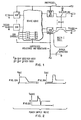
- FIG. 1 illustrates, in accordance with the prior art, the delta I current path from the driver output wire, through the driver, through the unbypassed inductance and resistance of the power supply distribution network, through the bypass capacitor and back to the tester ground; the incorporation of a DSN according to the invention is also illustrated.
- FIG. 2 is comprised of FIGS. 2A, 2B and 2C.
- FIG. 2A depicts a voltage waveform imposed on the driver output wire by an off chip driver during switching.
- FIG. 2B depicts a delta I waveform which occurs on the delta I path shown in the circuitry of FIG. 1.
- FIG. 2C depicts the voltage generated across the unbypassed inductance and resistance of the prior art circuitry of FIG. 1.
- FIG. 3 is comprised of FIGS. 3A, 3B and 3C.
- FIG. 3C depicts the combined voltage noise waveform at the output of the prior art circuitry of FIG. 1.
- FIG. 4 shows a representative driver sequencing network in accordance with the invention.
- FIG. 5 shows a preferred embodiment of the invention wherein an integrated circuit chip under test includes a driver sequence network (DSN).
- DSN driver sequence network
- FIG. 7 shows a block diagram of the driver circuit of FIG. 6.
- FIG. 8 shows a timing diagram to be reviewed in conjunction with the explanation of operation of the invention as illustrated in FIG. 5 .
- FIG. 4 shows an example of a driver sequencing network. Inputs labeled “+ Inhibit,” “Shift In,” “L1 Clock,” and “L2 Clock” are controlled by the tester. Outputs “+ Inhibit Group 1" through “+ Inhibit Group 4" continue on the chip as the inhibit control lines for the respective off chip driver groups.
- the driver sequencing network shown is on the chip.
- DSN driver sequencing network
- All of the items listed above are fabricated on the chip and, except for the said driver inhibit inputs, are normal or conventional to a VLSI chip.
- a Driver Sequence Network To embody a Driver Sequence Network, additional receivers, drivers and logic is required.
- a representative DSN is shown enclosed within a broken line bearing the legend "Driver Sequencing Network" at the lower right of FIG. 5.
- the off chip drivers D3 through D102 are divided into ten groups of ten drivers each. Each group shares a common inhibit line so that there are ten separate group inhibit lines, one for each driver group. Again, D2 does not get inhibited because it provides the shift register output function.
- the group inhibit lines may all be set to the inhibiting state simultaneously by the "+ Inhibit" control line or each group inhibit line may be brought up sequentially by using the 'Sequence Scan In', '+L1 Clock', and '+L2 Clock' to shift a logical '1' through the ten shift register latches (L1 through L10).
- the "+ Inhibit" line may allow all group inhibit lines to go to the enable state simultaneously, or each line may be enabled sequentially by shifting a logical '0' through the ten latches (See FIG. 8 for a timing diagram of the shift operation; the shifting of a logical '1' is shown).
- Driver DI facilitates testing of the sequencing shift register of the DSN by providing a shift register output to the tester.
- test execution steps can be used to prevent too many off chip drivers from switching simultaneously.
Landscapes
- Engineering & Computer Science (AREA)
- General Engineering & Computer Science (AREA)
- Physics & Mathematics (AREA)
- General Physics & Mathematics (AREA)
- Tests Of Electronic Circuits (AREA)
- Testing Or Measuring Of Semiconductors Or The Like (AREA)
- Semiconductor Integrated Circuits (AREA)
Claims (6)
- Prüfsystem mit Mitteln zum Vermindern der Störspannung beim Schalten der Treiber, wobei das Prüfsystem ein Prüfgerät zum elektrischen Prüfen eines Bauelements mit integrierter Schaltung verwendet und das Prüfgerät mit dem Bauelement mit integrierter Schaltung verbunden ist,
wobei das Bauelement mit integrierter Schaltung eine Vielzahl von Eingangsanschlüssen zum Empfangen eines elektrischen Prüfmusters von dem Prüfgerät aufweist, eine Vielzahl von Ausgangsanschlüssen zum Liefern eines Ausgangsmusters an das Prüfgerät, eine Folgeschaltung (L1-L20) für die Treiber und eine Vielzahl von Ausgangstreiberschaltungen (D3-D102), deren Ausgänge mit den Ausgangsanschlüssen des Bauelements mit integrierter Schaltung verbunden sind, wobei die Folgeschaltung (L1-L10) für die Treiber auf zumindest ein Steuersignal des Prüfgerätes anspricht,
und das Prüfsystem dadurch gekennzeichnet ist, daß die Folgeschaltung (L1-L10) für die Treiber aufeinanderfolgende der Ausgangstreiberschaltungen (D3-D102) aktiviert oder deaktiviert, wodurch die Vielzahl von Treibern sequentiell in Gruppen (D3-D102) aktiviert und deaktiviert werden, die eine oder mehrere Treiber enthalten, und die Zeitverzögerung zwischen dem Aktivieren oder Deaktivieren einer Gruppe von Treibern (D3-D102) und dem Aktivieren oder Deaktivieren einer nachfolgenden Gruppe von Treibern (D3-D102) veränderlich ist. - Prüfsystem nach Anspruch 1, bei dem das Bauelement mit integrierter Schaltung enthält
logische Schaltungsmittel, die zwischen der Vielzahl von Eingangsanschlüssen und einer Vielzahl von Treiberschaltungseingängen angeschlossen sind, wobei die logischen Schaltmittel ein binäres Eingangssignal empfangen und ein binäres Ausgangssignal an die Treiberschaltungen (D3-D102) liefern, das eine vorgegebene logische Funktion des binären Eingangssignals an der Vielzahl von Eingangsanschlüssen ist. - Prüfsystem nach Anspruch 1, bei dem
jede der Treiberschaltungen (D3-D102) eine chipexterne Treiberschaltung ist, die einen ersten Binärzustand, einen zweiten Binärzustand oder einen Zustand, in dem das Schalten verhindert ist, annehmen kann, wobei jede der chipexternen Treiberschaltungen zumindest einen logischen Eingang und einen Sperreingang aufweist,
und die Folgeschaltung (L1-L10) für die Treiber mit dem Sperreingang jeder der chipexternen Treiberschaltungen gekoppelt ist, wobei die Folgeschaltung (L1-L10) für die Treiber einen Sperreingang (R4) zusätzlich zu dem zumindest einen Eingang (R3) aufweist, wobei der Sperreingang (R4) der Folgeschaltung (L1-L10) für die Treiber mit dem Prüfgerät verbunden ist, wodurch als Antwort auf ein Sperrsignal des Prüfgerätes, das an den Sperreingang (R4) der Folgeschaltung (L1-L10) für die Treiber angelegt wird, jede der chipexternen Treiberschaltungen den Sperrzustand annimmt. - Prüfsystem nach Anspruch 3, bei dem die Vielzahl von chipexternen Treiberschaltungen zumindest aus k chipexternen Treibern bestehen kann, wobei k eine positive ganze Zahl ist im Bereich von 10 bis 1000,
und die Folgeschaltung (L1-L10) für die Treiber n Ausgänge haben kann, wobei n eine positive ganze Zahl ist im Bereich von 4 bis 500, wobei jeder der n Ausgänge der Folgeschaltung (L1-L10) für Treiber mit einer diskreten von n Gruppen von chipexternen Treiberschaltungen verbunden ist, und jede der n Gruppen von chipexternen Treiberschaltungen zumindest einen chipexternen Treiber einschließt und die Gesamtanzahl der chipexternen Treiber, die in den n Gruppen enthalten ist, gleich ist k, wobei als Antwort auf ein Eingangssignal vom Prüfgerät an zumindest einen Eingang (R3) der Folgeschaltung (L1-L10) der Treiber die Gruppe von chipexternen Treiberschaltungen sequentiell konditioniert werden, um während des Prüfens zu schalten. - Prüfsystem nach Anspruch 4, bei dem die Folgeschaltung für die Treiber einschließt:
einen Sperreingang (R4) zum Empfangen eines Sperrsignals,
einen Abfrage-Eingang (R3) zum Abfragen der Folge für das Empfangen eines Signals zum Abfragen der Folge,
einen ersten (+L1) Takteingang (R2) zum Empfangen eines ersten Taktsignals,
einen zweiten (+L2) Takteingang (R1) zum Empfangen eines zweiten Taktsignals,
ein vielstufiges Schieberegister mit n Stufen (L1-Ln), von denen jede Stufe einen Eingang, einen Ausgang und einen Takteingang aufweist, und die erste Stufe (L1) des vielstufigen Schieberegisters einen Eingang hat, der als Eingang des vielstufigen Schieberegisters dient, wobei der Ausgang der letzten Stufe (Ln) des vielstufigen Schieberegisters als Ausgang des vielstufigen Schieberegisters dient, und der Ausgang jeder der anderen Stufen mit dem Eingang der nachfolgenden Stufe verbunden ist,
n ODER-Schaltungen, von denen jede einen ersten Eingang, einen zweiten Eingang und einen Ausgang besitzt,
erste Verbindungsmittel, die gemeinsam den Sperreingang (R4) der Folgeschaltung für die Treiber und den ersten Eingang jedes der n ODER-Schaltungen verbinden,
zweite Verbindungsmittel, die den Abfrage-Eingang (R3) der Folgeschaltung mit dem Eingang des vielstufigen Schieberegisters verbinden,
dritte Verbindungsmittel, die den ersten Takteingang (R2) mit den Takteingängen der wechselweise aufeinanderfolgenden Stufen der n Stufen des vielstufigen Schieberegisters verbinden,
vierte Verbindungsmittel, die den zweiten Takteingang (R1) mit den übrigen wechselweise aufeinanderfolgenden Stufen der n Stufen des vielstufigen Schieberegisters verbinden,
fünfte Verbindungsmittel, die den Ausgang jeder der n Stufen des vielstufigen Schieberegisters mit dem Zweiten Eingang jeder der entsprechenden n ODER-Schaltungen verbinden und
sechste Verbindungsmittel, die jeden der n Ausgänge der n ODER-Schaltungen mit dem Sperreingang der Treiber für das Chip verlassende Signale einer diskreten der n Gruppen von Treiberschaltungen für das Chip verlassende Signale verbinden. - Verfahren zum Prüfen eines Bauelementes mit integrierter Schaltung, welches Verfahren das Prüfgerät nach den Ansprüchen 4 oder 5 benutzt und die folgenden Schritte umfaßt(a) Benutzen des Prüfgerätes, um ein binäres Testmuster an eine Vielzahl von Eingangsanschlüssen des in Prüfung befindlichen Bauelementes mit integrierter Schaltung anzulegen,(b) Benutzen des Prüfgerätes in Verbindung mit einer Folgeschaltung für die Treiber des in Prüfung befindlichen Bauelementes, um für mögliches Schalten nacheinander jede der n Gruppen von Treiberschaltungen für das Chip verlassende Signale zu konditionieren und die Zeittrennung zwischen den Gruppen von Treiberschaltungen für das Chip verlassende Signale zu steuern und(c) Vergleichen der binären Ausgangssignale, die an der Vielzahl von Ausgangsanschlüssen des in Prüfung befindlichen Bauelementes mit integrierter Schaltung erscheinen, mit einem bekannten binären Muster, um die Güte oder fehlende Güte des in Prüfung befindlichen Bauelementes mit integrierter Schaltung festzustellen.
Applications Claiming Priority (2)
| Application Number | Priority Date | Filing Date | Title |
|---|---|---|---|
| US771928 | 1985-09-03 | ||
| US06/771,928 US4644265A (en) | 1985-09-03 | 1985-09-03 | Noise reduction during testing of integrated circuit chips |
Publications (3)
| Publication Number | Publication Date |
|---|---|
| EP0213453A2 EP0213453A2 (de) | 1987-03-11 |
| EP0213453A3 EP0213453A3 (en) | 1989-03-29 |
| EP0213453B1 true EP0213453B1 (de) | 1992-10-21 |
Family
ID=25093363
Family Applications (1)
| Application Number | Title | Priority Date | Filing Date |
|---|---|---|---|
| EP86110981A Expired - Lifetime EP0213453B1 (de) | 1985-09-03 | 1986-08-08 | Verminderung des Rauschens während des Prüfens von integrierten Schaltungschips |
Country Status (4)
| Country | Link |
|---|---|
| US (1) | US4644265A (de) |
| EP (1) | EP0213453B1 (de) |
| JP (1) | JPH0762695B2 (de) |
| DE (1) | DE3686989T2 (de) |
Families Citing this family (11)
| Publication number | Priority date | Publication date | Assignee | Title |
|---|---|---|---|---|
| US5046048A (en) * | 1988-07-15 | 1991-09-03 | Kabushiki Kaisha Toshiba | Semiconductor integrated circuit including output buffer |
| US4973904A (en) * | 1988-12-12 | 1990-11-27 | Ncr Corporation | Test circuit and method |
| US5289118A (en) * | 1991-02-01 | 1994-02-22 | Data I/O Corporation | Programmer/tester with electronically switched bypass capacitor |
| US5142167A (en) * | 1991-05-01 | 1992-08-25 | International Business Machines Corporation | Encoding for simultaneous switching output noise reduction |
| US5463315A (en) * | 1993-06-15 | 1995-10-31 | Hewlett-Packard Company | Spike suppression for a tester circuit for integrated circuits |
| US5504423A (en) * | 1994-11-01 | 1996-04-02 | The Research Foundation Of State University Of New York | Method for modeling interactions in multilayered electronic packaging structures |
| US5477460A (en) * | 1994-12-21 | 1995-12-19 | International Business Machines Corporation | Early high level net based analysis of simultaneous switching |
| US5572736A (en) * | 1995-03-31 | 1996-11-05 | International Business Machines Corporation | Method and apparatus for reducing bus noise and power consumption |
| US5663966A (en) * | 1996-07-24 | 1997-09-02 | International Business Machines Corporation | System and method for minimizing simultaneous switching during scan-based testing |
| JP4652729B2 (ja) * | 2004-06-28 | 2011-03-16 | 富士通セミコンダクター株式会社 | 半導体装置 |
| US20080046789A1 (en) * | 2006-08-21 | 2008-02-21 | Igor Arsovski | Apparatus and method for testing memory devices and circuits in integrated circuits |
Family Cites Families (24)
| Publication number | Priority date | Publication date | Assignee | Title |
|---|---|---|---|---|
| US3599161A (en) * | 1969-04-03 | 1971-08-10 | Computer Test Corp | Computer controlled test system and method |
| US3694632A (en) * | 1969-12-31 | 1972-09-26 | Hawker Siddeley Dynamics Ltd | Automatic test equipment utilizing a matrix of digital differential analyzer integrators to generate interrogation signals |
| US3784910A (en) * | 1972-07-13 | 1974-01-08 | Teradyne Inc | Sequential addressing network testing system |
| US3789205A (en) * | 1972-09-28 | 1974-01-29 | Ibm | Method of testing mosfet planar boards |
| FR2330014A1 (fr) * | 1973-05-11 | 1977-05-27 | Ibm France | Procede de test de bloc de circuits logiques integres et blocs en faisant application |
| US3848188A (en) * | 1973-09-10 | 1974-11-12 | Probe Rite Inc | Multiplexer control system for a multi-array test probe assembly |
| US3873818A (en) * | 1973-10-29 | 1975-03-25 | Ibm | Electronic tester for testing devices having a high circuit density |
| US3961251A (en) * | 1974-12-20 | 1976-06-01 | International Business Machines Corporation | Testing embedded arrays |
| US3976940A (en) * | 1975-02-25 | 1976-08-24 | Fairchild Camera And Instrument Corporation | Testing circuit |
| US4066882A (en) * | 1976-08-16 | 1978-01-03 | Grumman Aerospace Corporation | Digital stimulus generating and response measuring means |
| US4070565A (en) * | 1976-08-18 | 1978-01-24 | Zehntel, Inc. | Programmable tester method and apparatus |
| US4125763A (en) * | 1977-07-15 | 1978-11-14 | Fluke Trendar Corporation | Automatic tester for microprocessor board |
| US4180203A (en) * | 1977-09-30 | 1979-12-25 | Westinghouse Electric Corp. | Programmable test point selector circuit |
| US4216539A (en) * | 1978-05-05 | 1980-08-05 | Zehntel, Inc. | In-circuit digital tester |
| DE2842750A1 (de) * | 1978-09-30 | 1980-04-10 | Ibm Deutschland | Verfahren und anordnung zur pruefung von durch monolithisch integrierten halbleiterschaltungen dargestellten sequentiellen schaltungen |
| US4348759A (en) * | 1979-12-17 | 1982-09-07 | International Business Machines Corporation | Automatic testing of complex semiconductor components with test equipment having less channels than those required by the component under test |
| US4334310A (en) * | 1980-06-23 | 1982-06-08 | International Business Machines Corporation | Noise suppressing bilevel data signal driver circuit arrangement |
| US4398106A (en) * | 1980-12-19 | 1983-08-09 | International Business Machines Corporation | On-chip Delta-I noise clamping circuit |
| US4494066A (en) * | 1981-07-02 | 1985-01-15 | International Business Machines Corporation | Method of electrically testing a packaging structure having n interconnected integrated circuit chips |
| US4441075A (en) * | 1981-07-02 | 1984-04-03 | International Business Machines Corporation | Circuit arrangement which permits the testing of each individual chip and interchip connection in a high density packaging structure having a plurality of interconnected chips, without any physical disconnection |
| US4504784A (en) * | 1981-07-02 | 1985-03-12 | International Business Machines Corporation | Method of electrically testing a packaging structure having N interconnected integrated circuit chips |
| US4551838A (en) * | 1983-06-20 | 1985-11-05 | At&T Bell Laboratories | Self-testing digital circuits |
| US4553049A (en) * | 1983-10-07 | 1985-11-12 | International Business Machines Corporation | Oscillation prevention during testing of integrated circuit logic chips |
| JPS60187871A (ja) * | 1984-03-07 | 1985-09-25 | Mitsubishi Electric Corp | 論理集積回路 |
-
1985
- 1985-09-03 US US06/771,928 patent/US4644265A/en not_active Expired - Fee Related
-
1986
- 1986-08-01 JP JP61180262A patent/JPH0762695B2/ja not_active Expired - Lifetime
- 1986-08-08 DE DE8686110981T patent/DE3686989T2/de not_active Expired - Fee Related
- 1986-08-08 EP EP86110981A patent/EP0213453B1/de not_active Expired - Lifetime
Also Published As
| Publication number | Publication date |
|---|---|
| JPH0762695B2 (ja) | 1995-07-05 |
| JPS6291873A (ja) | 1987-04-27 |
| US4644265A (en) | 1987-02-17 |
| EP0213453A3 (en) | 1989-03-29 |
| EP0213453A2 (de) | 1987-03-11 |
| DE3686989D1 (de) | 1992-11-26 |
| DE3686989T2 (de) | 1993-04-22 |
Similar Documents
| Publication | Publication Date | Title |
|---|---|---|
| CA1149874A (en) | Test system for lsi circuits resident of lsi chips | |
| Eichelberger et al. | A logic design structure for LSI testability | |
| US5321277A (en) | Multi-chip module testing | |
| US4945536A (en) | Method and apparatus for testing digital systems | |
| US4293919A (en) | Level sensitive scan design (LSSD) system | |
| US5115191A (en) | Testing integrated circuit capable of easily performing parametric test on high pin count semiconductor device | |
| US4441075A (en) | Circuit arrangement which permits the testing of each individual chip and interchip connection in a high density packaging structure having a plurality of interconnected chips, without any physical disconnection | |
| EP0402134B1 (de) | Verzögerungsfehler-Testvorrichtung | |
| US4074851A (en) | Method of level sensitive testing a functional logic system with embedded array | |
| US6256760B1 (en) | Automatic test equipment scan test enhancement | |
| US4914379A (en) | Semiconductor integrated circuit and method of testing same | |
| US4669081A (en) | LSI fault insertion | |
| US4963824A (en) | Diagnostics of a board containing a plurality of hybrid electronic components | |
| WO1992005488A1 (en) | Fault insertion | |
| US5487074A (en) | Boundary scan testing using clocked signal | |
| US5640402A (en) | Fast flush load of LSSD SRL chains | |
| EP0213453B1 (de) | Verminderung des Rauschens während des Prüfens von integrierten Schaltungschips | |
| US4996691A (en) | Integrated circuit testing method and apparatus and integrated circuit devices for use therewith | |
| US7003697B2 (en) | Apparatus having pattern scrambler for testing a semiconductor device and method for operating same | |
| US5293123A (en) | Pseudo-Random scan test apparatus | |
| US6971045B1 (en) | Reducing tester channels for high pinout integrated circuits | |
| EP0438705B1 (de) | Verfahren zur Treibersteuerung integrierter Schaltungen während der Prüfung | |
| WO1992011643A1 (en) | Integrated parity-based testing for integrated circuits | |
| US20030046625A1 (en) | Method and apparatus for efficient control of multiple tap controllers | |
| US4876501A (en) | Method and apparatus for high accuracy measurment of VLSI components |
Legal Events
| Date | Code | Title | Description |
|---|---|---|---|
| PUAI | Public reference made under article 153(3) epc to a published international application that has entered the european phase |
Free format text: ORIGINAL CODE: 0009012 |
|
| AK | Designated contracting states |
Kind code of ref document: A2 Designated state(s): DE FR GB IT |
|
| 17P | Request for examination filed |
Effective date: 19870728 |
|
| PUAL | Search report despatched |
Free format text: ORIGINAL CODE: 0009013 |
|
| AK | Designated contracting states |
Kind code of ref document: A3 Designated state(s): DE FR GB IT |
|
| 17Q | First examination report despatched |
Effective date: 19900911 |
|
| GRAA | (expected) grant |
Free format text: ORIGINAL CODE: 0009210 |
|
| AK | Designated contracting states |
Kind code of ref document: B1 Designated state(s): DE FR GB IT |
|
| PG25 | Lapsed in a contracting state [announced via postgrant information from national office to epo] |
Ref country code: IT Free format text: LAPSE BECAUSE OF FAILURE TO SUBMIT A TRANSLATION OF THE DESCRIPTION OR TO PAY THE FEE WITHIN THE PRE;WARNING: LAPSES OF ITALIAN PATENTS WITH EFFECTIVE DATE BEFORE 2007 MAY HAVE OCCURRED AT ANY TIME BEFORE 2007. THE CORRECT EFFECTIVE DATE MAY BE DIFFERENT FROM THE ONE RECORDED.SCRIBED TIME-LIMIT Effective date: 19921021 |
|
| REF | Corresponds to: |
Ref document number: 3686989 Country of ref document: DE Date of ref document: 19921126 |
|
| ET | Fr: translation filed | ||
| PLBE | No opposition filed within time limit |
Free format text: ORIGINAL CODE: 0009261 |
|
| STAA | Information on the status of an ep patent application or granted ep patent |
Free format text: STATUS: NO OPPOSITION FILED WITHIN TIME LIMIT |
|
| 26N | No opposition filed | ||
| PGFP | Annual fee paid to national office [announced via postgrant information from national office to epo] |
Ref country code: GB Payment date: 19950726 Year of fee payment: 10 |
|
| PGFP | Annual fee paid to national office [announced via postgrant information from national office to epo] |
Ref country code: FR Payment date: 19950807 Year of fee payment: 10 |
|
| PGFP | Annual fee paid to national office [announced via postgrant information from national office to epo] |
Ref country code: DE Payment date: 19950821 Year of fee payment: 10 |
|
| PG25 | Lapsed in a contracting state [announced via postgrant information from national office to epo] |
Ref country code: GB Effective date: 19960808 |
|
| GBPC | Gb: european patent ceased through non-payment of renewal fee |
Effective date: 19960808 |
|
| PG25 | Lapsed in a contracting state [announced via postgrant information from national office to epo] |
Ref country code: FR Effective date: 19970430 |
|
| PG25 | Lapsed in a contracting state [announced via postgrant information from national office to epo] |
Ref country code: DE Effective date: 19970501 |
|
| REG | Reference to a national code |
Ref country code: FR Ref legal event code: ST |