EP0213670A2 - Rechnergestütztes Entwurfssystem - Google Patents
Rechnergestütztes Entwurfssystem Download PDFInfo
- Publication number
- EP0213670A2 EP0213670A2 EP86201418A EP86201418A EP0213670A2 EP 0213670 A2 EP0213670 A2 EP 0213670A2 EP 86201418 A EP86201418 A EP 86201418A EP 86201418 A EP86201418 A EP 86201418A EP 0213670 A2 EP0213670 A2 EP 0213670A2
- Authority
- EP
- European Patent Office
- Prior art keywords
- cell
- definition
- data
- data block
- aided design
- Prior art date
- Legal status (The legal status is an assumption and is not a legal conclusion. Google has not performed a legal analysis and makes no representation as to the accuracy of the status listed.)
- Withdrawn
Links
Images

Classifications
-
- G—PHYSICS
- G06—COMPUTING OR CALCULATING; COUNTING
- G06F—ELECTRIC DIGITAL DATA PROCESSING
- G06F30/00—Computer-aided design [CAD]
- G06F30/30—Circuit design
- G06F30/39—Circuit design at the physical level
- G06F30/392—Floor-planning or layout, e.g. partitioning or placement
-
- G—PHYSICS
- G06—COMPUTING OR CALCULATING; COUNTING
- G06F—ELECTRIC DIGITAL DATA PROCESSING
- G06F30/00—Computer-aided design [CAD]
- G06F30/30—Circuit design
- G06F30/39—Circuit design at the physical level
Definitions
- the present invention relates to a computer aided design system for a device, e.g. chip, including a display unit and a computer having a memory storing a data base, said system enabling said device to be built up in hierarchical levels by means of a plurality of functional cells and such that each cell, except one, is placed in another cell.
- a device e.g. chip
- a computer having a memory storing a data base
- an object of the present invention is to provide a system of the above type wherein the data base is organized in such a way that modifications made in the course of a design only require small changes in the data base so that they may be performed relatively fast and in a reliable way.
- said data base includes, for each cell, at least one definition data block, determining the definition of said cell and exclusively storing data which define said cell and are independent from its placement in said other cell, and at least one instance data block defining the instance of said cell and exclusively storing data which are dependent from said placement.
- Another characteristic feature of the present system is that the data stored in said instance data block relate to the name of the instance, the position and orientation of said cell instance in said other cell and a pointer to the definition data block of said other cell.
- a further characteristic feature of the present system is that a number of definition data blocks is associated to each cell definition, and that in respective ones of said blocks data are stored concerning the cell definition proper, the outline of said cell definition, the terminals on said outline and the junction points and connections inside said outline, all said parameters being determined with respect to the cell itself.
- the invention also relates to a computer aided design system for a device, e.g. a chip, including a display unit, a computer with a memory and means to display a point on said display unit and to enter the coordinates of said point in said memory, said system being able to create and display one or more first polygon-shaped cells in a second polygon-shaped cell and said cells being constituted by perpendicular line segments.
- a computer aided design system for a device, e.g. a chip, including a display unit, a computer with a memory and means to display a point on said display unit and to enter the coordinates of said point in said memory, said system being able to create and display one or more first polygon-shaped cells in a second polygon-shaped cell and said cells being constituted by perpendicular line segments.
- An object of the invention is to provide a system of the type just described which makes it possible to identify a first cell in a simple way.
- this object is achieved due to the fact that said system is adapted to first subdivide each of said first cells in one or more inner rectangles and to store the coordinates of the vertices of a diagonal of each rectangle in memory and then to compare said coordinates with those of said point until the rectangle and therefore the first cell is possibly found wherein said point is located.
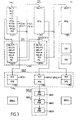
- the computer aided design system represented in Fig. 1 for the design of a device, more particularly of a chip, includes a computer COMP and a display unit DU with an associated keyboard KB and a pointing device or mouse M.
- the computer COMP comprises a processing unit CPU, coupled to the display unit DU, and a memory MEM storing a chip planner and builder programme CPBP comprising a code CPB and a data base DB, a graphics editor programme GERT, a procedural layout programme PLO and a routing programme RO.
- the latter programmes GERT, PLO and RO are able to work in cooperation with the programme CPBP, as will be explained later.
- the programme CPBP is an interactive programme which allows a user to interact with the system through the keyboard KB and with the mouse M which controls the position of a cursor on the DU. By operating a button on the mouse M the coordinates of a point designated by the cursor on the DU are entered in the memory MEM. This operation is called digitizing. Menus of instructions and parameters are displayed on the DU and the programme asks the user for additional information whenever this is required.
- the CPBP allows a user during a chip planning phase to realise and display on the unit DU the plan of a multi-layer chip in hierarchical levels and from the highest to the lowest level, and then to make the real layout of the thus planned chip during a following chip building phase. This is done from the lowest to the highest level. More particularly, the programme CPBP allows the plan of the chip to be realised by means of functional cells which are so arranged in a plurality of levels that the cell of highest level is the chip itself and that a cell of any other level forms part of a cell of the immediately higher level.
- the cells of lowest level i.e. those which are not further decomposed, are called leaf cells. These generally consist of arrays of simular cells.
- the above mentioned graphics editor programme GERT is used in the chip building phase and serves to introduce the real circuit layout in the leaf cells. During the rest of this phase the chip is gradually built up by means of data already provided by the user in the chip planning phase. This layout is stored in a file NGDF of the data base DB.
- the routing programme RO is a programme which may be used to create routes between the above mentioned functional cells.
- the programme CPBP may also be controlled from a command file provided by the procedural layout programme PLO, as will be explained later.
- each cell which is placed in another cell is considered as an instance of the definition of the first mentioned cell.
- the cell definition is independent from the placement, whereas the instance is dependent from this placement. Therefore the elements constituting the cell definition are defined with respect to the cell itself, whereas the elements defining the instance are defined with respect to the cell definition wherein this cell instance is placed.
- a cell definition may include an outline, terminals on that outline, and inside this outline connections and cuts.
- the cell instances are defined by their position and orientation inside the cell definition wherein they are placed. They mav be arranged in arrays and the terminals as well as the cuts may be assembled in busses.
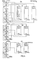
- Fig. 2 shows the two upper levels of a hierarchical plan of a multi-layer chip including several functional levels.
- Cell definition Cl has a point outline POL defined by the vertices P1 to P4, terminals T11 to T13 on that outline, and inside this outline a cut CUll and connections to be considered later.
- the cell definition of the cell instance CI21 has a point outline POL defined by the vertices P5 to P10 and terminals T21 and T22 on that outline, whilst the cell definition of the cell instance CI31 has a point outline POL defined by the vertices Pll to P14 and terminals T31 and T32 on that outline.
- the cell definition of the cell CI21 also has an outline defined by the contiguous boxes B21, B22 and B23 covering the surface of this cell.
- the chip plan shown in Fig. 2 may be gradually built up by the execution of the interactive programme CPBP, as will be described later.
- the data base DB is gradually constructed in such a way that it reflects the hierarchical plan of the chip.
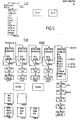
- the DB comprises a plurality of records corresponding to the abovs mentioned elements of a cell, i.e.:
- the data stored in the record CIR relate to the placement of cell definitions as instances in other cell definitions.
- the data stored in the other data records relate to elements of cell definitions which are independent from such a placement.
- the data base DB further includes or may include the following data blocks:
- the above data records and stores also include pointers by means of which they are interlinked.
- the function of each of the pointers is schematically indicated by a line leading to the data block to which it refers.
- the contents of these records and stores are considered hereinafter for the chip plan represented in Fig. 2. Therein absent or false data are indicated by 0.
- This record comprises the cell definition data blocks DC1, DC2 and DC3 which store data concerning the respective cell definitions Cl, C2 and C3 and various pointers to datablocks concerning elements of these definitions. For each cell definition these data are the following:
- the Cell Instance Record CIR (Fig. 3)
- This record may comprise sets CIR1, CIR2, CIR3 of interlinked instance data blocks which store data relating to the cell instances placed in the respective cell definitions Cl, C2 and C3.
- the data stored in each data block of such a set are the following:
- the Cell Outline Record COLR (Figs. 3, 4)
- this record comprises a Cell Point Outline Record CPOLR, a Cell Box Outline Record CBOLR, and a Pointer Record POL for the Outline.
- the Cell Point Outline Record CPOLR (Fig. 4)
- This record comprises the sets of point outline data blocks DPOL1, DPOL2 and DPOL3 which store data relating to the point outlines of the respective cell definitions Cl, C2 and C3.
- Each of the data blocks of a set stores the following data for a point of the cell definition point outline defined by this set:
- This record may comprise sets DBOL1, DBOL2 and DBOL3 of box outline data blocks which store data concerning the box outlines of the respective cell definitions Cl, C2 and C3.
- Each of the data blocks of a set stores the following data for a box of the cell box outline defined by this set:
- This record comprises the pointer blocks PB1, PB2 and PB3 which are associated to the respective cell definitions Cl, C2 and C3 and which store each the following pointers:
- the Cell Terminal Record CTR (Fig. 4)
- This record comprises sets DT1, DT2 and DT3 of terminal data blocks which store data concerning the terminals on the point outline of the respective cell definitions Cl, C2 and C3.
- the data blocks associated to terminals of a series located between two successive points of the outline are interlinked.
- Each of the data blocks of a set stores the following data for each terminal on this outline:
- the Cell Cut Record CCUR (Fig. 5)
- This record may comprise sets DCU1, DCU2, DCU3 of cut blocks which store data concerning cuts in the respective cell definitions C1, C2 and C3. Each of these data blocks of a set stores the following data for each cut belonging to this cell definition:
- This record may comprise the sets DCON1, DON2 and DCON3 of connection data blocks which store data concerning connections in the corresponding cell definitions Cl, C2 and C3. Each of these data blocks of a set stores the following data for each connection belonging to this cell definition:
- the NNDF (Fig. 5) is a file storing a net list for each of the cell definitions.
- the net list for the cell definition Cl comprises:
- An array header AH (Fig. 5) contains the following data:
- a terminal or cut bus header BTH or BCH (Fig. 5) is similar to an array header AH and includes the following data:
- CN Cl and ES are more particularly entered in the cell definition data block DC1 (Fig. 3). From the parameters LD and ES the programme calculates the surface of the main cell Cl and derives therefrom a square main cell which is displayed on the unit DU. The user may then either maintain this cell by digitizing the width thereof by means of the mouse or reject it. In the latter case he may either digitize a new width, the programme then calculating a new height from the surface, or he may digitize the points P1 to P4 of the outline, as is supposed here.
- the programme also starts a so-called plot outline procedure by which the main cell Cl is subdivided into a plurality of contiguous squares or rectangles, called boxes, defining the box outline.
- the data concerning these rectangles are stored in the Record DBOL1 (Fig. 3) as will be described further for cell instance C12. Afterwards the point and box outlines of the main cell Cl are both displayed on the display unit DU. Only the point outline of Cl is represented in Fig. 2.
- the last three parameters are stored in the data block DCI21 (Fig. 3).
- the user then for instance digitizes the points P5 to P10 defining the point outline of the cell definition C2, and the programme determines the box outline of this cell definition, i.e. each time with respect to P5.
- These outlines are then both displayed on the DU, as shown in Fig. 2, the box outline comprising the boxes B21, B22 and B23.
- the coordinates VL of the digitized points P5 to P10 are stored in the data blocks DP5 to DP10 of the set DPOL2 forming part of the CPOLR (Fig. 4), whilst the parameters MM of the boxes B21, B22 and B23 are stored in the data blocks DB21, DB22 and DB23 of the set DBOL2 of the CBOLR (Fig. 3).
- each MM is constituted by the coordinates of the bottom left and top right points of a box, again with respect to P5.
- MM for B21 comprises the coordinates of P5 and P9
- MM for B22 comprises the coordinates of P18 and P19
- MM for B23 comprises the coordinates of P9 and P7.
- the user then goes to the level of the instance CI21 by starting the execution of the instruction "Edit Cell” and digitizing a point DP (Fig. 2) in this instance CI21.
- a point DP (Fig. 2) in this instance CI21.
- coordinates of the digitized point DP are compared with the above mentioned coordinates MM of the boxes of both instances CI21 and CI31 and until the box is found wherein the digitized point DP is located. In the present case it will be found that the point DP is located in box B22 forming part of the instance CI21.
- This instance is then edited i.e. its outline is given a predetermined colour.
- the terminals T21 and T22 are then added on the outline of the cell instance CI21.
- the corresponding parameters are stored in the data blocks DT21 and DT22 (Fig. 4).
- the user then returns to the previous level i.e. to that of the main cell by executing the instruction "Quit".
- the currently edited cells is left : when this cell is the main cell the user is ending his edit session, whereas otherwise the previously edited cell again becomes the currently editied cell. For this reason in the present case, the main cell Cl is again edited.
- the user then again goes to the level of the instance CI31 in the same way as described above for the instance CI21 and adds terminals T31 and T32 on the outline of this instance.
- the corresponding parameters are stored in the data blocks DT31 and DT32 (Fig. 4).
- connections T12 T31, T13 T22 and T21 CUll are then realised and displayed in a similar way by the execution of corresponding add instructions.
- the corresponding parameters are stored in the respective data blocks DCN12, DCN13, DCN14 and in the respective associated lists LP12, LP13, LP14.
- an "add connection instruction” is executed for realising and displaying the connection CU11 T31, it being supposed that the points of this connection are digitized.
- the data entered for this instruction are:
- plan of the chip is generally, but not completely, built from a higher level to a lowel level. Indeed, now and then one returns to the higher level.
- the other (not shown) levels of the hierarchic chip plan are then realized in a similar way until the level of the so-called leaf cells is reached.
- the real layout of the thus planned chip is then made in the course of the chip building phase.
- the layout of the leaf cells is introduced in these cells under the control of the programme GERT, this layout being for instance taken from the location of the NGDF indicated by the pointer PNGDF stored in the cell definition data block.
- the layout is further completed by making use of the layout information concerning terminals, cuts and connections already stored in the data base DB during the chip plan phase, i.e. TL, TD, TW; CL1, CL2; COL, COW.
- the data to be changed in the data base DB when the plan of the chip is modified is minimized.
- the placement of the instance CI31 in the cell definition Cl is changed by a "Move origin instruction" i.e. by replacing the cell origin P11 to another point P'll, so that the cell instance CI'31 with outline P'll-P'14 is obtained, the following must be executed in the data base DB
- Another advantage of the describer data base structure is that it contains net information which may be used to check if the connections which have finally been realized are those indicated by the net information.
- the first command file includes the following commands
- the CPBP In case two cells instances are made to abut in the way described above, the CPBP always asks the user if for these instances terminals coincide. In the affirmative it creates for these coinciding terminals in the data base a connection data block with an associated list of the type DCN15 and LP15 respectively. However, the latter list now obviously only includes a single point.
- the advantage of proceeding in this way is that when the two instances are displaced away from each other by a predetermined instruction, the CPBP maintains the connection between the previously coinciding terminals, just as was the case in the above described example wherein the origin of CI31 was displaced.
- a method is provided to automatically realise a connection between two instances : one makes the instances to abut in such a way that terminals thereof coincide and then moves these instances away from each other.
Landscapes
- Engineering & Computer Science (AREA)
- Computer Hardware Design (AREA)
- Physics & Mathematics (AREA)
- Theoretical Computer Science (AREA)
- Evolutionary Computation (AREA)
- Geometry (AREA)
- General Engineering & Computer Science (AREA)
- General Physics & Mathematics (AREA)
- Architecture (AREA)
- Design And Manufacture Of Integrated Circuits (AREA)
Priority Applications (1)
| Application Number | Priority Date | Filing Date | Title |
|---|---|---|---|
| BE2/60764A BE903083A (nl) | 1985-08-19 | 1985-08-19 | Computergesteund ontwerpsysteem. |
Applications Claiming Priority (2)
| Application Number | Priority Date | Filing Date | Title |
|---|---|---|---|
| BE2060764 | 1985-08-19 | ||
| BE2/60764A BE903083A (nl) | 1985-08-19 | 1985-08-19 | Computergesteund ontwerpsysteem. |
Publications (1)
| Publication Number | Publication Date |
|---|---|
| EP0213670A2 true EP0213670A2 (de) | 1987-03-11 |
Family
ID=3865765
Family Applications (1)
| Application Number | Title | Priority Date | Filing Date |
|---|---|---|---|
| EP86201418A Withdrawn EP0213670A2 (de) | 1985-08-19 | 1986-08-12 | Rechnergestütztes Entwurfssystem |
Country Status (2)
| Country | Link |
|---|---|
| EP (1) | EP0213670A2 (de) |
| JP (1) | JPS62111361A (de) |
Cited By (2)
| Publication number | Priority date | Publication date | Assignee | Title |
|---|---|---|---|---|
| GB2305269A (en) * | 1995-08-25 | 1997-04-02 | Motorola Israel Ltd | Developing a layout for a semiconductor circuit element |
| GB2373610A (en) * | 2000-11-10 | 2002-09-25 | Hewlett Packard Co | Memory efficient occurrence model design for VLSI CAD |
-
1986
- 1986-08-12 EP EP86201418A patent/EP0213670A2/de not_active Withdrawn
- 1986-08-19 JP JP61192225A patent/JPS62111361A/ja active Pending
Cited By (4)
| Publication number | Priority date | Publication date | Assignee | Title |
|---|---|---|---|---|
| GB2305269A (en) * | 1995-08-25 | 1997-04-02 | Motorola Israel Ltd | Developing a layout for a semiconductor circuit element |
| GB2373610A (en) * | 2000-11-10 | 2002-09-25 | Hewlett Packard Co | Memory efficient occurrence model design for VLSI CAD |
| US6823300B1 (en) | 2000-11-10 | 2004-11-23 | Hewlett-Packard Development Company, L.P. | Memory efficient occurrence model design for VLSI CAD |
| GB2373610B (en) * | 2000-11-10 | 2004-12-01 | Hewlett Packard Co | Memory efficient occurrence model design for VLSI CAD |
Also Published As
| Publication number | Publication date |
|---|---|
| JPS62111361A (ja) | 1987-05-22 |
Similar Documents
| Publication | Publication Date | Title |
|---|---|---|
| US6957407B2 (en) | Method and apparatus for detail routing using obstacle carving around terminals | |
| US5596704A (en) | Process flow diagram generator | |
| WO2001024111A1 (en) | Automatic routing system for pc board design | |
| JPH0550780B2 (de) | ||
| JPH07334565A (ja) | 物体の配置方法 | |
| EP0612023B1 (de) | Wegsuchverfahren für Netzdiagramm | |
| US5754177A (en) | Method and apparatus for selecting an edit object on a display screen | |
| JPH0421910B2 (de) | ||
| US5835917A (en) | Table forming apparatus employing a partial ruled survey for facilitated table formation | |
| EP0213670A2 (de) | Rechnergestütztes Entwurfssystem | |
| JP2007233565A (ja) | 設計支援プログラム | |
| JPH06251007A (ja) | 表データ入力装置 | |
| JPH0589187A (ja) | 図形処理装置 | |
| US7298382B1 (en) | Figure selection method, figure selection device, and storage medium storing figure selection program | |
| US7530038B2 (en) | Method and placement tool for designing the layout of an electronic circuit | |
| Nishioka et al. | A minicomputerized automatic layout system for two-layer printed wiring boards | |
| JP3760403B2 (ja) | 表示情報の重なり回避方法及びその重なり回避システム及びその重なり回避プログラム | |
| JP2819203B2 (ja) | 図面管理方法および装置 | |
| JP3312959B2 (ja) | 引出線自動作成方式 | |
| JPH07104876B2 (ja) | 設計支援方法及び設計支援装置 | |
| JP3147055B2 (ja) | 図形の検索方法、図形検索装置及び記録媒体 | |
| JPH08161359A (ja) | 寸法線自動編集方法 | |
| JP2005128265A (ja) | 小縮尺配管図形データの作成方法 | |
| JP2792260B2 (ja) | セル行列認識装置 | |
| JPS63133274A (ja) | 配線処理方式 |
Legal Events
| Date | Code | Title | Description |
|---|---|---|---|
| PUAI | Public reference made under article 153(3) epc to a published international application that has entered the european phase |
Free format text: ORIGINAL CODE: 0009012 |
|
| AK | Designated contracting states |
Kind code of ref document: A2 Designated state(s): AT BE CH DE FR GB IT LI LU NL SE |
|
| RAP1 | Party data changed (applicant data changed or rights of an application transferred) |
Owner name: INTERNATIONAL STANDARD ELECTRIC CORPORATION NEW Y Owner name: BELL TELEPHONE MANUFACTURING COMPANY NAAMLOZE VENN |
|
| RBV | Designated contracting states (corrected) |
Designated state(s): FR GB |
|
| RAP1 | Party data changed (applicant data changed or rights of an application transferred) |
Owner name: INTERNATIONAL STANDARD ELECTRIC CORPORATION NEW YO |
|
| RAP1 | Party data changed (applicant data changed or rights of an application transferred) |
Owner name: ALCATEL N.V. |
|
| STAA | Information on the status of an ep patent application or granted ep patent |
Free format text: STATUS: THE APPLICATION HAS BEEN WITHDRAWN |
|
| 18W | Application withdrawn |
Withdrawal date: 19880205 |
|
| RAP3 | Party data changed (applicant data changed or rights of an application transferred) |
Owner name: ALCATEL N.V. |
|
| RIN1 | Information on inventor provided before grant (corrected) |
Inventor name: GUEBELS, PIERRE-PAUL FRANCOIS M.M. Inventor name: VAN DER LOOCK, JOHANNES |