EP0213842A2 - Mechanismus für parallele Speicherdatenabholung und Befehlsausführung in einem Prozessor mit reduziertem Befehlssatz - Google Patents
Mechanismus für parallele Speicherdatenabholung und Befehlsausführung in einem Prozessor mit reduziertem Befehlssatz Download PDFInfo
- Publication number
- EP0213842A2 EP0213842A2 EP86306267A EP86306267A EP0213842A2 EP 0213842 A2 EP0213842 A2 EP 0213842A2 EP 86306267 A EP86306267 A EP 86306267A EP 86306267 A EP86306267 A EP 86306267A EP 0213842 A2 EP0213842 A2 EP 0213842A2
- Authority
- EP
- European Patent Office
- Prior art keywords
- data
- instruction
- memory
- file
- register
- Prior art date
- Legal status (The legal status is an assumption and is not a legal conclusion. Google has not performed a legal analysis and makes no representation as to the accuracy of the status listed.)
- Granted
Links
Images

Classifications
-
- G—PHYSICS
- G06—COMPUTING OR CALCULATING; COUNTING
- G06F—ELECTRIC DIGITAL DATA PROCESSING
- G06F9/00—Arrangements for program control, e.g. control units
- G06F9/06—Arrangements for program control, e.g. control units using stored programs, i.e. using an internal store of processing equipment to receive or retain programs
- G06F9/30—Arrangements for executing machine instructions, e.g. instruction decode
- G06F9/38—Concurrent instruction execution, e.g. pipeline or look ahead
- G06F9/3861—Recovery, e.g. branch miss-prediction, exception handling
-
- G—PHYSICS
- G06—COMPUTING OR CALCULATING; COUNTING
- G06F—ELECTRIC DIGITAL DATA PROCESSING
- G06F9/00—Arrangements for program control, e.g. control units
- G06F9/06—Arrangements for program control, e.g. control units using stored programs, i.e. using an internal store of processing equipment to receive or retain programs
- G06F9/30—Arrangements for executing machine instructions, e.g. instruction decode
- G06F9/38—Concurrent instruction execution, e.g. pipeline or look ahead
- G06F9/3824—Operand accessing
-
- G—PHYSICS
- G06—COMPUTING OR CALCULATING; COUNTING
- G06F—ELECTRIC DIGITAL DATA PROCESSING
- G06F9/00—Arrangements for program control, e.g. control units
- G06F9/06—Arrangements for program control, e.g. control units using stored programs, i.e. using an internal store of processing equipment to receive or retain programs
- G06F9/30—Arrangements for executing machine instructions, e.g. instruction decode
- G06F9/38—Concurrent instruction execution, e.g. pipeline or look ahead
- G06F9/3824—Operand accessing
- G06F9/3834—Maintaining memory consistency
Definitions
- Computers require significantly more time to execute an instruction which retrieves data from a main memory than to execute an instruction which makes no such storage reference.
- Storage references can markedly slow the performance of a computer. Accordingly, techniques for eliminating the time penalty for storage references are known to the art.
- One such technique is to execute instrutions simultaneously with the retrieval of data from memory. Precautions must be taken however to avoid errors caused by a so-called instruction dependency where execution of an instruction changes the contents of a memory location, but, before the change is effected, data is retrieved from that location for use by a subsequent instruction. In this case, the first instruction must be allowed to complete execution before retrieval of the data by the subsequent instruction.
- RISC reduced instruction-set computer
- RISCs pose two problems for the application of prior art techniques such as mentioned above.
- a RISC usually includes a relatively large general purpose file register for the storage of often-used data. It is desirable to provide a separate data path from main memory into each register of the file so that data retrieved from storage may be written to any register within the file at the same time that data which results from the execution of an instruction is written to the file. Any delay in the writing is undesirable as it undermines the time improvement realized by the simultaneous data reference and instruction execution.
- the relatively large number of registers in a RISC file register makes the implementation of the separate data path uneconomical.
- RISC's omit the microcode level of processor control. Since the availability of microcode programming is often used to handle memory page faults through an interrupt procedure, RISC's must provide alternatives in both hardware and the software at the instruction set level to meet demand paging requirements.
- the described embodiment of the invention provides a simple architecture to implement a mechanism for performing data references to storage in parallel with instruction execution.
- the architecture is particularly suited to RISCs and employs a channel address register to store the main memory load or store address, a channel data register which temporarily stores the data for a store operation and, a channel control register which contains control information including the number of the register loaded within the file, in the case of a load operation. This number is used to detect instruction dependency of the data to be loaded.
- Logic circuitry suspends further instruction processing if the data required from a load is not yet available.
- a data-in register is used to store load data until an instruction execution cycle is available for writing it back to the register file. This technique eliminates the need for a separate path into the register file. Logic circuitry detects storage of data prior to its writing back, so as to effectively replace the register file location.
- the digital processor control portion 10 of a reduced instruction set computer is shown in block diagram form in Fig. 1 which provides data references to storage simultaneously with instruction execution.
- Processor 10 includes a register file 12 which is intended for storage of often-used data.
- a register file suitable for use in processor 10 is described in our European patent application number (case AMD 371).
- Fig. 1 illustrate only the data flow between the indicated elements and are capable of conducting several signals in parallel. Control signal paths are also required, as will be appreciated by those skilled in the art, but are not shown in Fig. 1 because it is well known by those skilled in the art how to effect control of the various illustrated elements.
- the register file 12 includes a set of registers each with a location designator or number.
- the register file 12 has a first and a second read port, a first and a second read address port, and a write port.
- the contents of a register within file 12 transferred to the first read port is conducted via a bus 14 to a data latch 16 and that transferred to the second read port is conducted via a bus 18 to a data latch 20.
- An output terminal of data latch 16, respectively, data latch 20, is connected via a bus 22, 24 respectively, to a first, second, respectively, input to an arithmetic/logic unit (ALU) 26.
- An output terminal of ALU 26 is connected to a second input terminal of latch 16 and latch 20 via a bus 28.
- Bus 28 also connects the output of ALU 26 to an input terminal of a data latch 30.
- An output terminal of latch 30 is connected via a bus 32 to the write port of register file 12.
- a portion of processor 10, not shown in Fig. 1, processes instructions fetched from an instruction cache, not shown, and causes the execution of actions called for by the instructions.
- Such action may include the loading of one of the data latches 16 or 20 from a register in file 12. The address of the particular register is specified by the instruction.
- Such action may be the storing of the results of an ALU 26 operation held in latch 30 into a register in file 12. Again, the address is specified by the instruction.
- These actions are controlled by a portion of the processor 10 not shown in Fig. 2, as will be appreciated by those skilled in the art. Reference can be had to the related, patent application for a detailed description of these operations.
- a main memory 34 is used by the processor 10 to store less-frequently needed data.
- a bidirectional data bus 36 connects memory 34 to a local channel 38 which serves processor 10. Other processors, not shown, may share memory 34 with processor 10. If so, they would be connected to memory 34 via their own local channels.
- An input terminal of a data-in register 40 is connected to local channel 38 so that load data retrieved from memory 34 can be temporarily stored.
- An output terminal of data-in register 40 is connected to an input terminal of latches 16, 20 and 30 via a bus 42.
- An input terminal of a channel address register 44 is connected via a bus 46 to the first read port of register file 12 and an input terminal of a channel data register 48 is connected via a bus 50 to the second read port of register file 12.
- Output terminals of the channel address and channel data registers 44 and 48 are connected to the local channel 38 via busses 52 and 54, respectively.
- a channel control register 56 receives status and control signals from the control portion of processor 10 and generates signals via signal lines 58 which maintain communication between the elements connected to the local channel 38.
- the control portion of processor 10 During the decode cycle of a load or a store instruction, the control portion of processor 10 generates signals which causes the storage address to be generated at the second read port of the register file 12, and data in the case of a store instruction, to be generated at the first read port of the register file 12 and at the end of the decode cycle, the address is conducted via bus 46 to channel address register 44, the data is conducted via bus 50 to channel data register 48, and control information is placed in the channel control register 56.
- the contents of registers 44, 48 and 56 are not changed until completion of the storage reference to memory 34, so that if a memory 34 page fault occurs before completion, the contents of these registers may be saved and used to restart the operation which caused the bus to detect a fault.
- execution of an instruction by the ALU 26 and related portions of processor 10 can occur independently and simultaneously with transfer of data from the main memory 34 via data-in register 40 and to the main memory via channel address and data registers 44 and 48, under control of the channel control register 56 and the control portion of processor 10.
- the number of the register in file 12 stored in channel control register 56 is also used to detect an instruction "depending" on the data to be loaded which may preclude simultaneous data references to storage and instruction execution.
- a comparator 60 receives on a first and a second signal line 62 and 64, signals representing, respectively, the register number of an operand to be retrieved from the file 12 and the register number of the register within file 12 which is the destination of an in-progress load, i.e., will be used to load the operand. Signals on lines 62 and 64 are also applied to the first and second read address ports, respectively, of register file 12. Comparator 60 also receives control signals from channel control 56 via signal lines 58 indicative of a register number within file 12 of any load which is in-progress.
- Comparator 60 generates at an output terminal a HIGH HOLD signal if the comparison of the register numbers conducted along lines 62 or 64 results in a match with that conducted along line 58, and further processing of the instruction retrieving the operand is suspended until the load in-progress is completed.
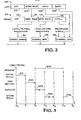
- FIG. 2 illustrates the execution of storage reference instructions, for a better understanding of the operation of the processor 10 during loading and storage of data to main memory 34.
- a portion 100 of a load instruction is shown consisting of an operation code 102, a register location number 104 identifying a location within file 12 of a memory 34 source address, the control information 106, and a destination address within register file 12 108.
- a source address is stored in the register within file 12 at a location identified by location number 104 for later transfer to the channel address register 44, the control information 106 and destination address 108 are stored in the channel control register 56 along with processor status information.
- a portion 110 of a store instruction is shown in Fig. 2 consisting of an operation code 112, a register location number 114 identifying a location within file 12 of a memory 34 source address, the register location number of the source of data to be retrieved from register file 12 116 and the control information 118.
- a source address is stored in the register file 12 at location identified by location number 114 for later transfer to the channel address register 44
- the data source is stored in the register file 12 at location identified by location number 116 for later transfer to the channel data register 48
- the control information 118 is stored in the channel control register 56. In this manner data can be loaded from main memory 34 to register file 12, and stored into main memory 34 from register file 12, simultaneously with instruction execution.
- Instruction dependencies are detected by the comparator 60 described above and prevent further execution of an instruction until a load is completed, if a dependency is detected.
- the contents of the registers 44, 48 and 56 can be used to resolve and restart the faulting operation.
- data retrieved from main memory 34 is conducted via bus 36 and local channel 38 to the data-in register 40 where it is stored until an instruction execution cycle is available in which the data may be written to the register file 12.
- the operation and architecture of processor illustrated in Fig. 1 eliminates the need for such separate paths. While the data resides in the data-in register 40, the comparators which detect instruction dependencies, described above, control the source of this data for use by the ALU 26.
- the contents of the data-in register 40 is conducted to either the first or second inputs of the ALU 26 via bus 42 and data latches 16 and 20, respectively, so that the data-in register 40 effectively replaces the register within file 12 which is the destination of the data retrieved from main memory 34.
- the processor 10 employs a four stage pipeline for the processing of instructions; fetch instruction from an instruction cache, decode instruction, execute the instruction, and store results.
- Fig. 3 is a timing diagram which illustrates simultaneous storage data references and execution of instructions provided by the processor 10
- the processor 10 can initiate transfers of data 205 from the register file 12 to the main memory 34 also beginning at time t 2 , so as to occur during the cycle immediately following the execution 203 of an instruction, beginning at to.
- the store back operation must occur after the main memory transfer operation 205 finishes, at time to, thus a delayed store back operation 206 begins at to and continues until t&. Additionally, a transfer of data from main memory 34 to file 12 can occur during the period t 3 to t b , simultaneous with the delayed store back operation 206.
Landscapes
- Engineering & Computer Science (AREA)
- Software Systems (AREA)
- Theoretical Computer Science (AREA)
- Physics & Mathematics (AREA)
- General Engineering & Computer Science (AREA)
- General Physics & Mathematics (AREA)
- Advance Control (AREA)
- Multi Processors (AREA)
- Memory System Of A Hierarchy Structure (AREA)
- Executing Machine-Instructions (AREA)
Priority Applications (1)
| Application Number | Priority Date | Filing Date | Title |
|---|---|---|---|
| AT86306267T ATE81730T1 (de) | 1985-08-30 | 1986-08-14 | Mechanismus fuer parallele speicherdatenabholung und befehlsausfuehrung in einem prozessor mit reduziertem befehlssatz. |
Applications Claiming Priority (2)
| Application Number | Priority Date | Filing Date | Title |
|---|---|---|---|
| US771435 | 1985-08-30 | ||
| US06/771,435 US4734852A (en) | 1985-08-30 | 1985-08-30 | Mechanism for performing data references to storage in parallel with instruction execution on a reduced instruction-set processor |
Publications (3)
| Publication Number | Publication Date |
|---|---|
| EP0213842A2 true EP0213842A2 (de) | 1987-03-11 |
| EP0213842A3 EP0213842A3 (en) | 1989-04-26 |
| EP0213842B1 EP0213842B1 (de) | 1992-10-21 |
Family
ID=25091809
Family Applications (1)
| Application Number | Title | Priority Date | Filing Date |
|---|---|---|---|
| EP86306267A Expired EP0213842B1 (de) | 1985-08-30 | 1986-08-14 | Mechanismus für parallele Speicherdatenabholung und Befehlsausführung in einem Prozessor mit reduziertem Befehlssatz |
Country Status (5)
| Country | Link |
|---|---|
| US (1) | US4734852A (de) |
| EP (1) | EP0213842B1 (de) |
| JP (1) | JP2539199B2 (de) |
| AT (1) | ATE81730T1 (de) |
| DE (1) | DE3686991T2 (de) |
Cited By (2)
| Publication number | Priority date | Publication date | Assignee | Title |
|---|---|---|---|---|
| EP0305639A3 (en) * | 1987-09-03 | 1990-02-28 | Director-General Of Agency Of Industrial Science And Technology | Vector computer |
| EP0288760A3 (de) * | 1987-03-27 | 1992-01-29 | Nec Corporation | Datenprozessor mit der Fähigkeit zur fehlerfreien Wiederausführung von Befehlen |
Families Citing this family (39)
| Publication number | Priority date | Publication date | Assignee | Title |
|---|---|---|---|---|
| US4814976C1 (en) * | 1986-12-23 | 2002-06-04 | Mips Tech Inc | Risc computer with unaligned reference handling and method for the same |
| US5317715A (en) * | 1987-12-15 | 1994-05-31 | Advanced Micro Devices, Inc. | Reduced instruction set computer system including apparatus and method for coupling a high performance RISC interface to a peripheral bus having different performance characteristics |
| US4926323A (en) * | 1988-03-03 | 1990-05-15 | Advanced Micro Devices, Inc. | Streamlined instruction processor |
| US5513332A (en) * | 1988-05-31 | 1996-04-30 | Extended Systems, Inc. | Database management coprocessor for on-the-fly providing data from disk media to all without first storing data in memory therebetween |
| JP3034873B2 (ja) * | 1988-07-01 | 2000-04-17 | 株式会社日立製作所 | 情報処理装置 |
| US5083263A (en) * | 1988-07-28 | 1992-01-21 | Sun Microsystems, Inc. | BISC with interconnected register ring and selectively operating portion of the ring as a conventional computer |
| US5226169A (en) * | 1988-12-30 | 1993-07-06 | International Business Machines Corp. | System for execution of storage-immediate and storage-storage instructions within cache buffer storage |
| JP2655191B2 (ja) * | 1989-07-05 | 1997-09-17 | 三菱電機株式会社 | 演算処理装置 |
| JP2816248B2 (ja) * | 1989-11-08 | 1998-10-27 | 株式会社日立製作所 | データプロセッサ |
| US5179681A (en) * | 1989-11-16 | 1993-01-12 | Sun Microsystems, Inc. | Method and apparatus for current window cache with switchable address and out cache registers |
| US5203002A (en) * | 1989-12-27 | 1993-04-13 | Wetzel Glen F | System with a multiport memory and N processing units for concurrently/individually executing 2N-multi-instruction-words at first/second transitions of a single clock cycle |
| AU629007B2 (en) * | 1989-12-29 | 1992-09-24 | Sun Microsystems, Inc. | Apparatus for accelerating store operations in a risc computer |
| AU7305491A (en) * | 1990-01-29 | 1991-08-21 | Teraplex, Inc. | Architecture for minimal instruction set computing system |
| US5210841A (en) * | 1990-01-30 | 1993-05-11 | Advanced Micro Devices, Inc. | External memory accessing system |
| US5222240A (en) * | 1990-02-14 | 1993-06-22 | Intel Corporation | Method and apparatus for delaying writing back the results of instructions to a processor |
| JP2553728B2 (ja) * | 1990-02-23 | 1996-11-13 | 松下電器産業株式会社 | 演算装置 |
| KR100210205B1 (ko) * | 1990-03-15 | 1999-07-15 | 리패치 | 스톨캐쉬를 제공하기 위한 장치 및 방법 |
| US5201056A (en) * | 1990-05-02 | 1993-04-06 | Motorola, Inc. | RISC microprocessor architecture with multi-bit tag extended instructions for selectively attaching tag from either instruction or input data to arithmetic operation output |
| US5179682A (en) * | 1990-05-15 | 1993-01-12 | Sun Microsystems, Inc. | Method and apparatus for improved current window cache with switchable address in, out, and local cache registers |
| US5226142A (en) * | 1990-11-21 | 1993-07-06 | Ross Technology, Inc. | High performance register file with overlapping windows |
| US5539911A (en) * | 1991-07-08 | 1996-07-23 | Seiko Epson Corporation | High-performance, superscalar-based computer system with out-of-order instruction execution |
| JPH0614003A (ja) * | 1991-07-31 | 1994-01-21 | Nec Corp | データ処理回路 |
| US5363495A (en) * | 1991-08-26 | 1994-11-08 | International Business Machines Corporation | Data processing system with multiple execution units capable of executing instructions out of sequence |
| EP0544083A3 (en) * | 1991-11-26 | 1994-09-14 | Ibm | Interleaved risc-type parallel processor and processing methods |
| US6735685B1 (en) * | 1992-09-29 | 2004-05-11 | Seiko Epson Corporation | System and method for handling load and/or store operations in a superscalar microprocessor |
| JP3644959B2 (ja) * | 1992-09-29 | 2005-05-11 | セイコーエプソン株式会社 | マイクロプロセッサシステム |
| US5434987A (en) * | 1993-09-21 | 1995-07-18 | Intel Corporation | Method and apparatus for preventing incorrect fetching of an instruction of a self-modifying code sequence with dependency on a bufered store |
| DE19506970A1 (de) * | 1995-02-28 | 1996-08-29 | Winkler Gmbh & Co Kg Baeckerei | Vorrichtung zum Fördern und Umsetzen von Teigstücken |
| US5878255A (en) * | 1995-06-07 | 1999-03-02 | Advanced Micro Devices, Inc. | Update unit for providing a delayed update to a branch prediction array |
| US5875324A (en) * | 1995-06-07 | 1999-02-23 | Advanced Micro Devices, Inc. | Superscalar microprocessor which delays update of branch prediction information in response to branch misprediction until a subsequent idle clock |
| US5898701A (en) * | 1995-12-21 | 1999-04-27 | Cypress Semiconductor Corporation | Method and apparatus for testing a device |
| US5805794A (en) * | 1996-03-28 | 1998-09-08 | Cypress Semiconductor Corp. | CPLD serial programming with extra read register |
| US5815510A (en) * | 1996-03-28 | 1998-09-29 | Cypress Semiconductor Corp. | Serial programming of instruction codes in different numbers of clock cycles |
| US5983321A (en) * | 1997-03-12 | 1999-11-09 | Advanced Micro Devices, Inc. | Cache holding register for receiving instruction packets and for providing the instruction packets to a predecode unit and instruction cache |
| US6122729A (en) * | 1997-05-13 | 2000-09-19 | Advanced Micro Devices, Inc. | Prefetch buffer which stores a pointer indicating an initial predecode position |
| US7024663B2 (en) * | 2002-07-10 | 2006-04-04 | Micron Technology, Inc. | Method and system for generating object code to facilitate predictive memory retrieval |
| US6954836B2 (en) | 2002-07-11 | 2005-10-11 | Micron Technology, Inc. | System and method for processor with predictive memory retrieval assist |
| US7290121B2 (en) * | 2003-06-12 | 2007-10-30 | Advanced Micro Devices, Inc. | Method and data processor with reduced stalling due to operand dependencies |
| WO2013105376A1 (ja) | 2012-01-13 | 2013-07-18 | オリンパスメディカルシステムズ株式会社 | 内視鏡先端部品および内視鏡 |
Family Cites Families (6)
| Publication number | Priority date | Publication date | Assignee | Title |
|---|---|---|---|---|
| US3771138A (en) * | 1971-08-31 | 1973-11-06 | Ibm | Apparatus and method for serializing instructions from two independent instruction streams |
| US4208716A (en) * | 1978-12-11 | 1980-06-17 | Honeywell Information Systems Inc. | Cache arrangement for performing simultaneous read/write operations |
| US4317168A (en) * | 1979-11-23 | 1982-02-23 | International Business Machines Corporation | Cache organization enabling concurrent line castout and line fetch transfers with main storage |
| JPS57100680A (en) * | 1980-12-15 | 1982-06-22 | Hitachi Ltd | Page fault processing system |
| US4439829A (en) * | 1981-01-07 | 1984-03-27 | Wang Laboratories, Inc. | Data processing machine with improved cache memory management |
| JPS59231652A (ja) * | 1983-06-13 | 1984-12-26 | Hitachi Ltd | メモリアクセス・オ−バラツプ検出方式 |
-
1985
- 1985-08-30 US US06/771,435 patent/US4734852A/en not_active Expired - Lifetime
-
1986
- 1986-08-14 DE DE8686306267T patent/DE3686991T2/de not_active Expired - Lifetime
- 1986-08-14 EP EP86306267A patent/EP0213842B1/de not_active Expired
- 1986-08-14 AT AT86306267T patent/ATE81730T1/de not_active IP Right Cessation
- 1986-08-28 JP JP61203572A patent/JP2539199B2/ja not_active Expired - Lifetime
Cited By (3)
| Publication number | Priority date | Publication date | Assignee | Title |
|---|---|---|---|---|
| EP0288760A3 (de) * | 1987-03-27 | 1992-01-29 | Nec Corporation | Datenprozessor mit der Fähigkeit zur fehlerfreien Wiederausführung von Befehlen |
| EP0305639A3 (en) * | 1987-09-03 | 1990-02-28 | Director-General Of Agency Of Industrial Science And Technology | Vector computer |
| US4967350A (en) * | 1987-09-03 | 1990-10-30 | Director General Of Agency Of Industrial Science And Technology | Pipelined vector processor for executing recursive instructions |
Also Published As
| Publication number | Publication date |
|---|---|
| EP0213842A3 (en) | 1989-04-26 |
| EP0213842B1 (de) | 1992-10-21 |
| JP2539199B2 (ja) | 1996-10-02 |
| DE3686991D1 (de) | 1992-11-26 |
| US4734852A (en) | 1988-03-29 |
| DE3686991T2 (de) | 1993-04-29 |
| ATE81730T1 (de) | 1992-11-15 |
| JPS6255736A (ja) | 1987-03-11 |
Similar Documents
| Publication | Publication Date | Title |
|---|---|---|
| US4734852A (en) | Mechanism for performing data references to storage in parallel with instruction execution on a reduced instruction-set processor | |
| US4811215A (en) | Instruction execution accelerator for a pipelined digital machine with virtual memory | |
| US4896259A (en) | Apparatus for storing modifying data prior to selectively storing data to be modified into a register | |
| US4187539A (en) | Pipelined data processing system with centralized microprogram control | |
| EP0689128B1 (de) | Kompression der Befehlswörter eines Rechners | |
| EP0071028B1 (de) | Instruktionsverarbeitungseinheit in einer Datenverarbeitungsanlage mit Instruktionssubstitution und Arbeitsverfahren | |
| US4296470A (en) | Link register storage and restore system for use in an instruction pre-fetch micro-processor interrupt system | |
| EP0491693B1 (de) | Cpu-pipeline mit registerfile-bypass durch adressvergleich bei aktualisierungen/zugriffen | |
| US4562538A (en) | Microprocessor having decision pointer to process restore position | |
| JPS6254342A (ja) | ディジタル命令プロセッサ制御装置および1サイクル内で分岐を実行する方法 | |
| JPH03116236A (ja) | 例外処理方法及び例外処理装置 | |
| JP2002328804A (ja) | データ処理装置、命令セット切換方法、データ処理アーキテクチャおよびデータ処理装置作動方法 | |
| US6003126A (en) | Special instruction register including allocation field utilized for temporary designation of physical registers as general registers | |
| US4279016A (en) | Instruction pre-fetch microprocessor interrupt system | |
| US6192461B1 (en) | Method and apparatus for facilitating multiple storage instruction completions in a superscalar processor during a single clock cycle | |
| EP0094535B1 (de) | Nach dem Prinzip der Pipeline arbeitendes Datenverarbeitungssystem | |
| EP0378415A2 (de) | Verteilungsmechanismus für mehrere Befehle | |
| US4773035A (en) | Pipelined data processing system utilizing ideal floating point execution condition detection | |
| US4394729A (en) | Jump return stack | |
| US6363474B1 (en) | Process switching register replication in a data processing system | |
| EP0010196B1 (de) | Kontrollschaltung und -verfahren für digitale Speicheranlagen | |
| US4093983A (en) | Fast and normal rate instruction fetching | |
| US5678016A (en) | Processor and method for managing execution of an instruction which determine subsequent to dispatch if an instruction is subject to serialization | |
| US5142630A (en) | System for calculating branch destination address based upon address mode bit in operand before executing an instruction which changes the address mode and branching | |
| EP0079370A4 (de) | Digitalrechner zur ausführung von befehlen in drei teilen in zeitmultiplex. |
Legal Events
| Date | Code | Title | Description |
|---|---|---|---|
| PUAI | Public reference made under article 153(3) epc to a published international application that has entered the european phase |
Free format text: ORIGINAL CODE: 0009012 |
|
| AK | Designated contracting states |
Kind code of ref document: A2 Designated state(s): AT BE CH DE FR GB IT LI LU NL SE |
|
| PUAL | Search report despatched |
Free format text: ORIGINAL CODE: 0009013 |
|
| AK | Designated contracting states |
Kind code of ref document: A3 Designated state(s): AT BE CH DE FR GB IT LI LU NL SE |
|
| 17P | Request for examination filed |
Effective date: 19890710 |
|
| 17Q | First examination report despatched |
Effective date: 19901126 |
|
| GRAA | (expected) grant |
Free format text: ORIGINAL CODE: 0009210 |
|
| AK | Designated contracting states |
Kind code of ref document: B1 Designated state(s): AT BE CH DE FR GB IT LI LU NL SE |
|
| REF | Corresponds to: |
Ref document number: 81730 Country of ref document: AT Date of ref document: 19921115 Kind code of ref document: T |
|
| ITF | It: translation for a ep patent filed | ||
| REF | Corresponds to: |
Ref document number: 3686991 Country of ref document: DE Date of ref document: 19921126 |
|
| ET | Fr: translation filed | ||
| PLBE | No opposition filed within time limit |
Free format text: ORIGINAL CODE: 0009261 |
|
| STAA | Information on the status of an ep patent application or granted ep patent |
Free format text: STATUS: NO OPPOSITION FILED WITHIN TIME LIMIT |
|
| PG25 | Lapsed in a contracting state [announced via postgrant information from national office to epo] |
Ref country code: LU Free format text: LAPSE BECAUSE OF NON-PAYMENT OF DUE FEES Effective date: 19930831 |
|
| 26N | No opposition filed | ||
| EAL | Se: european patent in force in sweden |
Ref document number: 86306267.5 |
|
| PGFP | Annual fee paid to national office [announced via postgrant information from national office to epo] |
Ref country code: SE Payment date: 19970717 Year of fee payment: 12 |
|
| PGFP | Annual fee paid to national office [announced via postgrant information from national office to epo] |
Ref country code: AT Payment date: 19970723 Year of fee payment: 12 |
|
| PGFP | Annual fee paid to national office [announced via postgrant information from national office to epo] |
Ref country code: BE Payment date: 19970908 Year of fee payment: 12 |
|
| PGFP | Annual fee paid to national office [announced via postgrant information from national office to epo] |
Ref country code: CH Payment date: 19971014 Year of fee payment: 12 |
|
| PG25 | Lapsed in a contracting state [announced via postgrant information from national office to epo] |
Ref country code: AT Free format text: LAPSE BECAUSE OF NON-PAYMENT OF DUE FEES Effective date: 19980814 |
|
| PG25 | Lapsed in a contracting state [announced via postgrant information from national office to epo] |
Ref country code: SE Free format text: LAPSE BECAUSE OF NON-PAYMENT OF DUE FEES Effective date: 19980815 |
|
| PG25 | Lapsed in a contracting state [announced via postgrant information from national office to epo] |
Ref country code: BE Free format text: LAPSE BECAUSE OF NON-PAYMENT OF DUE FEES Effective date: 19980831 Ref country code: LI Free format text: LAPSE BECAUSE OF NON-PAYMENT OF DUE FEES Effective date: 19980831 Ref country code: CH Free format text: LAPSE BECAUSE OF NON-PAYMENT OF DUE FEES Effective date: 19980831 |
|
| BERE | Be: lapsed |
Owner name: ADVANCED MICRO DEVICES INC. Effective date: 19980831 |
|
| REG | Reference to a national code |
Ref country code: CH Ref legal event code: PL |
|
| EUG | Se: european patent has lapsed |
Ref document number: 86306267.5 |
|
| REG | Reference to a national code |
Ref country code: GB Ref legal event code: IF02 |
|
| PGFP | Annual fee paid to national office [announced via postgrant information from national office to epo] |
Ref country code: GB Payment date: 20050707 Year of fee payment: 20 |
|
| PGFP | Annual fee paid to national office [announced via postgrant information from national office to epo] |
Ref country code: NL Payment date: 20050712 Year of fee payment: 20 |
|
| PGFP | Annual fee paid to national office [announced via postgrant information from national office to epo] |
Ref country code: FR Payment date: 20050804 Year of fee payment: 20 |
|
| PG25 | Lapsed in a contracting state [announced via postgrant information from national office to epo] |
Ref country code: IT Free format text: LAPSE BECAUSE OF NON-PAYMENT OF DUE FEES Effective date: 20050814 |
|
| PGFP | Annual fee paid to national office [announced via postgrant information from national office to epo] |
Ref country code: DE Payment date: 20050831 Year of fee payment: 20 |
|
| REG | Reference to a national code |
Ref country code: GB Ref legal event code: PE20 |
|
| PG25 | Lapsed in a contracting state [announced via postgrant information from national office to epo] |
Ref country code: GB Free format text: LAPSE BECAUSE OF EXPIRATION OF PROTECTION Effective date: 20060813 |
|
| PG25 | Lapsed in a contracting state [announced via postgrant information from national office to epo] |
Ref country code: NL Free format text: LAPSE BECAUSE OF EXPIRATION OF PROTECTION Effective date: 20060814 |
|
| NLV7 | Nl: ceased due to reaching the maximum lifetime of a patent |
Effective date: 20060814 |