EP0213902B1 - Procédés de fabrication de microtamis et microtamis ainsi obtenus - Google Patents
Procédés de fabrication de microtamis et microtamis ainsi obtenus Download PDFInfo
- Publication number
- EP0213902B1 EP0213902B1 EP86306526A EP86306526A EP0213902B1 EP 0213902 B1 EP0213902 B1 EP 0213902B1 EP 86306526 A EP86306526 A EP 86306526A EP 86306526 A EP86306526 A EP 86306526A EP 0213902 B1 EP0213902 B1 EP 0213902B1
- Authority
- EP
- European Patent Office
- Prior art keywords
- electrically conductive
- photoresist
- metal
- microsieve
- frame member
- Prior art date
- Legal status (The legal status is an assumption and is not a legal conclusion. Google has not performed a legal analysis and makes no representation as to the accuracy of the status listed.)
- Expired - Lifetime
Links
- 238000004519 manufacturing process Methods 0.000 title claims description 17
- 229920002120 photoresistant polymer Polymers 0.000 claims description 50
- 239000002184 metal Substances 0.000 claims description 37
- 229910052751 metal Inorganic materials 0.000 claims description 37
- 238000000034 method Methods 0.000 claims description 32
- 239000004020 conductor Substances 0.000 claims description 17
- 239000000758 substrate Substances 0.000 claims description 17
- PXHVJJICTQNCMI-UHFFFAOYSA-N Nickel Chemical compound [Ni] PXHVJJICTQNCMI-UHFFFAOYSA-N 0.000 claims description 16
- RYGMFSIKBFXOCR-UHFFFAOYSA-N Copper Chemical compound [Cu] RYGMFSIKBFXOCR-UHFFFAOYSA-N 0.000 claims description 12
- 229910052802 copper Inorganic materials 0.000 claims description 11
- 239000010949 copper Substances 0.000 claims description 11
- 229910052759 nickel Inorganic materials 0.000 claims description 8
- 239000012811 non-conductive material Substances 0.000 claims description 6
- 238000009713 electroplating Methods 0.000 claims description 4
- 239000011248 coating agent Substances 0.000 claims description 3
- 238000000576 coating method Methods 0.000 claims description 3
- 239000012188 paraffin wax Substances 0.000 claims description 2
- 229910000634 wood's metal Inorganic materials 0.000 claims description 2
- 229910001369 Brass Inorganic materials 0.000 claims 2
- 239000010951 brass Substances 0.000 claims 2
- 238000000151 deposition Methods 0.000 claims 1
- 210000004027 cell Anatomy 0.000 description 31
- PCHJSUWPFVWCPO-UHFFFAOYSA-N gold Chemical compound [Au] PCHJSUWPFVWCPO-UHFFFAOYSA-N 0.000 description 5
- 229910052737 gold Inorganic materials 0.000 description 5
- 239000010931 gold Substances 0.000 description 5
- 229910052709 silver Inorganic materials 0.000 description 5
- 239000004332 silver Substances 0.000 description 5
- BQCADISMDOOEFD-UHFFFAOYSA-N Silver Chemical compound [Ag] BQCADISMDOOEFD-UHFFFAOYSA-N 0.000 description 4
- 210000004698 lymphocyte Anatomy 0.000 description 3
- -1 etc. Inorganic materials 0.000 description 2
- 239000011888 foil Substances 0.000 description 2
- 239000000463 material Substances 0.000 description 2
- 229910001092 metal group alloy Inorganic materials 0.000 description 2
- 229910045601 alloy Inorganic materials 0.000 description 1
- 239000000956 alloy Substances 0.000 description 1
- 230000005540 biological transmission Effects 0.000 description 1
- 210000004369 blood Anatomy 0.000 description 1
- 239000008280 blood Substances 0.000 description 1
- 239000000969 carrier Substances 0.000 description 1
- 239000003795 chemical substances by application Substances 0.000 description 1
- 230000007812 deficiency Effects 0.000 description 1
- 230000001419 dependent effect Effects 0.000 description 1
- 238000004090 dissolution Methods 0.000 description 1
- 238000005530 etching Methods 0.000 description 1
- 238000007687 exposure technique Methods 0.000 description 1
- 239000012530 fluid Substances 0.000 description 1
- 230000000873 masking effect Effects 0.000 description 1
- 230000008018 melting Effects 0.000 description 1
- 238000002844 melting Methods 0.000 description 1
- 150000002739 metals Chemical class 0.000 description 1
- 239000000203 mixture Substances 0.000 description 1
- 230000004048 modification Effects 0.000 description 1
- 238000012986 modification Methods 0.000 description 1
- 230000002093 peripheral effect Effects 0.000 description 1
- 230000005855 radiation Effects 0.000 description 1
- 238000007873 sieving Methods 0.000 description 1
- 238000007711 solidification Methods 0.000 description 1
- 230000008023 solidification Effects 0.000 description 1
- 239000002904 solvent Substances 0.000 description 1
- 238000005406 washing Methods 0.000 description 1
- 238000005303 weighing Methods 0.000 description 1
- 239000002023 wood Substances 0.000 description 1
Images



Classifications
-
- C—CHEMISTRY; METALLURGY
- C25—ELECTROLYTIC OR ELECTROPHORETIC PROCESSES; APPARATUS THEREFOR
- C25D—PROCESSES FOR THE ELECTROLYTIC OR ELECTROPHORETIC PRODUCTION OF COATINGS; ELECTROFORMING; APPARATUS THEREFOR
- C25D1/00—Electroforming
- C25D1/08—Perforated or foraminous objects, e.g. sieves
Definitions
- This invention relates to improved methods for manufacturing extremely thin, very delicate metallic structures possessing grid-like patterns of minute, closely spaced, precisely dimensioned apertures.
- Such apertured metal structures hereinafter referred to as “microsieves” are especially useful in sorting and sieving objects of only a few microns in size.
- One such microsieve designated a “cell carrier” is described in Spanish Patent No. 522,207, granted June 1, 1984, and in commonly assigned, copending U.S. patent application Serial No. 550,233, filed November 8, 1983, the disclosure of which is incorporated by reference herein, for classifying biological cells by size.
- the cell carrier is prepared employing a modified photo-fabrication technique of the type used in the manufacture of transmission electron microscope grids.
- the cell carrier is on the order of only a few microns in thickness and possesses a numerically dense pattern of minute apertures. Even with the exercise of great care, the very delicate nature of the cell carrier makes it difficult to manipulate, for example, to insert it in a holder of the type shown in aforesaid U.S. patent application Serial No. 550,233, without causing it appreciable damage, frequently in the form of a structural deflection or deformation which renders it useless for its intended use.
- Fig. 1(a) is a plan view of the cell carrier
- Figs. 1(b) and 1(c) are perspective and side elevational views, respectively, of a typical section of the cell carrier
- Figs. 2(a) through 2(e) are side elevational views of successive steps in the manufacture of a section of the cell carrier.
- the cell carrier 10 shown in Fig. 1(a) is a very thin metallic disk, for example, about 8 to 10 microns in thickness, with a square-shaped, grid-like pattern of apertures 11 with centers about 15 microns apart defined within its geometric center.
- the cell carrier can be fabricated from a variety of metals including copper, nickel, silver, gold, etc., or a metal alloy.
- the apertures actually number 100 on a side for a total of 10,000 apertures and are thus able to receive, and retain, up to 10,000 cells of the desired size with each cell occupying a single aperture.
- Keyway 12 is provided to approximately orient the cell carrier within its holder.
- a representative section of grid 11 of cell carrier 10 possesses numerous apertures or holes 20 arranged in a matrix-like pattern of rows and columns along axes X and Y respectively. This arrangement makes it possible to label and locate any one aperture in terms of its position along coordinates X and Y.
- the shape of apertures 20 enables biological cells 21 of preselected dimensions to be effectively held to the carrier by applying means, such as a pressure differential between the upper and the bottom side of the carrier, or electromagnetic forces.
- carrier 10 is chosen to have apertures of sizes so that when the matter, for example, blood, containing the various cell groups is placed on carrier 10, most, if not all, of the apertures become occupied by cells of the group of interest with each aperture containing one such cell.
- the apertures can be sized to receive, say, lymphocytes of which there are two principal sizes, namely, those of 7 microns and those of 10-15 microns, with the former being the cells of most interest and the latter being washed away from the upper surface 10t of the grid under a continuous flow of fluid.
- apertures 20 will have an upper cross-sectional diameter of about 6 microns and a lower cross-sectional diameter of about 2 microns or so. In this way, a lymphocyte from the desired population of cells can easily enter an aperture but once it has occupied the aperture, it cannot pass out through the bottom side 10b of the carrier.
- the cut-out areas 30(d) about the bottom of each aperture have no functional significance and result from the procedures whereby the cell carrier is manufactured as discussed below in connection with Figs. 2(a) through 2(e).
- photoemulsion layer 30 has been selectively exposed to a source of actinic radiation employing a conventional mask procedure to produce a patterned surface of discrete areas of unexposed photoemulsion 30(a) surrounded by a continuous area 30(b) of exposed photoemulsion.
- mandrel 31 is removed and the fixed areas 30(a) of the photoemulsion are dissolved, or etched, away to provide carrier 10 containing the desired pattern, or grid, of apertures 20.
- a circumferential cut-away area 30(d) which possesses no role in the operation of the cell carrier is defined in the bottom of each aperture once fixed photoemulsion areas 30(a) are removed.
- the aforedescribed method for making a microsieve is subject to a number of disadvantages, foremost among them being the practical difficulty of providing a sufficient thickness, or aperture height, without simultaneously unduly reducing the numerical density of the apertures.
- the structure is mechanically very fragile and as a result, is difficult to manipulate without causing it to be distorted or damaged.
- Still another disadvantage lies in the fact that the sloping sides of apertures 20 make it easy for them to be occupied by more than one cell. Ideally, an essentially vertical slope is desired to prevent or minimize this possibility; however, such a slope cannot be obtained with the foregoing method.
- a method of making a microsieve comprising a grid-like array of microapertures arranged in a matrix-like pattern of rows and columns along respective X and Y axes, having improved rigidity and resistance to mechanical distortion such that the location of the microapertures along said X and Y axes is essentially permanent, which method comprises (a) applying a layer of photoresist to an electrically conductive substrate, (b) fixing preselected areas of the photoresist to provide a patterned surface in the form of a grid-like array of discrete areas of fixed photoresist, (c) removing the remaining photoresist to expose a continuous area of the electrically conductive substrate, (d) electroplating the substrate, and (e) removing the substrate and fixed photoresist to provide a finished microsieve; characterised in that each microaperture contains a cell-sized portion of controlled non-conical configuration such that said portion is adapted to hold one cell only, and further characterised in that
- the invention provides a microsieve in which the required rigidity is imparted thereto by the fact that it is integral with a rigid, self-supporting frame.
- the microsieve may be given the required rigidity by the fact that it has a greater thickness than has been disclosed in the prior art or by the fact that it is built up from successively laminated microlayers.
- a substantial proportion of the walls of the individual apertures may be essentially perpendicular to the microsieve surface.
- An ordinarily delicate microsieve may thus be provided with greater resistance to mechanical distortion by being integrally formed with a rigid frame or by having its thickness built up to an extent where it is significantly more capable of withstanding flex.
- microsieve may be formed as an integral part of a larger, frame member, it can be readily handled without significant risk of damage.
- microsieve as used herein shall be understood to include not only cell carriers and similar devices but other kinds of precision sieves, screens, grids, scales, reticules, and the like.
- Figure 3 is illustrative of a preferred microsieve in accordance with this invention shown generally at 10. As shown, the sides of apertures 20 are essentially vertical in contrast to the sloping sides of the apertures in the prior art microsieve of Figs. 1(a)-(c). This arrangement helps to lessen the opportunity for more than one cell to occupy more than one aperture and also minimizes distortion of the light path which can result in apertures with comparatively gentle sloping walls.
- Microsieve 10 of Fig. 3 is made by a modification of the known method illustrated in Figs. 2(a)-(e). Specifically, instead of laying down a thickness of photoresist 30 of only about 1 micron as in Fig. 2(a), the thickness of the photoresist layer is made to be about 7 microns or so. Thus, when the fixed areas of photoresist are eventually removed to provide the sieve, undercut areas 30(d) will actually have the straight-bore configuration shown in Fig. 3. In use, the undercut areas 30(d) of microsieve 10 face upwardly, i.e., toward upper face 40. At upper face 40, the diameter of apertures 20 is about 6 microns and in the constricted area 60, the diameter is about 2 microns; the diameter of the opening at under surface 50 of microsieve 10 is of no significance to the functioning of the device.
- Microsieve 10 of Figs. 4(a)-(f) illustrates still another embodiment of the present invention.
- surface 13a of rigid frame member 13 which is fabricated from an electrically conductive material such as copper, nickel, gold, silver, etc., is placed against a suitable nonadherent surface 11, e.g., one which is substantially optically flat, either directly thereon or indirectly upon a thin foil 12 which serves as a shim to separate surface 13a a short distance, e.g., 5 to 20 microns or so, from surface 11.
- Frame member 13 possesses a relatively large aperture 14, preferably circular in configuration and defined within the geometric center of surface 13a of the frame, filled with a hardenable electrically conductive material 15, e.g., Wood's alloy which solidifies below its melting point of about 65 o C, to form a smooth surface 17.
- Electrical contact 16 is inserted before, during or after hardening of electrically conductive material 15. Once electrically conductive material 15 has become hardened, i.e., by being cooled to below its solidification point, it will possess a smooth surface 17 of electrically conductive material corresponding to the configuration of the large aperture 14 and surrounded by surface 13a of frame member 13.
- surface 11 The sole function of surface 11 is to provide corresponding surface 17 of the electrically conductive material, when hardened, with a smooth, striation-free surface and that of optional foil 12 to extend surface 17 some short distance beyond surface 13a of frame 13. After electrically conductive material 15 has hardened, surface 13a of frame 13 is removed from contact with surface 11 and inverted to the face-up position as shown in Fig. 4(b).
- the height (or thickness) of photoresist 18 will be on the order of about 1 or 2 microns, the precise thickness being dependent in large measure upon the rheological properties of the particular photoresist selected.
- This electrodeposited metal 19 completely surrounds areas of fixed photoresist.
- electrically conductive material 15 is removed from frame member 13, usually with only a simple breaking-away action, and the fixed areas of photoresist are removed by dissolution or etching with an appropriate solvent to provide the finished, completely self-supporting microsieve spanning what had originally been large aperture 14 of frame member 13.
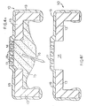
- copper frame member 13' of microsieve 10' initially does not possess an aperture.
- an etchant resistant, electrically non-conductive coating 20 is applied to the underside of frame member 13' except for an exposed, bare copper metal area 21 directly beneath the microsieve portion to be formed from electroplated nickel 19' layer.
- An etchant which selectively removes copper metal but which does not affect nickel is then used to remove central copper core 22 and fixed areas 18'b of photoresist are removed to provide a finished microsieve 10' similar to that shown in Fig. 4(f).
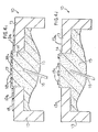
- central aperture 14 of frame member 13' is filled with a readily meltable or solvent-soluble electrically non-conductive material 30e, e.g., a paraffin wax, in place of electrically conductive material 15 of Fig. 4(a).
- a readily meltable or solvent-soluble electrically non-conductive material 30e e.g., a paraffin wax
- an electrically conductive metal 31a e.g., gold, silver, etc.
- Figs. 7(a) and (b) Another approach to imparting increased rigidity to a microsieve is illustrated in Figs. 7(a) and (b).
- the object is to build up the thickness of the microsieve body to the point where it becomes appreciably more resistant to flex, yet without sacrificing the numerical density of apertures.
- copper (or other electrically conductive metal) mandrel 40 possesses successive layers 41 to 53 of electroplated metal, e.g., nickel, surrounding fixed photoresist areas 53b which are in concentric alignment with the previously deposited areas of photoresist therebeneath.
- electroplated metal e.g., nickel
- This method of manufacturing a microsieve requires that each layer of electroplated metal be no higher, or thicker, than the adjacent areas of fixed photoresist.
- each of layers 41 to 53 can be separated by a layer 54 of vapor deposited metal of only a few angstroms thickness.
- the foregoing method makes it possible to vary the cross-sectional geometry of the apertures from one layer to the next and/or to stagger successive layers to obtain an aperture with a non-vertical bore.
Landscapes
- Chemical & Material Sciences (AREA)
- Organic Chemistry (AREA)
- Electrochemistry (AREA)
- Materials Engineering (AREA)
- Metallurgy (AREA)
- Engineering & Computer Science (AREA)
- Chemical Kinetics & Catalysis (AREA)
- Addition Polymer Or Copolymer, Post-Treatments, Or Chemical Modifications (AREA)
- Micromachines (AREA)
- Electroplating Methods And Accessories (AREA)
- Polysaccharides And Polysaccharide Derivatives (AREA)
- Gyroscopes (AREA)
- Weting (AREA)
- Photosensitive Polymer And Photoresist Processing (AREA)
- Filtering Materials (AREA)
Claims (18)
- Procédé de fabrication d'un micro-tamis, comprenant un groupement en grille de micro-ouvertures disposées en un canevas en forme de matrice, composé de rangées et de colonnes, le long d'axes X et Y respectivement, et possédant des qualités améliorées de rigidité et de résistance à la déformation mécanique, de telle manière que l'emplacement des micro-ouvertures selon lesdits axes X et Y soit sensiblement permanent, lequel procédé consiste : (a) à appliquer une couche de photorésist sur un substrat électroconducteur, (b) fixer des zones pré-sélectionnées du photorésist pour réaliser une surface dessinée sous la forme d'un groupement en grille de zones discrètes de photorésist fixé, (c) enlever le photorésist restant pour dénuder une surface continue du substrat électroconducteur, (d) revêtir le substrat d'un dépôt électrolytique, et (e) enlever le substrat et le photorésist fixé pour obtenir un micro-tamis fini ; caractérisé en ce que chaque micro-ouverture contient une partie, de la dimension d'une cellule, ayant une configuration non conique contrôlée, de telle manière que ladite partie soit adaptée pour contenir seulement une cellule, et caractérisé en outre en ce qu'au moins une des conditions suivantes (A), (B) et (C) est vérifiée : (A) ladite couche de photorésist est d'une hauteur d'au moins environ 6 microns ; (B) ledit substrat électroconducteur est d'une seule pièce avec un élément cadre rigide électroconducteur ; (C) dans la phase (d), un métal est déposé par dépôt électrolytique sur le substrat dénudé, sensiblement à la même hauteur ou épaisseur que les zones de photorésist fixé, pour donner naissance à une surface dessinée ayant la forme d'un groupement en grille, composée de petites zones de photorésist fixé, étroitement espacées, possédant des dimensions précises, entourées par une zone continue de métal déposé par dépôt électrolytique, et, avant la phase (e), une autre couche de photorésist est appliquée sur la surface dessinée, et la séquence de phases effectuée jusqu'à ce moment est répétée, une ou plusieurs fois, en faisant en sorte qu'à chaque répétition de la phase (b), les zones de photorésist fixé soient superposées aux zones de photorésist fixé obtenues précédemment, et dans un alignement prédéterminé avec ces zones, et que dans la dernière répétition de ladite séquence de phases, la phase (d) est omise.
- Procédé selon la revendication 1, dans lequel la condition (B) est vérifiée, et ledit substrat électroconducteur est préparé par les sous-phases consistant à :(i) préparer un élément cadre rigide, électroconducteur, ayant une ouverture relativement grande définie dans sa majeure surface, l'aire constituant la grande ouverture étant au moins égale à l'aire du groupement de micro-ouvertures en grille dans le micro-tamis fini ;(ii) remplir la grande ouverture d'une matière électroconductrice durcissable ; et(iii) laisser la matière électroconductrice durcir pour réaliser un substrat électroconducteur à surface lisse qui correspond à la configuration de la grande ouverture et entouré par l'élément cadre électro-conducteur.
- Procédé selon la revendication 2, dans lequel l'élément cadre électroconducteur est fabriqué en cuivre ou en laiton.
- Procédé selon la revendication 2 ou la revendication 3, dans lequel la matière électroconductrice durcissable est un métal de Wood.
- Procédé selon l'une quelconque des revendications 2 à 4, dans lequel la grande ouverture est définie par un cercle d'environ 1 000 à environ 3 000 microns de diamètre, le centre de l'ouverture étant fixé au centre géométrique de la majeure surface de l'élément cadre.
- Procédé selon l'une quelconque des revendications 2 à 5, dans lequel les zones discrètes de photorésist fixé sont d'une hauteur d'environ 1 à environ 2 microns, d'une largeur d'environ 7 à environ 11 microns et espacées l'une de l'autre d'une distance d'environ 15 à environ 25 microns, et il y a un nombre total d'environ 100 à environ 10 000 de ces zones discrètes de photorésist fixé.
- Procédé selon l'une quelconque des revendications 2 à 6, dans lequel le métal déposé par dépôt électrolytique est le nickel.
- Procédé selon l'une quelconque des revendications 2 à 7, dans lequel la matière électroconductrice durcie à surface lisse se prolonge sur une petite distance en dehors du plan de la surface environnante de l'élément cadre.
- Procédé selon l'une quelconque des revendications 2 à 8, dans lequel la surface lisse de la matière électroconductrice durcie est sensiblement d'une planéité optique.
- Procédé selon la revendication 1, dans lequel la condition (B) est vérifiée et ledit substrat électroconducteur est préparé par les sous-phases consistant à :(i) préparer un élément cadre rigide fabriqué en un premier métal électroconducteur et ayant des surfaces supérieure et inférieure continues ;(ii) appliquer sur la surface inférieure un revêtement non électroconducteur, qui est résistant à l'action d'un agent de gravure du métal de l'élément cadre, ledit revêtement entourant une zone libre de ladite surface inférieure qui se trouve directement au-dessous de la partie de la surface supérieure qu'il s'agit de munir du micro-tamis, la surface supérieure non revêtue formant le substrat voulu ;et, ensuite, dans la phase (d), le dépôt électrolytique est exécuté avec un deuxième métal qui diffère du premier métal ; et
dans la phase (e) le métal de l'élément cadre qui est situé directement au-dessous du métal déposé par dépôt électrolytique qui constituera le micro-tamis est sélectivement gravé, et finalement, le photorésist est enlevé. - Procédé selon la revendication 10, dans lequel le métal de l'élément cadre est le cuivre ou le laiton et le métal déposé par dépôt électrolytique est le nickel.
- Procédé selon la revendication 1, dans lequel la condition (B) est vérifiée et ledit substrat électroconducteur est préparé par les sous-phases consistant à :(i) préparer un élément cadre rigide, électroconducteur, ayant une ouverture relativement grande définie dans sa majeure surface, l'aire constituant la grande ouverture étant au moins égale à l'aire du groupement de micro-ouvertures en grille dans le micro-tamis fini ;(ii) remplir la grande ouverture d'une matière non électroconductrice durcissable ;(iii) laisser la matière non électroconductrice durcir pour former une matière non électroconductrice à surface lisse, correspondant à la configuration de la grande ouverture et entourée par l'élément cadre électroconducteur ; et(iv) déposer un métal électroconducteur par évaporation sur toute la surface combinée de la matière non conductrice entourée de la matière électroconductrice ;et, ensuite, la phase (e) est exécutée en enlevant la matière non électroconductrice de la grande ouverture pour dénuder le métal déposé par évaporation, enlever le métal déposé par évaporation ainsi dénudé, et enlever le photorésist fixé.
- Procédé selon la revendication 12, dans lequel la matière non électroconductrice est une cire de paraffine.
- Procédé selon la revendication 1, dans lequel la condition (c) est vérifiée et, en outre, des couches de métal déposées par évaporation sont interposées entre des couches successives de métal déposées par dépôt électrolytique.
- Procédé selon la revendication 1, dans lequel la condition (A) est vérifiée et les micro-ouvertures individuelles possèdent des parois sensiblement verticales jusqu'à une profondeur d'au moins environ 6 microns.
- Procédé selon l'une quelconque des revendications précédentes, dans lequel le photorésist est une émulsion photographique.
- Micro-tamis pouvant être préparé par le procédé selon l'une quelconque des revendications précédentes.
- Micro-tamis qui comprend un groupement de micro-ouvertures en grille agencé en un canevas en forme de matrice composé de rangées et de colonnes le long d'axes X et Y respectivement, possédant des qualités améliorées de rigidité et de résistance à la déformation mécanique, de telle manière que l'emplacement des micro-ouvertures selon lesdits axes X et Y soit sensiblement permanent et, dans lequel chaque micro-ouverture contient une partie de la dimension d'une cellule, ayant une configuration non conique contrôlée, de telle manière que cette partie soit adaptée pour contenir seulement une cellule.
Priority Applications (1)
| Application Number | Priority Date | Filing Date | Title |
|---|---|---|---|
| AT86306526T ATE102664T1 (de) | 1985-08-30 | 1986-08-22 | Herstellung von mikrosieben sowie nach diesem verfahren hergestellte mikrosiebe. |
Applications Claiming Priority (2)
| Application Number | Priority Date | Filing Date | Title |
|---|---|---|---|
| US06/771,315 US4772540A (en) | 1985-08-30 | 1985-08-30 | Manufacture of microsieves and the resulting microsieves |
| US771315 | 1985-08-30 |
Publications (3)
| Publication Number | Publication Date |
|---|---|
| EP0213902A2 EP0213902A2 (fr) | 1987-03-11 |
| EP0213902A3 EP0213902A3 (en) | 1988-09-21 |
| EP0213902B1 true EP0213902B1 (fr) | 1994-03-09 |
Family
ID=25091420
Family Applications (1)
| Application Number | Title | Priority Date | Filing Date |
|---|---|---|---|
| EP86306526A Expired - Lifetime EP0213902B1 (fr) | 1985-08-30 | 1986-08-22 | Procédés de fabrication de microtamis et microtamis ainsi obtenus |
Country Status (9)
| Country | Link |
|---|---|
| US (1) | US4772540A (fr) |
| EP (1) | EP0213902B1 (fr) |
| JP (1) | JPS62117610A (fr) |
| CN (1) | CN1004124B (fr) |
| AT (1) | ATE102664T1 (fr) |
| CA (1) | CA1309689C (fr) |
| DE (1) | DE3689701T2 (fr) |
| DK (1) | DK412586A (fr) |
| IL (1) | IL79807A (fr) |
Cited By (1)
| Publication number | Priority date | Publication date | Assignee | Title |
|---|---|---|---|---|
| DE10219584A1 (de) * | 2002-04-26 | 2003-11-20 | Fraunhofer Ges Forschung | Verfahren zur Herstellung von Mikrosieben |
Families Citing this family (28)
| Publication number | Priority date | Publication date | Assignee | Title |
|---|---|---|---|---|
| US5272081A (en) * | 1982-05-10 | 1993-12-21 | Bar-Ilan University | System and methods for cell selection |
| NL8603278A (nl) * | 1986-12-23 | 1988-07-18 | Stork Veco Bv | Membraan met perforaties en werkwijze voor het vervaardigen van een dergelijk membraan. |
| NL9002866A (nl) * | 1990-12-24 | 1992-07-16 | Stork Screens Bv | Werkwijze voor het vormen van een zeefmateriaal met lage inwendige spanning en aldus verkregen zeefmateriaal. |
| US5322763A (en) * | 1992-05-06 | 1994-06-21 | E. I. Du Pont De Nemours And Company | Process for making metal ledge on stencil screen |
| US5413668A (en) * | 1993-10-25 | 1995-05-09 | Ford Motor Company | Method for making mechanical and micro-electromechanical devices |
| US5573815A (en) * | 1994-03-07 | 1996-11-12 | E. I. Du Pont De Nemours And Company | Process for making improved metal stencil screens for screen printing |
| US6036832A (en) * | 1996-04-19 | 2000-03-14 | Stork Veco B.V. | Electroforming method, electroforming mandrel and electroformed product |
| US6210910B1 (en) | 1998-03-02 | 2001-04-03 | Trustees Of Tufts College | Optical fiber biosensor array comprising cell populations confined to microcavities |
| US7060431B2 (en) * | 1998-06-24 | 2006-06-13 | Illumina, Inc. | Method of making and decoding of array sensors with microspheres |
| KR100373056B1 (ko) * | 1999-09-04 | 2003-02-25 | 주식회사 유니테크 | 롤러 스크린 제조방법 |
| GB2354459B (en) * | 1999-09-22 | 2001-11-28 | Viostyle Ltd | Filtering element for treating liquids, dusts and exhaust gases of internal combustion engines |
| US7167615B1 (en) | 1999-11-05 | 2007-01-23 | Board Of Regents, The University Of Texas System | Resonant waveguide-grating filters and sensors and methods for making and using same |
| WO2001052968A1 (fr) * | 2000-01-24 | 2001-07-26 | Millipore Corporation | Separation physique de cellules par filtration |
| US20050158702A1 (en) * | 2000-09-05 | 2005-07-21 | Stuelpnagel John R. | Cellular arrays comprising encoded cells |
| US6495340B2 (en) * | 2000-11-28 | 2002-12-17 | Medis El Ltd. | Cell carrier grids |
| US20020143058A1 (en) | 2001-01-24 | 2002-10-03 | Taro Pharmaceutical Inductries Ltd. | Process for preparing non-hygroscopic sodium valproate composition |
| CA2513985C (fr) | 2003-01-21 | 2012-05-29 | Illumina Inc. | Moniteur de reactions chimiques |
| US20050019954A1 (en) * | 2003-07-23 | 2005-01-27 | Eastman Kodak Company | Photochromic dyes for microsphere based sensor |
| GB0513978D0 (en) * | 2005-07-08 | 2005-08-17 | Avecia Inkjet Ltd | Process |
| NL1030081C2 (nl) * | 2005-09-30 | 2007-04-02 | Stork Veco Bv | Zeefmateriaal uit metaal en werkwijze voor de vervaardiging daarvan. |
| SE533276C2 (sv) * | 2008-12-19 | 2010-08-10 | Alfa Laval Corp Ab | Centrifugalseparator med smörjanordning |
| SG185113A1 (en) * | 2010-05-04 | 2012-12-28 | Agency Science Tech & Res | A microsieve for cells and particles filtration |
| CN101905214A (zh) * | 2010-06-09 | 2010-12-08 | 李斌 | 一种高频振动筛筛体 |
| KR20180049826A (ko) * | 2011-10-14 | 2018-05-11 | 히타치가세이가부시끼가이샤 | 금속 필터의 제조 방법 |
| CN105135188B (zh) * | 2015-08-18 | 2018-01-19 | 南京中船绿洲机器有限公司 | 一种碟式分离机轴承润滑系统 |
| DE102018203065A1 (de) * | 2018-03-01 | 2019-09-05 | Robert Bosch Gmbh | Verfahren zur Herstellung eines Injektors |
| JP2019181352A (ja) * | 2018-04-06 | 2019-10-24 | 株式会社オプトニクス精密 | メッシュ部材 |
| CN110902642B (zh) * | 2018-09-17 | 2024-12-24 | 新科实业有限公司 | Mems封装件及制造其的方法 |
Family Cites Families (10)
| Publication number | Priority date | Publication date | Assignee | Title |
|---|---|---|---|---|
| US2968555A (en) * | 1958-01-13 | 1961-01-17 | Gen Motors Corp | Treatment of metal surfaces |
| US3139392A (en) * | 1959-08-10 | 1964-06-30 | Norman B Mears | Method of forming precision articles |
| US3329541A (en) * | 1960-05-20 | 1967-07-04 | Buckbee Mears Co | Method of forming fine mesh screens |
| NL260475A (fr) * | 1960-06-18 | |||
| GB1143611A (fr) * | 1965-03-22 | |||
| DE2512086C3 (de) * | 1975-03-19 | 1978-11-30 | Siemens Ag, 1000 Berlin Und 8000 Muenchen | Verfahren zur Herstellung freitragender, dünner Metallstrukturen |
| DE2832408A1 (de) * | 1978-07-24 | 1980-02-14 | Siemens Ag | Verfahren zur herstellung von praezisionsflachteilen, insbesondere mit mikrooeffnungen |
| US4388351A (en) * | 1979-08-20 | 1983-06-14 | Western Electric Company, Inc. | Methods of forming a patterned metal film on a support |
| US4415405A (en) * | 1981-08-19 | 1983-11-15 | Yale University | Method for engraving a grid pattern on microscope slides and slips |
| DD206924A3 (de) * | 1981-10-01 | 1984-02-08 | Mikroelektronik Zt Forsch Tech | Verfahren zum herstellen einer freitragenden abstandsmaske |
-
1985
- 1985-08-30 US US06/771,315 patent/US4772540A/en not_active Expired - Lifetime
-
1986
- 1986-08-22 DE DE3689701T patent/DE3689701T2/de not_active Expired - Fee Related
- 1986-08-22 AT AT86306526T patent/ATE102664T1/de not_active IP Right Cessation
- 1986-08-22 EP EP86306526A patent/EP0213902B1/fr not_active Expired - Lifetime
- 1986-08-22 IL IL79807A patent/IL79807A/xx not_active IP Right Cessation
- 1986-08-29 CA CA000517223A patent/CA1309689C/fr not_active Expired - Lifetime
- 1986-08-29 DK DK412586A patent/DK412586A/da not_active Application Discontinuation
- 1986-08-29 JP JP61205030A patent/JPS62117610A/ja active Pending
- 1986-08-30 CN CN86105330.3A patent/CN1004124B/zh not_active Expired
Cited By (1)
| Publication number | Priority date | Publication date | Assignee | Title |
|---|---|---|---|---|
| DE10219584A1 (de) * | 2002-04-26 | 2003-11-20 | Fraunhofer Ges Forschung | Verfahren zur Herstellung von Mikrosieben |
Also Published As
| Publication number | Publication date |
|---|---|
| CN1004124B (zh) | 1989-05-10 |
| CA1309689C (fr) | 1992-11-03 |
| CN86105330A (zh) | 1987-03-04 |
| US4772540A (en) | 1988-09-20 |
| EP0213902A3 (en) | 1988-09-21 |
| ATE102664T1 (de) | 1994-03-15 |
| JPS62117610A (ja) | 1987-05-29 |
| IL79807A (en) | 1990-09-17 |
| DK412586A (da) | 1987-03-01 |
| DK412586D0 (da) | 1986-08-29 |
| DE3689701T2 (de) | 1994-09-01 |
| EP0213902A2 (fr) | 1987-03-11 |
| IL79807A0 (en) | 1986-11-30 |
| DE3689701D1 (de) | 1994-04-14 |
Similar Documents
| Publication | Publication Date | Title |
|---|---|---|
| US4772540A (en) | Manufacture of microsieves and the resulting microsieves | |
| KR100880104B1 (ko) | 기판 상에 마이크로전자 스프링 구조체를 형성하는 방법 | |
| US4767418A (en) | Luminal surface fabrication for cardiovascular prostheses | |
| EP0604205B1 (fr) | Procédé de fabrication d'un cadre conducteur | |
| US20090025581A1 (en) | Mask for screen printing and screen printing method using the same | |
| US6036832A (en) | Electroforming method, electroforming mandrel and electroformed product | |
| US3703450A (en) | Method of making precision conductive mesh patterns | |
| US4379737A (en) | Method to make a built up area rotary printing screen | |
| US4675065A (en) | Method for securing a microsieve to a support member | |
| US4869714A (en) | Luminal surface fabrication for cardiovascular prostheses | |
| EP0141335B1 (fr) | Procédé pour la fabrication d'un masque pour rayon X avec couche métallique de support | |
| US5512161A (en) | Process for galvanically forming structured plate-shaped bodies | |
| US5944974A (en) | Process for manufacturing mold inserts | |
| US4564423A (en) | Permanent mandrel for making bumped tapes and methods of forming | |
| US5462648A (en) | Method for fabricating a metal member having a plurality of fine holes | |
| JP3865085B2 (ja) | 電鋳製品の製造方法 | |
| EP0894157B1 (fr) | Procede et matrice d'electroformage et produit ainsi obtenu | |
| GB2150596A (en) | Mesh structures especially for use in television camera tubes | |
| CA1217082A (fr) | Faconnage d'un pochoir | |
| JP3939785B2 (ja) | 電鋳製薄状金属板およびその製造方法 | |
| JP4674735B2 (ja) | 電鋳メタルの製造方法 | |
| JP2021184483A (ja) | メタルマスク | |
| KR100275372B1 (ko) | 회로기판 제조방법 | |
| KR100249317B1 (ko) | 미세 구조물 형성을 위한 리가 공정 | |
| JPH0627302A (ja) | 光学素子の母型およびその製造方法 |
Legal Events
| Date | Code | Title | Description |
|---|---|---|---|
| PUAI | Public reference made under article 153(3) epc to a published international application that has entered the european phase |
Free format text: ORIGINAL CODE: 0009012 |
|
| AK | Designated contracting states |
Kind code of ref document: A2 Designated state(s): AT BE CH DE FR GB IT LI LU NL SE |
|
| PUAL | Search report despatched |
Free format text: ORIGINAL CODE: 0009013 |
|
| AK | Designated contracting states |
Kind code of ref document: A3 Designated state(s): AT BE CH DE FR GB IT LI LU NL SE |
|
| 17P | Request for examination filed |
Effective date: 19890213 |
|
| 17Q | First examination report despatched |
Effective date: 19901025 |
|
| GRAA | (expected) grant |
Free format text: ORIGINAL CODE: 0009210 |
|
| AK | Designated contracting states |
Kind code of ref document: B1 Designated state(s): AT BE CH DE FR GB IT LI LU NL SE |
|
| REF | Corresponds to: |
Ref document number: 102664 Country of ref document: AT Date of ref document: 19940315 Kind code of ref document: T |
|
| REF | Corresponds to: |
Ref document number: 3689701 Country of ref document: DE Date of ref document: 19940414 |
|
| ET | Fr: translation filed | ||
| ITF | It: translation for a ep patent filed | ||
| PG25 | Lapsed in a contracting state [announced via postgrant information from national office to epo] |
Ref country code: GB Effective date: 19940822 Ref country code: AT Effective date: 19940822 |
|
| PG25 | Lapsed in a contracting state [announced via postgrant information from national office to epo] |
Ref country code: SE Effective date: 19940823 |
|
| PG25 | Lapsed in a contracting state [announced via postgrant information from national office to epo] |
Ref country code: LU Free format text: LAPSE BECAUSE OF NON-PAYMENT OF DUE FEES Effective date: 19940831 Ref country code: LI Effective date: 19940831 Ref country code: CH Effective date: 19940831 Ref country code: BE Effective date: 19940831 |
|
| PLBE | No opposition filed within time limit |
Free format text: ORIGINAL CODE: 0009261 |
|
| STAA | Information on the status of an ep patent application or granted ep patent |
Free format text: STATUS: NO OPPOSITION FILED WITHIN TIME LIMIT |
|
| EAL | Se: european patent in force in sweden |
Ref document number: 86306526.4 |
|
| BERE | Be: lapsed |
Owner name: BAR ILAN UNIVERSITY Effective date: 19940831 |
|
| 26N | No opposition filed | ||
| PG25 | Lapsed in a contracting state [announced via postgrant information from national office to epo] |
Ref country code: NL Effective date: 19950301 |
|
| NLV4 | Nl: lapsed or anulled due to non-payment of the annual fee | ||
| GBPC | Gb: european patent ceased through non-payment of renewal fee |
Effective date: 19940822 |
|
| PG25 | Lapsed in a contracting state [announced via postgrant information from national office to epo] |
Ref country code: FR Effective date: 19950428 |
|
| REG | Reference to a national code |
Ref country code: CH Ref legal event code: PL |
|
| PG25 | Lapsed in a contracting state [announced via postgrant information from national office to epo] |
Ref country code: DE Effective date: 19950503 |
|
| EUG | Se: european patent has lapsed |
Ref document number: 86306526.4 |
|
| REG | Reference to a national code |
Ref country code: FR Ref legal event code: ST |
|
| PG25 | Lapsed in a contracting state [announced via postgrant information from national office to epo] |
Ref country code: IT Free format text: LAPSE BECAUSE OF NON-PAYMENT OF DUE FEES;WARNING: LAPSES OF ITALIAN PATENTS WITH EFFECTIVE DATE BEFORE 2007 MAY HAVE OCCURRED AT ANY TIME BEFORE 2007. THE CORRECT EFFECTIVE DATE MAY BE DIFFERENT FROM THE ONE RECORDED. Effective date: 20050822 |