EP0214376A2 - Circuit pour une source de signaux à fréquences acoustiques et à faible bruit - Google Patents
Circuit pour une source de signaux à fréquences acoustiques et à faible bruit Download PDFInfo
- Publication number
- EP0214376A2 EP0214376A2 EP86107972A EP86107972A EP0214376A2 EP 0214376 A2 EP0214376 A2 EP 0214376A2 EP 86107972 A EP86107972 A EP 86107972A EP 86107972 A EP86107972 A EP 86107972A EP 0214376 A2 EP0214376 A2 EP 0214376A2
- Authority
- EP
- European Patent Office
- Prior art keywords
- circuit arrangement
- impedance
- zero
- noise
- amplifier
- Prior art date
- Legal status (The legal status is an assumption and is not a legal conclusion. Google has not performed a legal analysis and makes no representation as to the accuracy of the status listed.)
- Withdrawn
Links
- 230000003321 amplification Effects 0.000 claims description 6
- 238000003199 nucleic acid amplification method Methods 0.000 claims description 6
- 230000005540 biological transmission Effects 0.000 description 3
- 239000003990 capacitor Substances 0.000 description 3
- 238000010586 diagram Methods 0.000 description 3
- 230000000694 effects Effects 0.000 description 2
- 101100289200 Caenorhabditis elegans lite-1 gene Proteins 0.000 description 1
- 238000013459 approach Methods 0.000 description 1
- 239000012141 concentrate Substances 0.000 description 1
- 230000008878 coupling Effects 0.000 description 1
- 238000010168 coupling process Methods 0.000 description 1
- 238000005859 coupling reaction Methods 0.000 description 1
- 238000013461 design Methods 0.000 description 1
- 238000011161 development Methods 0.000 description 1
- 230000018109 developmental process Effects 0.000 description 1
- 230000001771 impaired effect Effects 0.000 description 1
- 230000007257 malfunction Effects 0.000 description 1
- 238000013507 mapping Methods 0.000 description 1
- 238000000034 method Methods 0.000 description 1
- 230000003313 weakening effect Effects 0.000 description 1
- 238000004804 winding Methods 0.000 description 1
Images
Classifications
-
- H—ELECTRICITY
- H03—ELECTRONIC CIRCUITRY
- H03H—IMPEDANCE NETWORKS, e.g. RESONANT CIRCUITS; RESONATORS
- H03H11/00—Networks using active elements
- H03H11/02—Multiple-port networks
- H03H11/28—Impedance matching networks
-
- H—ELECTRICITY
- H03—ELECTRONIC CIRCUITRY
- H03F—AMPLIFIERS
- H03F1/00—Details of amplifiers with only discharge tubes, only semiconductor devices or only unspecified devices as amplifying elements
- H03F1/56—Modifications of input or output impedances, not otherwise provided for
Definitions
- the invention relates to a circuit arrangement according to the preamble of patent claim 1.
- Such a circuit arrangement is described in DE-PS 29 25 049. It can be used with particular advantage when a microphone, for example a condenser microphone or dynamic microphone, preferably with a downstream transformer, which transforms the microphone output voltage up somewhat, is to be connected to a so-called zero-ohm or node amplifier;
- the invention is particularly useful when the zero-ohm amplifier is a controlled, in particular voltage-controlled, amplifier, that is to say a so-called VCA (Voltage Controlled Amplifier).
- VCA Voltage Controlled Amplifier
- DE-PS 29 25 049 relates to such a case, but the present invention can also be used with other VCAs in which an operational amplifier with non-linear negative feedback is usually provided in the input stage, as in the prior publication.
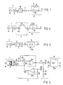
- a gain-controllable zero-ohm amplifier N is to be connected, which essentially consists of an operational amplifier OP with a controllable (variable) negative feedback resistor V.
- the zero ohm amplifier has a very ge wrestle input resistance of approximately 0 ohms, which would place an excessive load on the audio frequency source T.
- An impedance converter W is therefore interposed, the positive output resistance of which is substantially smaller than its input resistance, and the voltage amplification of which is chosen to be so small that its output range is not overdriven at its maximum input voltage.
- the series resistance is also responsible for the noise contribution that the operational amplifier OP itself makes: This noise contribution can be thought to be caused by a noise voltage source directly at the inverting input of the operational amplifier OP.
- the noise voltage of the noise voltage source is amplified by the operational amplifier connected to V and L with the so-called internal amplification of the zero-ohm amplifier N, which is greater the smaller the resistance value L is.
- the impedance converter W and the relatively small series resistance L still make such high noise contributions by increasing the internal amplification of the zero-ohm amplifier N that the zero-ohm amplifier would also have to be dimensioned with low noise if stricter demands for a still low-noise signal at the output of the zero-ohm amplifier should be met.
- a gain-controllable zero-ohm amplifier dimensioned accordingly low noise.
- the series resistance L in FIG. 1 should be as small as possible so that it makes a low noise contribution.
- this series resistance L should also have the greatest possible value in order to keep the internal gain small and also because it is good for another reason to ensure that the ratio of the resistance values V to L does not become too large, because at If the ratio of these values is too high, which in itself determines the gain of the negative feedback zero-ohm amplifier N, the negative feedback becomes so weak and the gain approaches the open-loop gain of the operational amplifier OP so far that the upper limit frequency of this open-loop gain becomes noticeable .
- the output of the impedance converter W would be largely short-circuited due to an insufficient value of the series resistance L and due to the low input resistance of the zero-ohm amplifier N, which would lead to its malfunction in a conventional impedance converter.
- the zero Ohm amplifier N would no longer receive a signal that is sufficiently high above the noise.
- the circuit arrangement according to the invention can be designed to be low-noise with less effort than, for example, a controllable zero-ohm amplifier, and secondly that it can be designed relatively simply in such a way that the zero-ohm amplifier is already sufficiently far above that Noise-producing, strong signal in the form of a current provides, and that thirdly it does not contribute appreciably to the increase in the internal gain of the zero-ohm amplifier.
- the impedance converter W and the series resistor L from Figure 1 are replaced by a circuit arrangement S with an input E and an output A.
- It is a short-circuit proof AC source, i.e. a source with a very high internal resistance K, which is fed by an equivalent voltage source UE, which supplies very high voltage values and which follows the voltage at input E.
- This alternating current source provides the zero-ohm amplifier N at point A with a signal which is sufficiently high above the noise in the form of a current, so that the inherent noise of the zero-ohm amplifier N is less important than in the arrangement according to Figure 1.
- the circuit arrangement S in FIG. 2 is to be designed with low noise, so that the equivalent noise resistance of the sound source T together with the downstream circuit arrangement S is at most 20%, preferably at most 10%, higher than the equivalent noise resistance of the sound source T alone.
- the internal resistance K which is indeed an AC voltage resistance
- the noise effect of this ohmic component can be imagined as follows: If the equivalent voltage source UE is short-circuited and a noise voltage source is substituted for the ohmic component of the internal resistance K, it can be seen that the relatively small noise voltage generated by it only has the very small ratio V to K is amplified by the zero ohm amplifier N.
- FIG. 3 is a block diagram. It shows that the circuit arrangement S contains two components, namely an infrasound filter F, also called impact sound filter, and the actual alternating current source U / I, which converts the voltage at the input E into a current converges at exit A.
- the zero-ohm amplifier N is shown as VCA, which can be controlled by a control voltage Us.
- a preferred embodiment of the circuit arrangement S is specified.
- the essential components are a first impedance converter W1, which is high-impedance on the input side, that is to say several powers of ten higher than the output side, and has a voltage gain of one. This is achieved by strong negative feedback via the negative input of the operational amplifier contained in the impedance converter W1.
- a series resistor R is connected downstream, on which the voltage Ue is shown.
- a second impedance converter W2 Arranged in a feedback path RW is a second impedance converter W2 of the same type as W1, which ensures the exact mapping of the voltage Ue across the series resistor R. In order to understand this, it must be considered that output A is practically at ground potential due to the VCA's zero-ohm input.
- W2 also keeps the terminal of the transformer U connected to the feedback path RW at ground potential.
- Signals Ue which come from the transmitter U, are mapped onto the series resistor R by the amplification of one of the impedance converter W1.
- the cause of the voltage Ue dropping across the series resistor R and representing the input voltage must be a current flowing through R. Since the series resistance R lies between the low-resistance output of W1 and the high-resistance input of W2, the current can only flow away via the input A of the zero-ohm amplifier N.
- the high impedance of the alternating current source formed by S can be clarified by considering that an alternating potential shift at A would also shift the potential at both terminals (via the transformer winding) of input E, to Ue and thus to the current through R but without influence remains.
- the circuit arrangement S shown forms a short-circuit-proof alternating current source which, with an alternating output current of at most 50 mA, effectively supplies the VCA with a signal which is so strong that no great demands have to be made on its freedom from noise. This also contributes to the fact that the circuit arrangement S itself only makes a small noise contribution.
- the source impedance of the audio frequency source T is 800 ohms.
- the equivalent noise resistance of the circuit arrangement S is added to the noise contributions thus made.
- the operational amplifiers each make contributions corresponding to an equivalent noise resistance of approximately 40 ohms.
- the effect of the series resistance R which can have, for example, 100 ohms. It should be chosen to be as small as possible with a view to noise, but it should also not be too small so that too much current does not flow into the VCA.
- the voltage gain of the circuit arrangement S is almost zero. Their inner signal swing corresponds to the maximum occurring input voltage. A range of 140 to 150dB is considered.
- the input impedance of the circuit arrangement S is at least ten times greater than the source impedance of the audio frequency source T, so that it is not overloaded and the signal-to-noise ratio is not significantly deteriorated by an unfavorable voltage divider ratio.
- the transmission ratio of the transmitter U is preferably 1: 2 (to 1: 3) in the case of a dynamic microphone and in the case of one Condenser microphone preferably about 1: 1.
- a larger transmission ratio would be desirable per se, but it then becomes difficult to process the large voltages occurring at the input E in the circuit arrangement S without distortion.
- An infrasound filter is also contained in the circuit arrangement S. It is a particular advantage of the invention and in particular of the exemplary embodiment according to FIG. 4 that this infrasound filter cannot be arranged behind the VCA as before, but is already in front of the positive input of the impedance converter W1. It consists of the two resistor-capacitor combinations R1-C1 and R2-C2. While it was possible with the arrangement of the impact sound filter behind the VCA that the preliminary stages were already overdriven by impact sound, this is avoided in the arrangement according to FIG. 4, and without the noise behavior of the circuit arrangement S being significantly impaired by the integrated impact sound filter.
- Another combination R3-C3 serves to improve the properties of the transformer Ü.
- resistors R4, R5 and a capacitor C6 are provided at the output A.
- R5 and C6 only serve to prevent the VCA from oscillating.
- the capacity of C6 is very low with an AC resistance that is smaller than R4 in the useful frequency range.
- This resistor R4 has a value of the order of 20 kOhm and is therefore dimensioned so high that it does not noticeably increase the internal gain of the zero-ohm amplifier N, i.e. preferably not increased by more than 10%.
Landscapes
- Engineering & Computer Science (AREA)
- Power Engineering (AREA)
- Amplifiers (AREA)
- Control Of Amplification And Gain Control (AREA)
Applications Claiming Priority (2)
| Application Number | Priority Date | Filing Date | Title |
|---|---|---|---|
| DE3531274 | 1985-09-02 | ||
| DE19853531274 DE3531274A1 (de) | 1985-09-02 | 1985-09-02 | Schaltungsanordnung fuer eine rauscharme tonfrequenzquelle |
Publications (2)
| Publication Number | Publication Date |
|---|---|
| EP0214376A2 true EP0214376A2 (fr) | 1987-03-18 |
| EP0214376A3 EP0214376A3 (fr) | 1989-03-22 |
Family
ID=6279924
Family Applications (1)
| Application Number | Title | Priority Date | Filing Date |
|---|---|---|---|
| EP86107972A Withdrawn EP0214376A3 (fr) | 1985-09-02 | 1986-06-11 | Circuit pour une source de signaux à fréquences acoustiques et à faible bruit |
Country Status (4)
| Country | Link |
|---|---|
| US (1) | US4725789A (fr) |
| EP (1) | EP0214376A3 (fr) |
| JP (1) | JPS6257304A (fr) |
| DE (1) | DE3531274A1 (fr) |
Families Citing this family (5)
| Publication number | Priority date | Publication date | Assignee | Title |
|---|---|---|---|---|
| WO1994017590A1 (fr) * | 1993-01-27 | 1994-08-04 | Micro Linear Corporation | Technique de circuit de reglage de la transductance |
| US20020183233A1 (en) * | 2000-12-14 | 2002-12-05 | The Clorox Company, Delaware Corporation | Bactericidal cleaning wipe |
| US20030100465A1 (en) * | 2000-12-14 | 2003-05-29 | The Clorox Company, A Delaware Corporation | Cleaning composition |
| US7799751B2 (en) * | 2000-12-14 | 2010-09-21 | The Clorox Company | Cleaning composition |
| KR20060117981A (ko) * | 2003-12-31 | 2006-11-17 | 쓰리엠 이노베이티브 프로퍼티즈 컴파니 | 발수성 및 발유성 플루오로아크릴레이트 |
Family Cites Families (5)
| Publication number | Priority date | Publication date | Assignee | Title |
|---|---|---|---|---|
| US3296544A (en) * | 1964-08-12 | 1967-01-03 | Ampex | Transistorized low noise preamplifier having high resistive input impedance and low input capacity |
| US3501711A (en) * | 1968-11-12 | 1970-03-17 | Textron Inc | Zero-voltage driven-cable amplifier |
| DE2711520C3 (de) * | 1976-03-16 | 1979-08-02 | Matsushita Electric Industrial Co., Ltd., Kadoma, Osaka (Japan) | Belastungsschaltung für eine Signalquelle |
| DE2811668C2 (de) * | 1978-03-17 | 1982-03-04 | Messerschmitt-Bölkow-Blohm GmbH, 8000 München | Anpassungsschaltung für hochohmige Spannungsquellen |
| DE2925049C2 (de) * | 1979-06-19 | 1982-03-25 | Licentia Patent-Verwaltungs-Gmbh, 6000 Frankfurt | Verstärker für eine Signalquelle hoher Dynamik |
-
1985
- 1985-09-02 DE DE19853531274 patent/DE3531274A1/de not_active Withdrawn
-
1986
- 1986-06-11 EP EP86107972A patent/EP0214376A3/fr not_active Withdrawn
- 1986-08-29 US US06/901,620 patent/US4725789A/en not_active Expired - Fee Related
- 1986-09-02 JP JP61205248A patent/JPS6257304A/ja active Pending
Also Published As
| Publication number | Publication date |
|---|---|
| EP0214376A3 (fr) | 1989-03-22 |
| US4725789A (en) | 1988-02-16 |
| DE3531274A1 (de) | 1987-03-12 |
| JPS6257304A (ja) | 1987-03-13 |
Similar Documents
| Publication | Publication Date | Title |
|---|---|---|
| DE60009656T2 (de) | Verstärkerschaltung | |
| DE2236709C2 (de) | Einstellbares Bandpaßfilter | |
| DE69520862T2 (de) | Detektorzelle für logarithmische Verstärker | |
| DE2658301C2 (de) | Hörgerät | |
| DE2003040A1 (de) | Elektrokardiographie-Verstaerker | |
| DE102004052174B4 (de) | Verstärkerschaltung, umfassend einen Verstärker mit tiefpassgefilterter Rückkopplung | |
| DE2618268C3 (de) | Verfahren zur Kompression eines Signals und zur Expansion des komprimierten Signals sowie Anordnung zur Durchführung des Verfahrens | |
| DE19525411A1 (de) | Signalverstärker | |
| EP0214376A2 (fr) | Circuit pour une source de signaux à fréquences acoustiques et à faible bruit | |
| EP1374392B1 (fr) | Montage amplificateur | |
| DE2747415A1 (de) | Rauschunterdrueckungsvorrichtung | |
| DE60011475T2 (de) | Aktives isolierter integratortiefpassfilter mit dämpfungspolen | |
| DE2423475C2 (de) | Schaltungsanordnung zur Änderung des dynamischen Bereichs eines Nachrichtensignals | |
| DE102004005986A1 (de) | Aktiver Filterschaltkreis | |
| DE493123C (de) | Anordnung zur Regelung des UEbertragungsgrades in von Wechselstroemen durch-flossenen Signalsystemen mit Verstaerkern | |
| DE2937912C2 (de) | Operationsverstärkeranordnung | |
| DE2819087C2 (de) | Verstärkerschaltung mit zwei Transistoren | |
| DE2856044C2 (fr) | ||
| DE3149133C2 (de) | Schaltungsanordnung zum automatischen Ausgleich von elektrischen Kennwerten verschieden langer Fernsprechleitungen | |
| EP1570243A2 (fr) | Dispositif permettant de faire fonctionner une unite vibrante d'un resonateur vibrant | |
| DE3633984A1 (de) | Optischer empfaenger mit erweitertem dynamikbereich | |
| EP0456321B1 (fr) | Circuit comprenant une caractéristique de transfert commandée | |
| DE2247731C3 (de) | Kompensationsschaltung für ein in einem aktiven Filter enthaltenes Verstärkerelement | |
| DE1487359C (de) | Automatisches Steuersystem der Frequenz charakteristik von Verstarkern | |
| EP0149793B1 (fr) | Egaliseur de temps de propagation avec réglage de caractéristique de temps de propagation en continu ou par paliers |
Legal Events
| Date | Code | Title | Description |
|---|---|---|---|
| PUAI | Public reference made under article 153(3) epc to a published international application that has entered the european phase |
Free format text: ORIGINAL CODE: 0009012 |
|
| AK | Designated contracting states |
Kind code of ref document: A2 Designated state(s): AT DE GB |
|
| PUAL | Search report despatched |
Free format text: ORIGINAL CODE: 0009013 |
|
| AK | Designated contracting states |
Kind code of ref document: A3 Designated state(s): AT DE GB |
|
| 17P | Request for examination filed |
Effective date: 19890412 |
|
| 17Q | First examination report despatched |
Effective date: 19910508 |
|
| STAA | Information on the status of an ep patent application or granted ep patent |
Free format text: STATUS: THE APPLICATION IS DEEMED TO BE WITHDRAWN |
|
| 18D | Application deemed to be withdrawn |
Effective date: 19910919 |
|
| RIN1 | Information on inventor provided before grant (corrected) |
Inventor name: WERMUTH, JUERGEN, ING. GRAD. |