EP0214472A2 - Circuit de commande à utiliser avec des atténuateurs électroniques et méthode pour produire un signal de commande proportionnel à la température absolue - Google Patents
Circuit de commande à utiliser avec des atténuateurs électroniques et méthode pour produire un signal de commande proportionnel à la température absolue Download PDFInfo
- Publication number
- EP0214472A2 EP0214472A2 EP86110924A EP86110924A EP0214472A2 EP 0214472 A2 EP0214472 A2 EP 0214472A2 EP 86110924 A EP86110924 A EP 86110924A EP 86110924 A EP86110924 A EP 86110924A EP 0214472 A2 EP0214472 A2 EP 0214472A2
- Authority
- EP
- European Patent Office
- Prior art keywords
- current
- circuit
- output
- coupled
- transistor
- Prior art date
- Legal status (The legal status is an assumption and is not a legal conclusion. Google has not performed a legal analysis and makes no representation as to the accuracy of the status listed.)
- Granted
Links
Images

Classifications
-
- G—PHYSICS
- G05—CONTROLLING; REGULATING
- G05B—CONTROL OR REGULATING SYSTEMS IN GENERAL; FUNCTIONAL ELEMENTS OF SUCH SYSTEMS; MONITORING OR TESTING ARRANGEMENTS FOR SUCH SYSTEMS OR ELEMENTS
- G05B11/00—Automatic controllers
-
- H—ELECTRICITY
- H03—ELECTRONIC CIRCUITRY
- H03G—CONTROL OF AMPLIFICATION
- H03G3/00—Gain control in amplifiers or frequency changers
- H03G3/20—Automatic control
- H03G3/30—Automatic control in amplifiers having semiconductor devices
- H03G3/3005—Automatic control in amplifiers having semiconductor devices in amplifiers suitable for low-frequencies, e.g. audio amplifiers
-
- H—ELECTRICITY
- H03—ELECTRONIC CIRCUITRY
- H03G—CONTROL OF AMPLIFICATION
- H03G3/00—Gain control in amplifiers or frequency changers
- H03G3/02—Manually-operated control
-
- H—ELECTRICITY
- H04—ELECTRIC COMMUNICATION TECHNIQUE
- H04M—TELEPHONIC COMMUNICATION
- H04M9/00—Arrangements for interconnection not involving centralised switching
- H04M9/08—Two-way loud-speaking telephone systems with means for conditioning the signal, e.g. for suppressing echoes for one or both directions of traffic
-
- Y—GENERAL TAGGING OF NEW TECHNOLOGICAL DEVELOPMENTS; GENERAL TAGGING OF CROSS-SECTIONAL TECHNOLOGIES SPANNING OVER SEVERAL SECTIONS OF THE IPC; TECHNICAL SUBJECTS COVERED BY FORMER USPC CROSS-REFERENCE ART COLLECTIONS [XRACs] AND DIGESTS
- Y10—TECHNICAL SUBJECTS COVERED BY FORMER USPC
- Y10S—TECHNICAL SUBJECTS COVERED BY FORMER USPC CROSS-REFERENCE ART COLLECTIONS [XRACs] AND DIGESTS
- Y10S323/00—Electricity: power supply or regulation systems
- Y10S323/907—Temperature compensation of semiconductor
Definitions
- the present invention relates to electronic attenuators and, more particularly, to a circuit and method for producing a control signal proportional to absolute temperature for controlling the attenuation of such circuits.
- the automatic control of attenuator circuits is frequently required in the design of telephones and other audio products.
- contemporary speakerphones are typically operated in a half-duplex mode of operation wherein transmission and reception of speech audio signals is not permitted simultaneously.
- the speakerphone is either in a transmit mode, idle mode or receive mode as is well understood.
- the speakerphone includes a pair of attenuators, a transmit attenuator circuit placed in the transmit signal path of the speakerphone and a receive attenuator circuit in the receive signal path thereof.
- the transmit and receive attenuators are controlled by a single circuit and are complimentary in function, i.e., in response to a control signal supplied from the control circuit, one is operated at maximum gain while the other is operated at maximum attenuation and vice versa.
- the two attenuators are never both on or both off.
- the speakerphone is placed in the transmit mode wherein the transmit attenuator is operated at maximum gain while the receive attenuator is operated at maximum attenuation to inhibit a receive signal from adversely affecting the transmission of the speech signal from the user.
- the receive attenuator is automatically switched to maximum gain while the transmit attenuator is operated at maximum attenuation.
- the idle mode whenever audio signals are neither being transmitted or received, the gains of both the transmit and receive channels are reduced to some mid value thereof.
- the transmit and receive attenuators, as well as, the attenuator control circuit are manufactured in integrated circuit form.
- the transmit and receive attenuators in this prior art speakerphone are actually a pair of gain controlled two or four quadrant multiplier circuits which are well known to those skilled in the art.
- the two attenuators have a commonly connected gain control input to which the gain control signal is applied.
- the gain control inputs of the two multiplier circuits are such that, in the absence of a gain control signal, the transmit attenuator is operated at maximum gain while the receive attenuator is operated at maximum attenuation.
- At least one manufacturer in an attempt to provide temperature compensation, uses an external thermistor to produce a current internally to the integrated speakerphone circuit which has a predetermined temperature coefficient.
- This internally generated current produces a control voltage that drives the two attenuators.
- the control voltage has a temperature characteristic which approximates the gain verses temperature characteristics of the two attenuators.
- a problem exists with this temperature compensation scheme in that the control voltage does not precisely track the variations and the gain of the attenuators over temperature because the temperature characteristic of the external thermistor does not track that of the integrated circuit attenuator circuits. This can produce an undesirable offset between the relative gains of each of the two attenuators whereby the log gains thereof do not remain constant.
- Another object of the present invention is to provide an integrated circuit for producing a voltage at an output thereof that is proportional to absolute temperature.
- Still another object of the present invention is to provide an attenuator control circuit for controlling the gain/attenuation of electronic attenuators by providing a voltage that is proportional to absolute temperature.
- Yet another object of the present invention is to provide an attenuator control circuit suitable to be used in a speakerphone or the like having a pair of complimentary operated attenuators for producing a control voltage to vary the gains of the attenuators wherein the control voltage is proportional to absolute temperature.
- a circuit for producing an output signal having a temperature coefficient proportional to absolute temperature which comprises a current source for providing a current having a predetermined temperature coefficient, a first current steering circuit for proportionally steering said current between first and second outputs whenever the first current steering circuit is rendered operative, a second current steering circuit for proportionally steering a current having substantially the same temperature coefficient as the current provided by the current source between first and second outputs whenever the second current steering circuit is rendered operative and switching circuitry coupled between the first and second current steering circuits to the current source which is responsive to a control signal applied thereto for rendering one of the first or second current steering circuits operative while the other is rendered nonoperative.
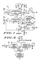
- FIG. l there is shown a simplified block diagram of an integrated speakerphone circuit within dashed outline l0 which incorporates attenuator control circuit l2 of the present invention.
- the speakerphone provides hand free communication in a half-duplex mode operation.
- Half-duplex operation is provided by controlling the gain-attenuation of attenuators l4 and l6 which are respectively situated in transmit and receive signal paths of the speakerphone.
- the speakerphone in a typical application, is coupled to telephone lines at terminals l8 and 20 to provide voice transmission and reception thereover.
- Attenuator control circuit l2 controls the gain of the two attenuators and is voice activated to place the speakerphone in either a transmit or receive mode accordingly.
- the transmit signal path comprises a microphone (not shown) coupled externally at input 22 to audio amplifier 24.
- the output of audio amplifier 24 is connected both to a background level detector 26 and the input of transmit attenuator l4, the output of the latter being connected to output terminal l8.
- the receive signal path includes receive attenuator l6 coupled between terminal 20 and audio amplifier 28.
- a speaker (not shown) is externally connected at terminal 30 to the output of audio amplifier 28.
- a source of operating potential V+ is provided to the speaker phone at terminal 32 and is utilized to derive the power supply voltage V CC for biasing the internal circuitry of the speakerphone.
- the speakerphone is voice switched to be operated in either a transmit mode or receive mode.
- Attenuator control circuit l2 provides a voltage via lead 34 that commonly drives transmit and receive attenuators l4 and l6 accordingly.
- transmitter and receive attenuators l4 and l6 are complimentary in function, i.e., when one is operated at maximum gain the other is operated at maximum attenuation and vice versa.
- Attenuator control circuit l2 The operation of attenuator control circuit l2 is controlled by the three control signals supplied thereto. These signals are, (l) a background level signal XDC supplied via lead 36, (2) a volume level control signal VLC supplied via lead 37, and (3) a control signal applied over lead 38 from T-R comparator 40. Volume control is provided by varying the potentiometer wiper arm of external potentiometer 42 and is connected at terminal 44 to the speakerphone. Thus, by increasing VLC by moving the wiper arm towards V B , a modulated control voltage V is produced at the output of attenuator control circuit l2 via lead 34 to increase the gain of receive attenuator l6 while reducing the relative gain of transmit attenuator l4. The maximum gain/attenuation values of transmit and receive attenuators l4 and l6 are determined respectively by adjusting variable resistors 46 and 48 which are coupled to the attenuators at terminals 50 and 52.
- the speakerphone In addition to operating in a transmit and receive mode, the speakerphone is operated in an idle mode. In the idle mode, no controlling speech signals are coupled to inputs 54 and 56. In this condition the outputs of transmit and receive level detectors 58 and 60, which are coupled respectfully to terminals 54 and 56, cause the output of comparator 40 to be in a high level state. Simultaneously, the voltage at terminal 62 (established across capacitor 64 and resistor 66) is sufficiently low which in conjunction with the output of detector 26 also being in a low level state causes the output of attenuator control circuit l2 to be at a value that reduces the gain of the two attenuators to some midrange value thereof.
- the speakerphone is placed in a transmit mode when there is sufficient transmit signal, such as speech signal, present over and above any receive signal.
- transmit signal such as speech signal
- the relative outputs of transmit and receive level detectors 58 and 60 cause T-R comparator 40 to go to a high output level state.
- background level detector 26 determines whether the transmit signal is a result of background noise or speech. If the signal is due to background noise, the attenuators are placed in the idle mode as described above.
- transmit and receive attenuators l4 and l6 will be switched to a transmit mode by background level detector 26 producing the appropriate control signal at the output of attenuator control circuit l2 to maximize the gain of transmit attenuator l4 while minimizing the gain of receive attenuator l6.
- the speakerphone is placed in the receive mode by the output of attenuator control circuit l2 being switched accordingly when the output of T-R comparator 40 goes low. This occurs whenever there is sufficient receive signal supplied at terminal 20 to overcome any background noise and any speech signals appearing at output l8. In this situation the outputs of transmit and receive level detectors 58 and 60 are such to cause the output of T-R comparator 40 to go to its low level state. Hence, the gain of the receive attenuator l6 is maximized simultaneously with the gain of transmitted attenuator l4 being minimized by the output of attenuator control circuit l2.
- transmit and receive attenuators l4 and l6 may be realized by conventional 2 or 4 quadrant multiplier circuits which are known to those skilled in the art.
- the gains of the attenuators are varied by varying the DC voltage drive supplied thereto accordingly. It is important, that the relative gains of attenuators l4 and l6 do not change over temperature.
- the voltage which drives these multipliers must have a voltage temperature characteristics that varies in the same manner as that of the multipliers themselves.
- Attenuator control circuit l2 of the present invention provides such a voltage as will be hereinafter explained.
- Thermal current reference 70 produces a current I having a predetermined temperature coefficient.
- the current I flows through either receive volume control circuit 74 or transmit gain control circuit 80 depending upon the state of electronic switch 72.
- receive voltage control circuit 74 in response to the output of T-R comparator 40 being low, the current I flows through receive voltage control circuit 74 to develop the corresponding voltage V across resistor 76 which is proportional to absolute temperature.
- the voltage at node 78 that appears over lead 34 to drive transmit and receive attenuators l4 and l6 has the same voltage-temperature characteristics as the attenuators.
- switch 72 In response to the speakerphone being in a transmit mode, switch 72 renders receive volume control circuit 74 nonoperative while transmit gain control circuit 80 is rendered operative to permit the current I to flow through the latter.
- the signal appearing on lead 36 is high such that none of the current I is steered to node 78, to flow through resistor 76.
- resistor 76 In the transmit mode the signal appearing on lead 36 is high such that none of the current I is steered to node 78, to flow through resistor 76.
- the voltage V developed is equal to zero.
- the current I flows through transmit gain control circuit 80 as during the transmit mode. However, in this event a current is steered to node 78 to produce a voltage drop across resistor 76 that is proportional to the value of the voltage appearing at node 62 produced across resistor 66 and capacitor 64.
- the voltage drop across resistor 76 in the idle mode is also proportional to absolute temperature such that the gains of the respective transmit and receive attenuators is not temperature dependent.
- Thermal current source 70 includes PNP transistor 82 interconnected with NPN transistors 84, 86, 88 and 90 to provide the thermal current I at node 92.
- Current source 70 is conventional in structure and the operation thereof is understood by those skilled in the art. Briefly, however, the emitter of transistor 82 is coupled via resistor 94 and 96 to V CC , a source of substantially constant potential having a zero temperature coefficient.
- Transistor 82 is biased on by its base being biased at a potential less than V CC whereby equal currents flow from the two collectors thereof to the respective collectors of NPN transistors 84 and 86.
- Transistor 84 is connected as a diode and forms with transistor 86 a conventional current mirror circuit whereby the current flowing through transistor 86 is substantially equal to the current flowing through the diode connected transistor 84.
- the emitters of transistors 84 and 86 are coupled respectively through resistors 98 and l00 to ground reference.
- area ratioing the effective emitter areas of transistors 84 and 86 the current densities of the two are substantially different. For example, by making the effective area of transistor 84 larger than the effective emitter area of transistor 86 a smaller base to emitter voltage is developed in the former which causes a delta voltage to be developed across resistor 98 which has a positive temperature coefficient.
- This voltage produces a current through resistor 98 which flows through Darlington configured transistors 88 and 90 to node 92.
- This current will also have a positive temperature coefficient due to the fact that it was produced by a positive temperature voltage established across resistor 98.
- Darlington configured transistors 88 and 90 also provide feedback from the collector of transistor 86 to the emitter of transistor 84 to ensure that the two collector currents flowing through transistors 84 and 86 are maintained substantially constant.
- a thermal current I is produced at node 92 which is steered to either receive volume control circuit 74 or transmit gain control circuit 80.
- Transistor l02 which is coupled between receive volume control circuit 74 and transmit gain control circuit 80 to node 92 functions as an electronic switch whereby current is steered to one or the other of the two aforementioned circuits. For example, if the output of T-R comparator 40 is high, thermal current I flows through the current mirror comprising PNP transistors l06 and l08 and resistors ll0 and ll2 as transistor l02 is turned on. In this condition, the voltage developed at the emitter of transistor l02, which is one diode voltage drop below the voltage applied at the base thereof, is sufficient to render receive volume control circuit 74 nonoperative.
- Transmit gain control circuit 80 is now rendered operative whereby the current at node 92 flows through transistor l08 of the current mirror to produce a current through transistor l06 which is substantially equal in magnitude to the current flowing at node 92 and has the same temperature coefficient thereas.
- the current flowing through transistor l06 provides the "tail" current required by the comparator comprising differentially connected transistors ll4 and ll6, the emitters of which are commonly connected to the collector of transistor l06.
- the collector current of transistor l06 is steered proportionally between transistors ll4 and ll6.
- a high level output signal is supplied over lead 36 which will reverse bias PNP transistors ll8 and l20, which are connected in a Darlington configuration and via resistor l22 to the base of transistor ll4. Since these transistors are reverse biased, transistor ll4 is rendered nonconductive as there is no path for base current flow therefrom. Therefore all of the tail current supplied from transistor l06 is steered through transistor ll6 to ground reference through the collector of this transistor. Transistor ll6 is biased in a conducting state since its base is connected at node l24 to which a substantially constant bias potential is established.
- the bias potential is developed through diodes l26 and l28 which are series connected between V CC and the base of transistor ll6. Hence, current flows through the two diodes and via resistor l30 through Darlington configured PNP transistors l32 and l34 to ground reference. Since all of the tail current supplied at the common emitters of transistors ll4 and ll6 of the comparator is steered to ground, in this case one output of the comparator, there is no current flowing through node 78 and resistor 76 (FIG. 2). Thus, transmit attenuator l4 will be operated at maximum gain as previously described with receive attenuator l6 being set at maximum attenuation.
- transmit gain control circuit 80 does not have any control over attenuator control circuit l2.
- the input to the comparator, at the base of transistor ll8, is a function of the voltage XDC. If XDC is less than the voltage established at node l24 transistors ll8, l20 and ll4 are turned on as a path for base current drive is now provided to transistor ll4 through resistor l22. Diode l26 provides current flow therethrough from diode l36 through resistor l22. As transistor ll4 is turned on one-half of the tail current supplied by transistor l06 is steered through the current mirror comprising NPN transistors l38 and l40. Transistor l38 is connected as a diode and has its emitter connected through resistor l42 to ground reference.
- transistor l40 has its base connected to the collector-base of transistor l38 and its emitter coupled through resistor l44 to ground.
- the current steered through transistor ll4 is mirrored at the collector of transistor l40 such that this current now flows through node 78 and resistor 76 to produce the modulated voltage V thereacross.
- the current flowing through node 78 has substantially the same temperature coefficient as the current produced by thermal current reference source 70.
- the magnitude of current steered at the output of the comparator (the collector of transistor l40) is a function of magnitude of the voltage VXDC.
- receive volume control circuit 74 includes a differential amplifier circuit comprising NPN transistors l46 and l48 the emitters of which are commonly connected via resistors l50 and l52.
- a source of tail current is supplied to this differential amplifier at the interconnection of the two resistors by transistor l54 which has its collector emitter path coupled therebetween to ground.
- the base of transistor l54 is biased at a bias potential that is developed across diode l56.
- the bias current in diode l56 will have a zero temperature coefficient since the current through the diode is provided by transistor l58 via resistor 96 which are series coupled between V CC and the diode assuming that the current through resistor 94 is negligibly small in comparison to the current flow through resistor 96.
- the current through resistor 96, transistor l58 and diode l56 also has a zero temperature coefficient.
- the base of transistor l58 is connected with the base of PNP transistor 82 to the interconnection between the emitter of transistor l60 and resistor l62, the other side of which is connected to ground reference.
- the voltage resistor divider comprising resistor l64 and l66 connected between V CC and ground reference produces the potential, V B , which is supplied at the base of transistor l60 and is substantially constant having a zero temperature coefficient.
- the base of transistor l46 is also connected to V B with the base of transistor l48 being connected at terminal 44 to the potentiometer 42.
- the external bias voltage VLC applied to the base of transistor l48, also has a zero temperature coefficient such that the operation of the differential amplifier is independent of temperature.
- the outputs of the differential amplifier (the collectors of transistors l46 and l48) are connected through respective diodes l74 and l76 to V CC through diode l78.
- Receive volume control circuit 74 also includes differential amplifier l68 formed by NPN transistors l70 and l72 the emitters of which are commonly connected to node 92 to thermal current reference source 70. The base electrodes of these two transistors are connected respectively to the collectors of transistors l46 and l48. The outputs of the differential amplifier are taken at the collectors of transistors l70 and l72 with the former being connected to node 78 to resistor 76 and the latter being connected to V CC .
- the current I appearing at node 92 is steered to the common emitters of transistors of l70 and l72 of differential amplifier l68.
- VLC the magnitude of the current flowing through transistor l70 can be varied with respect to the current flowing through transistor l72. For example, as VLC is increased, diode l76 is turned on harder to supply more collector current to transistor l48 which, in turn, causes transistor l72 to be rendered less conductive.
- the speakerphone is therefore operated in a receive mode whenever transistor l02 is turned off. Also, by varying VLC the volume of the receive signal path is increased as the voltage drive signal produced at node 78 and via lead 34 to transmit and receive attenuators l4 and l6 decreases which increases the gain of receive attenuator l6 while increasing the attenuation of the transmit attenuator l4.
- control circuit for producing a voltage drive signal that is proportional to absolute temperature.
- the control circuit can be used in many applications including controlling the gain/attenuation of the receive and transmit signal paths of a half-duplex operated speaker phone system.
Landscapes
- Engineering & Computer Science (AREA)
- Multimedia (AREA)
- Signal Processing (AREA)
- Physics & Mathematics (AREA)
- General Physics & Mathematics (AREA)
- Automation & Control Theory (AREA)
- Amplifiers (AREA)
- Control Of Amplification And Gain Control (AREA)
- Transceivers (AREA)
- Networks Using Active Elements (AREA)
Applications Claiming Priority (2)
| Application Number | Priority Date | Filing Date | Title |
|---|---|---|---|
| US06/772,482 US4689506A (en) | 1985-09-04 | 1985-09-04 | Control circuit for use with electronic attenuators and method for providing a control signal proportional to absolute temperature |
| US772482 | 1985-09-04 |
Publications (3)
| Publication Number | Publication Date |
|---|---|
| EP0214472A2 true EP0214472A2 (fr) | 1987-03-18 |
| EP0214472A3 EP0214472A3 (en) | 1988-07-20 |
| EP0214472B1 EP0214472B1 (fr) | 1991-12-27 |
Family
ID=25095211
Family Applications (1)
| Application Number | Title | Priority Date | Filing Date |
|---|---|---|---|
| EP86110924A Expired - Lifetime EP0214472B1 (fr) | 1985-09-04 | 1986-08-07 | Circuit de commande à utiliser avec des atténuateurs électroniques et méthode pour produire un signal de commande proportionnel à la température absolue |
Country Status (7)
| Country | Link |
|---|---|
| US (1) | US4689506A (fr) |
| EP (1) | EP0214472B1 (fr) |
| JP (1) | JPS6259407A (fr) |
| KR (1) | KR910000688B1 (fr) |
| DE (1) | DE3683105D1 (fr) |
| HK (1) | HK5194A (fr) |
| SG (1) | SG141893G (fr) |
Cited By (1)
| Publication number | Priority date | Publication date | Assignee | Title |
|---|---|---|---|---|
| FR2613157A1 (fr) * | 1987-03-27 | 1988-09-30 | Mennecier Philippe | Dispositif d'interphonie radio miniature et individuel permettant le dialogue simultane de plusieurs utilisateurs |
Families Citing this family (2)
| Publication number | Priority date | Publication date | Assignee | Title |
|---|---|---|---|---|
| US7221659B1 (en) * | 2001-12-31 | 2007-05-22 | Cisco Technology, Inc. | Method and system for managing erroneous attenuation of signal |
| CA2549736A1 (fr) * | 2003-12-05 | 2005-06-23 | The University Of North Carolina At Chapel Hill | Benzofuranes substitues cationiques utiles en tant qu'agents antimicrobiens |
Family Cites Families (9)
| Publication number | Priority date | Publication date | Assignee | Title |
|---|---|---|---|---|
| FR2500698B1 (fr) * | 1981-02-20 | 1989-02-17 | Thomson Csf Mat Tel | Dispositif anti-effet larsen pour poste telephonique |
| DE3148202A1 (de) * | 1981-12-05 | 1983-06-09 | Licentia Patent-Verwaltungs-GmbH, 60325 Frankfurt | "schaltungsanordnung zur gegensinnigen verstaerkungssteuerung von verstaerkern" |
| FR2518854B1 (fr) * | 1981-12-18 | 1986-08-08 | Thomson Csf Mat Tel | Poste telephonique a amplificateurs de parole |
| JPS5979617A (ja) * | 1982-10-27 | 1984-05-08 | Mitsubishi Electric Corp | 可変利得増幅器の制御回路 |
| US4490582A (en) * | 1983-02-18 | 1984-12-25 | At&T Information Systems Inc. | Speakerphone control circuit |
| NL8301138A (nl) * | 1983-03-31 | 1984-10-16 | Philips Nv | Stroombronschakeling. |
| US4591743A (en) * | 1983-12-19 | 1986-05-27 | National Semiconductor Corporation | Temperature compensated current sensing circuit |
| JPS60134548A (ja) * | 1983-12-22 | 1985-07-17 | Fujitsu Ltd | 拡声電話装置 |
| US4593208A (en) * | 1984-03-28 | 1986-06-03 | National Semiconductor Corporation | CMOS voltage and current reference circuit |
-
1985
- 1985-09-04 US US06/772,482 patent/US4689506A/en not_active Expired - Fee Related
-
1986
- 1986-08-07 EP EP86110924A patent/EP0214472B1/fr not_active Expired - Lifetime
- 1986-08-07 DE DE8686110924T patent/DE3683105D1/de not_active Expired - Lifetime
- 1986-08-20 KR KR1019860006862A patent/KR910000688B1/ko not_active Expired
- 1986-09-04 JP JP61208842A patent/JPS6259407A/ja not_active Expired - Lifetime
-
1993
- 1993-12-31 SG SG141893A patent/SG141893G/en unknown
-
1994
- 1994-01-20 HK HK51/94A patent/HK5194A/en not_active IP Right Cessation
Cited By (1)
| Publication number | Priority date | Publication date | Assignee | Title |
|---|---|---|---|---|
| FR2613157A1 (fr) * | 1987-03-27 | 1988-09-30 | Mennecier Philippe | Dispositif d'interphonie radio miniature et individuel permettant le dialogue simultane de plusieurs utilisateurs |
Also Published As
| Publication number | Publication date |
|---|---|
| KR910000688B1 (ko) | 1991-01-31 |
| EP0214472B1 (fr) | 1991-12-27 |
| KR870003414A (ko) | 1987-04-17 |
| JPS6259407A (ja) | 1987-03-16 |
| HK5194A (en) | 1994-01-28 |
| US4689506A (en) | 1987-08-25 |
| DE3683105D1 (de) | 1992-02-06 |
| EP0214472A3 (en) | 1988-07-20 |
| SG141893G (en) | 1994-03-31 |
Similar Documents
| Publication | Publication Date | Title |
|---|---|---|
| US4431874A (en) | Balanced current multiplier circuit for a subscriber loop interface circuit | |
| US4002852A (en) | Electronic telephone network | |
| WO1992012588A1 (fr) | Circuit d'amplificateur adaptable | |
| US4464632A (en) | Volume control circuit | |
| US4143247A (en) | Automatic signal level adjusting circuits for use in telephone sets | |
| US4453038A (en) | Circuit arrangement for producing control means from line current | |
| CA1257724A (fr) | Circuits telephoniques | |
| US4491800A (en) | Switching circuit operable as an amplifier and a muting circuit | |
| EP0225332B1 (fr) | Circuit equilibre a reactance variable et procede de production | |
| US4567384A (en) | Voltage offset producing circuit for use with a line receiver or the like | |
| EP0214472B1 (fr) | Circuit de commande à utiliser avec des atténuateurs électroniques et méthode pour produire un signal de commande proportionnel à la température absolue | |
| KR910004058B1 (ko) | 확성 전화기 | |
| US4432097A (en) | Tone control circuit | |
| US4485341A (en) | Current limiter circuit | |
| JPH0525201B2 (fr) | ||
| JPS6135058A (ja) | 電流特性整形回路 | |
| CA1134522A (fr) | Commutateur vocal pour appareil de communication laissant les mains libres | |
| US4723280A (en) | Constant current line circuit | |
| US4723278A (en) | Voice circuit of telephone | |
| US4856058A (en) | Office line interface circuits | |
| US4405903A (en) | Variolosser for an automatic gain control circuit | |
| US4031331A (en) | Telephone speech network | |
| US4006427A (en) | Automatic gain control circuit | |
| CA1072698A (fr) | Reseau telephonique electronique | |
| CA1268826A (fr) | Amplificateur de sortie |
Legal Events
| Date | Code | Title | Description |
|---|---|---|---|
| PUAI | Public reference made under article 153(3) epc to a published international application that has entered the european phase |
Free format text: ORIGINAL CODE: 0009012 |
|
| AK | Designated contracting states |
Kind code of ref document: A2 Designated state(s): DE FR GB IT NL SE |
|
| PUAL | Search report despatched |
Free format text: ORIGINAL CODE: 0009013 |
|
| AK | Designated contracting states |
Kind code of ref document: A3 Designated state(s): DE FR GB IT NL SE |
|
| 17P | Request for examination filed |
Effective date: 19880929 |
|
| 17Q | First examination report despatched |
Effective date: 19900507 |
|
| GRAA | (expected) grant |
Free format text: ORIGINAL CODE: 0009210 |
|
| AK | Designated contracting states |
Kind code of ref document: B1 Designated state(s): DE FR GB IT NL SE |
|
| ITF | It: translation for a ep patent filed | ||
| REF | Corresponds to: |
Ref document number: 3683105 Country of ref document: DE Date of ref document: 19920206 |
|
| ET | Fr: translation filed | ||
| PLBE | No opposition filed within time limit |
Free format text: ORIGINAL CODE: 0009261 |
|
| STAA | Information on the status of an ep patent application or granted ep patent |
Free format text: STATUS: NO OPPOSITION FILED WITHIN TIME LIMIT |
|
| 26N | No opposition filed | ||
| EAL | Se: european patent in force in sweden |
Ref document number: 86110924.7 |
|
| REG | Reference to a national code |
Ref country code: GB Ref legal event code: 746 Effective date: 19990706 |
|
| PGFP | Annual fee paid to national office [announced via postgrant information from national office to epo] |
Ref country code: NL Payment date: 20000620 Year of fee payment: 15 |
|
| PGFP | Annual fee paid to national office [announced via postgrant information from national office to epo] |
Ref country code: GB Payment date: 20000703 Year of fee payment: 15 |
|
| PGFP | Annual fee paid to national office [announced via postgrant information from national office to epo] |
Ref country code: DE Payment date: 20000720 Year of fee payment: 15 |
|
| PGFP | Annual fee paid to national office [announced via postgrant information from national office to epo] |
Ref country code: SE Payment date: 20000802 Year of fee payment: 15 |
|
| PGFP | Annual fee paid to national office [announced via postgrant information from national office to epo] |
Ref country code: FR Payment date: 20000803 Year of fee payment: 15 |
|
| PG25 | Lapsed in a contracting state [announced via postgrant information from national office to epo] |
Ref country code: GB Free format text: LAPSE BECAUSE OF NON-PAYMENT OF DUE FEES Effective date: 20010807 |
|
| PG25 | Lapsed in a contracting state [announced via postgrant information from national office to epo] |
Ref country code: SE Free format text: LAPSE BECAUSE OF NON-PAYMENT OF DUE FEES Effective date: 20010808 |
|
| PG25 | Lapsed in a contracting state [announced via postgrant information from national office to epo] |
Ref country code: NL Free format text: LAPSE BECAUSE OF NON-PAYMENT OF DUE FEES Effective date: 20020301 |
|
| GBPC | Gb: european patent ceased through non-payment of renewal fee |
Effective date: 20010807 |
|
| EUG | Se: european patent has lapsed |
Ref document number: 86110924.7 |
|
| PG25 | Lapsed in a contracting state [announced via postgrant information from national office to epo] |
Ref country code: FR Free format text: LAPSE BECAUSE OF NON-PAYMENT OF DUE FEES Effective date: 20020430 |
|
| NLV4 | Nl: lapsed or anulled due to non-payment of the annual fee |
Effective date: 20020301 |
|
| PG25 | Lapsed in a contracting state [announced via postgrant information from national office to epo] |
Ref country code: DE Free format text: LAPSE BECAUSE OF NON-PAYMENT OF DUE FEES Effective date: 20020501 |
|
| REG | Reference to a national code |
Ref country code: FR Ref legal event code: ST |
|
| REG | Reference to a national code |
Ref country code: FR Ref legal event code: D6 |
|
| PG25 | Lapsed in a contracting state [announced via postgrant information from national office to epo] |
Ref country code: IT Free format text: LAPSE BECAUSE OF NON-PAYMENT OF DUE FEES;WARNING: LAPSES OF ITALIAN PATENTS WITH EFFECTIVE DATE BEFORE 2007 MAY HAVE OCCURRED AT ANY TIME BEFORE 2007. THE CORRECT EFFECTIVE DATE MAY BE DIFFERENT FROM THE ONE RECORDED. Effective date: 20050807 |