EP0214541A2 - Dispositif pour la mise sous forme numérique d'un signal analogique - Google Patents
Dispositif pour la mise sous forme numérique d'un signal analogique Download PDFInfo
- Publication number
- EP0214541A2 EP0214541A2 EP86111712A EP86111712A EP0214541A2 EP 0214541 A2 EP0214541 A2 EP 0214541A2 EP 86111712 A EP86111712 A EP 86111712A EP 86111712 A EP86111712 A EP 86111712A EP 0214541 A2 EP0214541 A2 EP 0214541A2
- Authority
- EP
- European Patent Office
- Prior art keywords
- filter
- frequency
- analog
- sample
- line
- Prior art date
- Legal status (The legal status is an assumption and is not a legal conclusion. Google has not performed a legal analysis and makes no representation as to the accuracy of the status listed.)
- Withdrawn
Links
Images

Classifications
-
- G—PHYSICS
- G11—INFORMATION STORAGE
- G11C—STATIC STORES
- G11C27/00—Electric analogue stores, e.g. for storing instantaneous values
- G11C27/02—Sample-and-hold arrangements
- G11C27/024—Sample-and-hold arrangements using a capacitive memory element
- G11C27/026—Sample-and-hold arrangements using a capacitive memory element associated with an amplifier
Definitions
- the invention relates to a device for digitizing an analog signal, with a band limiting filter, a sample and hold element and with an analog / digital converter.
- Generally known devices of the type mentioned consist of a series circuit of a band limit filter, a sample and hold element (sample and hold) and an analog / digital converter.
- the band limiting filter ensures that no high-frequency signal parts are passed through, the frequency of which is greater than half the sampling frequency.
- the sample and hold element forms the individual sample values from the analog signal and stores them for the time of a sampling interval.
- the analog / digital converter quantizes the individual samples according to a given rule, so that they appear in the form of a data word.
- the invention as characterized by the claims solves the problem of creating a device, the structure of which is simplified compared to known devices, without adversely affecting their functioning.
- the advantages achieved by the invention can be seen in particular in the fact that a sample and hold element, as is usually connected upstream of an analog / digital converter, can be saved.
- the filter and the sample and hold element are integrated together using the same elements, so that an independent sample and hold element no longer occurs.
- the filter's output driver will converted into a sample and hold element by adding a switch and a capacitor as used in the filter.
- the filter function can additionally be changed and adapted by a computer, and also continuously, by the computer outputting a signal.
- the filter function can be changed in a certain range without having to replace components of the filter. In this way, the signal processing can be continuously optimally adapted to the incoming signals.
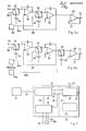
- the block diagram as shown in FIG. 1 is intended for a device which is designed for processing physiological measurement signals, such as can be tapped, for example, in the vicinity of the heart of a living being. Therefore electrodes 1, 2, 3, 4 and 5 are connected to an input amplifier group 11 via lines 6, 7, 8, 9 and 10. Such input amplifier groups are known per se and serve to form so-called derivatives or differences between the signals from two electrodes each.
- the input amplifier group 11 consists of a signal difference formation circuit 11a and amplifiers 11b connected to it.
- Lines 12, 13 and 14 connect the input amplifier group 11 each with a band limiting filter 15, 16 and 17. Via lines 18, 19 and 20, the band limiting filters 15, 16 and 17 are each connected to an analog / digital valley converter 21, 22 and 23 connected.
- Lines 24, 25 and 26 in turn connect them to a multiplexer 27, which in turn is connected to a computer 29 via lines 28.
- the computer 29 has a bus 30 as an output.
- a timing controller 31 is provided as the clock signal source. It can be understood as part of the computer 29.
- the computer 29 is connected to an input unit 33 via a bus 32.
- a quartz 34 is connected to the computer 29 via a line 35.
- Lines 36, 37, 38 and 38a are provided for the transmission of clock signals from the time controller 31 to the band limitation filters 15, 16 and 17, to the analog / digital converters 21, 22 and 23 and to the multiplexer 27.
- a high-pass filter 39 can also be connected between the band limitation filters 15, 16, 17 and the analog / digital converters 21, 22, 23. It is used to switch off a DC voltage component of the signals.
- Figure 2a shows an example of a filter with sampling of analog input values according to the prior art. It is designed as a known second-order SC filter with a low-pass characteristic. It each has an input 40 and an output 41 and capacitors 44 and 45 connected via switches 42 and 43. Switches 42 and 43 are preferably implemented in semiconductor technology. The switches 42 and 43 are each followed by an integrator 46 and 47, which are also connected to one another via a feedback 48. The integrators 46 and 47 are followed by an operational amplifier 50 with a feedback 51 to its inverting input, which serves to amplify the signals of the last integrator 4 7 to such an extent that they can be used for the subsequent signal processing.
- This operational amplifier 50 with its feedback 51 has the function of a buffer as is generally provided in such filters in an integrated design and is also referred to as an output driver.
- the switch 42 is connected to the line 36.
- the switch 43 is connected to the line 36 via a delay element 49 and a line 36a sen.
- the delay element 49 causes the delay signals from line 36 to be delayed by a fraction of a clock period.
- FIG. 2b shows essentially exactly the same filter with sampling of analog input values with two filter stages 42, 44, 46 and 43, 45, 47 as shown in FIG. 2a.
- a switching element 52 with a capacitor 53 as a capacitance is connected upstream of the operational amplifier 50.
- the switching element 52 and the capacitance 53 are identical to the switches 42 and 43 and their capacitors 44 and 45 of the filter stages.
- the switching element 52 is also connected via lines 36b and possibly also a further delay unit 49b to the line 36, which supplies it with the clock frequency. Switching element 52 can also be connected directly to line 36a or to line 37.
- FIG. 3 again shows schematically the quartz 34 which is connected to the computer 29 via a line 35.
- the computer 29 has a generator 61 and a frequency divider 62. Lines 36, 37, 38 and 38a form outputs from the frequency divider 62.
- the generator 61 and the frequency divider 62 together form the time control or clock frequency source 31.
- the generator 61 is connected to the frequency divider 62 via a line 63 and to the line 64 via further lines 64
- Microprocessor 60 connected.
- a line 65 connects this to the frequency divider 62.
- the bus 32 is connected to the microprocessor 60.
- the microprocessor 60 is also connected via a bus 67 to a memory 66, which is preferably designed as RAM.
- the microprocessor 60 is connected to the line 28, so that all the samples can be fed to it.
- the quartz 34 emits a very high-frequency oscillation in the megahertz range to the generator 61 via the line 35. This converts this sinusoidal oscillation into a sequence of rectangular pulses which are fed to the frequency divider 62 via the line 63.
- the frequency divided by 2 ' is output via line 36.
- the frequency divided by 2 1 is output via line 37.
- the frequencies of the clock signals in lines 36 and 37 differ by a factor of k. Additional clock signals with other frequencies can be emitted via lines 38 and 38a.
- the microprocessor 60 can output the values for the factors k, 1 and i to the frequency divider 62 via the line 65. Via the lines 64, the generator 61 also outputs clock signals to the microprocessor 60, which needs them for its work. The generator 61 likewise receives 64 start and stop signals via this line.
- the electrodes 1, 2, 3, 4 and 5 deliver analog signals, for example in the form of electrical voltages.
- signal differences are formed from the signals of two of the lines 6, 7, 8, 9 or 10, which are then amplified in the amplifier 11b.
- the lines 12, 13 and 14 are analog signals, which are freed in the bandpass filters 15, 16 and 1 7 from possible high frequency signal components to later their Rueckfaltung to avoid, in the frequency range of the lower-frequency useful signals, as in the digitization of signals is known as "aliasing".
- band limiting filters can be designed as passive filters (consisting of resistors, capacitors and inductors) but also as active filters (with operational amplifiers instead of inductors).
- band limitation filters as filters with sampling of analog input values.
- the analog input values are first sampled with a certain sampling frequency.
- the sample values thus obtained are then further processed so that the desired filter function for the integrated output samples of the filter is fulfilled.
- filters are the filters with switched capacitances (also known as SC filters).
- SC filters also known as SC filters.
- the resistors are replaced by capacitances that can be switched on and off by switching elements.
- An example of such a filter is the type MF6CN from National Semiconductors.
- the use of independent scanning and holding elements downstream of the filter can be dispensed with. This is because the function of such filters is to break down the incoming analog signal into a sequence of samples. However, this with a frequency that does not correspond to the sampling frequency desired for the device, but is determined by the frequency response that the filter should have.
- the switching element 52 In order to obtain sample values at the output 41 with the sampling frequency for the analog / digital converter or with a multiple of this sampling frequency, the switching element 52 (FIG. 2b) must be driven with an appropriate frequency. This frequency can be a multiple of the sampling frequency, but must not exceed the filter frequency.
- the downstream analog / digital converter then only records values with the sampling frequency, even if values with a higher frequency are obtained.
- band limiting filters are usually designed as low-pass filters. Above an upper limit frequency, they block the passage for signals or signal parts with a higher frequency. According to Shannon's sampling theorem, the sampling frequency for the digitization of such signals must be at least twice as high as this upper limit frequency. However, for the MF6CN filter mentioned, the frequency with which the analog input values are sampled is at least fifty times higher than the upper limit frequency of the filter or at least twenty-five times higher than the sampling frequency that is desired for digitization.
- the entire device according to FIG. 1 is controlled by clock signals from the quartz 34.
- the timing controller 31 can derive from these clock signals for the individual elements other clock signals whose frequency is in a fixed ratio to the clock signals from the quartz 34.
- a high-frequency clock signal is fed, for example, via line 36 to the band limiting filters 15, 16 and 17.
- the switching elements 42, 43 in the SC filters (FIG. 2) are actuated by this clock signal and the capacitors 44, 45 are thus periodically charged and discharged again. This happens for example with a frequency of 12.5 kHz. Sampling values thus arise, which are integrated again in the operational amplifier 47, which works as an integrator.
- This signal is sampled again in the switching element 52 and amplified in the operational amplifier 50 in such a way that sample values that are useful for the subsequent signal processing are available.
- the multiplexer 27 collects the digitized samples, which are now expressed by data words of a certain word length, and feeds them to the computer 29. For example, the latter is able to take one of these samples to calculate racumlichen signal course.
- the multiplexer 27 is controlled in a known manner by clock signals from the lines 38 and 38a. However, these clock signals in turn have a higher frequency.
- the clock frequency in line 38 preferably corresponds to the sampling frequency multiplied by the number of lines which the multiplexer 27 has as inputs.
- the clock frequency in line 38a differs by a factor 2/3 from the clock frequency in line 38, for three lines which end in the multiplexer 27. With the two clock signals from lines 38 and 38a, the multiplexer 27 can carry out its work in a known manner.
- Components of the type 63B03 for the computer 29, the type ADC1001 for the analog / digital converters 21, 22 and 23, the type CD 4051 for the multiplexer 27, the type TL064 for the signal difference circuit 11a and the type can be used to implement such a device TL064 can be used for the amplifier 11b.
Landscapes
- Analogue/Digital Conversion (AREA)
- Filters That Use Time-Delay Elements (AREA)
- Networks Using Active Elements (AREA)
Applications Claiming Priority (2)
| Application Number | Priority Date | Filing Date | Title |
|---|---|---|---|
| CH387685 | 1985-09-09 | ||
| CH3876/85 | 1985-09-09 |
Publications (2)
| Publication Number | Publication Date |
|---|---|
| EP0214541A2 true EP0214541A2 (fr) | 1987-03-18 |
| EP0214541A3 EP0214541A3 (fr) | 1988-09-28 |
Family
ID=4265383
Family Applications (1)
| Application Number | Title | Priority Date | Filing Date |
|---|---|---|---|
| EP86111712A Withdrawn EP0214541A3 (fr) | 1985-09-09 | 1986-08-23 | Dispositif pour la mise sous forme numérique d'un signal analogique |
Country Status (2)
| Country | Link |
|---|---|
| EP (1) | EP0214541A3 (fr) |
| JP (1) | JPS6260316A (fr) |
Cited By (1)
| Publication number | Priority date | Publication date | Assignee | Title |
|---|---|---|---|---|
| EP0377965A3 (fr) * | 1989-01-13 | 1991-08-07 | Delco Electronics Corporation | Circuit combiné de désaccentuation et d'élimination de bruit |
Families Citing this family (2)
| Publication number | Priority date | Publication date | Assignee | Title |
|---|---|---|---|---|
| US5099239A (en) * | 1989-09-21 | 1992-03-24 | Xerox Corporation | Multi-channel analogue to digital convertor |
| JP5318053B2 (ja) * | 2010-09-14 | 2013-10-16 | 本田技研工業株式会社 | Ad変換システム |
Family Cites Families (2)
| Publication number | Priority date | Publication date | Assignee | Title |
|---|---|---|---|---|
| JPS55166324A (en) * | 1979-06-14 | 1980-12-25 | Fujitsu Ltd | Switched capacitor filter |
| JPS60154400A (ja) * | 1984-01-23 | 1985-08-14 | Sony Corp | サンプリング回路 |
-
1986
- 1986-08-23 EP EP86111712A patent/EP0214541A3/fr not_active Withdrawn
- 1986-09-09 JP JP21251186A patent/JPS6260316A/ja active Pending
Cited By (1)
| Publication number | Priority date | Publication date | Assignee | Title |
|---|---|---|---|---|
| EP0377965A3 (fr) * | 1989-01-13 | 1991-08-07 | Delco Electronics Corporation | Circuit combiné de désaccentuation et d'élimination de bruit |
Also Published As
| Publication number | Publication date |
|---|---|
| JPS6260316A (ja) | 1987-03-17 |
| EP0214541A3 (fr) | 1988-09-28 |
Similar Documents
| Publication | Publication Date | Title |
|---|---|---|
| EP0052847B1 (fr) | Procédé et circuit pour la conversion de la fréquence d'échantillonnage d'une suite d'échantillons en évitant la conversion en un signal continu | |
| DE3640672C2 (fr) | ||
| DE69014414T2 (de) | Abtast- und Halteanordnung. | |
| DE4331880C2 (de) | CMOS-Spitzenamplitudendetektor | |
| DE69422650T2 (de) | Als dreistufiges transversales Filter anwendbare digitale Filterschaltung | |
| EP0042116B1 (fr) | Circuit de filtre électrique pour le traitement de signaux analogiques d'échantillonnage | |
| DE3133684C2 (de) | Elektronische analoge Schaltvorrichtung | |
| DE2017285A1 (de) | Sperrfilter mit einer Anzahl von nwahlbar anschaltbaren parallelen kapazi tiven Zweigen | |
| DE3001969C2 (de) | Elektrische Filterschaltung unter Verwendung von wenigstens einer simulierten Induktivität, die gesteuerte Schalter, Kondensatoren und Verstärker enthält | |
| DE3137943C2 (fr) | ||
| WO1980000644A1 (fr) | Filtre pour oscillations electriques constitue de commutateurs, de condensateurs et d'amplificateurs | |
| EP0214541A2 (fr) | Dispositif pour la mise sous forme numérique d'un signal analogique | |
| DE2856955C2 (de) | Verfahren und Vorrichtung zur Digital-Analog- und Analog-Digital-Umwandlung | |
| DE602004009766T2 (de) | Gleichstrom-gleichstrom-schaltwandlereinrichtung | |
| DE69128986T2 (de) | Spannungsvergleichsschaltung mit Abtast-Halte-Schaltungsanordnung und deren Benutzung in einem Analog-Digital-Wandler | |
| DE4321621C1 (de) | Schaltungsanordnung zur Signalverarbeitung | |
| DE3015806C2 (de) | Schaltungsanordnung zur Abnahme von Signalen von Halbleiter-Bild- oder -Zeilensensoren | |
| DE69113414T2 (de) | Integrierte Konstantstromversorgung. | |
| DE3855571T2 (de) | Verstärkungsregelungsanlage | |
| DE3885723T2 (de) | Integriertes aktives Tiefpassfilter ersten Grades. | |
| EP0104578B1 (fr) | Convertisseur numérique-analogique avec découplage de potentiel | |
| EP0583490B1 (fr) | Procédé de traitement d'un signal électrique, en particulier un signal dérivé du coeur | |
| DE69516624T2 (de) | Multiplikationsschaltung | |
| DE2933643C2 (de) | Abtastintegrator mit elektronischen Schaltern, insbesondere zur Realisierung getakteter aktiver Filterschaltungen | |
| DE10117384A1 (de) | Sensorvorrichtung |
Legal Events
| Date | Code | Title | Description |
|---|---|---|---|
| PUAI | Public reference made under article 153(3) epc to a published international application that has entered the european phase |
Free format text: ORIGINAL CODE: 0009012 |
|
| AK | Designated contracting states |
Kind code of ref document: A2 Designated state(s): AT BE CH DE FR GB IT LI NL SE |
|
| PUAL | Search report despatched |
Free format text: ORIGINAL CODE: 0009013 |
|
| AK | Designated contracting states |
Kind code of ref document: A3 Designated state(s): AT BE CH DE FR GB IT LI NL SE |
|
| STAA | Information on the status of an ep patent application or granted ep patent |
Free format text: STATUS: THE APPLICATION IS DEEMED TO BE WITHDRAWN |
|
| 18D | Application deemed to be withdrawn |
Effective date: 19890301 |
|
| RIN1 | Information on inventor provided before grant (corrected) |
Inventor name: SCHMID, JOHANN JAKOB Inventor name: THIE, WERNER |