EP0214607A2 - Appareil de prise de vues, par préférence, thermiques - Google Patents
Appareil de prise de vues, par préférence, thermiques Download PDFInfo
- Publication number
- EP0214607A2 EP0214607A2 EP86112163A EP86112163A EP0214607A2 EP 0214607 A2 EP0214607 A2 EP 0214607A2 EP 86112163 A EP86112163 A EP 86112163A EP 86112163 A EP86112163 A EP 86112163A EP 0214607 A2 EP0214607 A2 EP 0214607A2
- Authority
- EP
- European Patent Office
- Prior art keywords
- scanning
- light
- mirror
- scanning mirror
- image
- Prior art date
- Legal status (The legal status is an assumption and is not a legal conclusion. Google has not performed a legal analysis and makes no representation as to the accuracy of the status listed.)
- Granted
Links
Images


Classifications
-
- H—ELECTRICITY
- H04—ELECTRIC COMMUNICATION TECHNIQUE
- H04N—PICTORIAL COMMUNICATION, e.g. TELEVISION
- H04N23/00—Cameras or camera modules comprising electronic image sensors; Control thereof
- H04N23/20—Cameras or camera modules comprising electronic image sensors; Control thereof for generating image signals from infrared radiation only
Definitions
- the present invention relates to a device for generating an image of a scene, preferably a thermal image, according to the preamble of claim 1.
- Such a device is known for example from GB-PS 1 435 144; it is used there as a thermal imaging device.
- the thermal image is scanned bidirectionally, i.e. both when the scanning mirror moves back and forth. This can be pivoted about two axes and is controlled in such a way that the Warrre image is scanned line by line, successive lines being spatially spaced perpendicular to the line direction.
- the known device works according to the so-called double interlacing, with the scanning mirror at the end point of a scanning movement, e.g. the tip is tipped by a small amount and at the end point of the following scanning movement, e.g. so the return tilts back by this amount.
- This type of scanning improves the resolution in the direction of the detector row, for example 240 scanning lines are achieved with 120 detectors in a row.
- Light-emitting elements which, like the detectors, are arranged in series are used to generate the visible image.
- Each individual detector of the row detector is assigned to a light-emitting element via amplifiers.
- a phase shift occurs between the signals generated by the detectors and the signals supplied to the light-emitting elements.
- the light-emitting elements light up with a delay. This would not be a nuisance with unidirectional scanning, but with bidirectional scanning there is a very annoying effect due to the different scanning directions. For example, a bar target would be from the left scanning direction to the right again- following scan line, however, to the left. The Line forming goal was again
- the scanning mirror is arranged in a housing in the thermal imaging device known from GB-PS 1 435 144 t. that can be tilted around an axis that forms an angle of approx. 45 ° with the line scanning axis.
- the housing is fixed with a lens which serves to image the light coming from the light-emitting elements in an image plane. If the housing and thus the mirror are tilted at the end point of a scanning movement, the result is Movement component, which encloses the housing by a small amount pivots. This also pivots the All components are coordinated so that Swiveling the lens around the image in the image plane which shifts that due to the phase shift of the signal Phase error compensated.
- a ere l to apparatus for compensating for the by the Phasenverschie- electrical signal caused phase error is from the 805 531 known. There are for creating the visible image provided by light-emitting elements which are laterally offset relative to one another to compensate for the error to be compensated Return and return of the scanning mirror can be controlled separately.
- the correction element consists of an optical deflection element and electrical means for alternately pivoting this element into two defined positions, is arranged in the beam path between the light-emitting elements and the scanning mirror, and of the line scanning of the signals causing the scanning mirror is controlled.
- the correction element according to the invention is completely mechanically decoupled from the scanning mirror. This makes it possible to arrange and control this element in such a way that the deflection effect exerted by it for the light emitted by the light-emitting elements is only assigned to the scanning directions, and in fact completely independently of the position of the respective scanning line.
- the device according to the invention can be operated with a desired vertical resolution of the generated image without any changes being necessary on the correction element itself.
- the device can thus in particular without interlacing, after the double interlacing or after the quadruple Interlaced.
- the correction element compensates for the phase delay of the electrical signals dissolve effects completely.
- Claim 2 specifies a particularly advantageous embodiment of the invention. This training is simple, works flawlessly and offers no difficulties in assembly and adjustment.
- Claim 5 specifies an embodiment of the device according to the invention, which is distinguished by a good vertical resolution and in which the correction element according to the preceding claims is used in a particularly advantageous manner.
- 1 denotes an input optic which images the thermal radiation coming from the scene via a scanning mirror 2 and a further optic 3 in the plane of a row of detectors 4.
- This row of detectors 4 consists of individual infrared detectors arranged in a row. 1, this row of detectors is arranged perpendicular to the plane of the drawing.
- Each individual detector is connected via a schematically illustrated amplifier chain 5 Element 6 connected, for example as Diode can be formed.
- Such diodes are arranged in a row, which in the illustration in FIG. 1 is again to be considered perpendicular to the plane of the drawing.
- the number of light emitting elements 6 corresponding to the number of individual detectors 4.
- the light emerging from the elements 6, light is via an optical system 7 into a P aralkyl lelstrahlengang converted, which is elenkt from the rear side of the scanning mirror 2 to an image viewing device 8 to q.
- the device 8 can be designed, for example, as an image intensifier or as a telescope.
- the scanning mirror 2 is pivoted about the axis 9 lying parallel to the detector row 4, specifically in the direction of the arrow 10.
- the thermal image is moved in the row direction over the detector row 4, so that each detector in this row has a video signal assigned to an image row generated.
- This video signal controls the brightness of the associated light emitting element 6, i.e. for each scanned pixel, the invisible IR image signal coming from the scene is converted into a visible signal.
- the light emitted by the light-emitting elements 6 is deflected from the rear of the scanning mirror 2, so that the image generated in the image viewing device 8 is independent of any fluctuations in the scanning movement of the mirror 2.
- the scanning mirror 2 can also be tilted about an axis 11 by very small amounts. Such a tilting ensures that the scanning lines traversed during the back and forth movement of the scanning mirror 2 are perpendicular to the line direction, as is required for the interlacing method.
- the work is carried out after double interlacing, i.e. the scanning lines assume 2 different positions in the device shown here during the back and forth movement of the scanning mirror.
- the scanning and the construction of the image are bidirectional, i.e. during the back and forth movement of the scanning mirror 2.
- the signal generated by the passed IR detector 4 essentially corresponds to this course. It is fed to the amplifier chain 5, which has a finite electrical bandwidth.
- the phase shift shown in FIGS. 3b and 3c occurs between the signals generated by the detector 4 and those supplied to the associated light-emitting diode 6. It can be seen that the centers of gravity of the signals shown during the forward (FIG. 3b) and the return (FIG. 3c) of the scanning each shift by an amount ⁇ x relative to the center of gravity of the signal to be actually represented in FIG. 3a. This error is called a phase error.
- the line scan mode is usually used in thermal imaging devices. It is common to use double interlacing, i.e. to double the number of scan lines.
- FIGS. 2 a to e now show different phases of an image scanning according to the four-line interlacing method. Such a procedure has not yet been possible because the means for correcting the phase errors were not available.
- FIG. 2 shows the different scanning phases on the basis of the detectors 40, 41, 42 of the detector row 4 that are selected, for example.
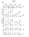
- the corresponding signals used to control the scanning mirror 2 are shown in FIGS. 6a and 6b.
- the scanning mirror 2 is pivoted about the axis 9 and moves the thermal image along the first scanning line 51 via the detectors.
- the scanning mirror 2 is tilted about the axis 11 by supplying the signal U V1 of FIG. 6t>, so that the scanning line 52 is traversed during the following return.
- the position of the previously scanned line is shown in dashed lines in Fig. 2b.
- the scanning mirror 2 becomes white by supplying the signal U V2 tere amount tilted about the axis 11.
- the third scanning line 53 is passed over the detectors.
- 2c shows the position of the previously scanned scanning lines in dashed lines.
- the scanning mirror 2 is tilted by a further angular amount by supplying the signal U V3 and passes through the scanning line 54 of FIG. 2d during the following scanning movement.
- the scanning lines which have previously been run through are shown in dashed lines.
- the mirror 2 is tilted back about the axis 11 by the signal of FIG. 6b, so that the scanning line 55 which was first run through in the subsequent scanning process again corresponds to the scanning line 51.
- the number of scan lines passed is quadrupled. If the detector line 4 contains, for example, 120 individual detectors, 480 scanning lines are run through, i.e. the vertical resolution of the image is significantly improved.
- the scanning mirror 2 is mounted in a mirror frame 12 so as to be pivotable about the axis 9.
- the pivoting of the mirror is effected via a schematically illustrated device 14, which can be designed, for example, as a motor.
- the control device 15 supplies this device with the signal shown in FIG. 6a.
- the mirror frame 12 can be tilted about an axis 11 in a fixed frame 13. This tilting is effected by means of a device 16, which can be designed, for example, as a motor.
- the device 16 is fed, for example, the signal shown in FIG. 6b via the control arrangement 15.
- the radiation emanating from the thermal image is deflected by the scanning mirror 2 onto a row of detectors not visible in FIG. 4.
- the signal coming from this row of detectors is fed via an amplifier chain 5 to the light-emitting diodes 6 arranged in a row.
- the light generated by these diodes is imaged to infinity by a schematically illustrated optic 17 and is directed onto the rear via a deflecting mirror 18. of the scanning mirror 2 thrown. From there, the light reaches the observation device 8 of FIG. 1 that is not visible in this illustration.
- a correction element 20, which serves to correct the phase errors, is arranged in the convergent beam path between the optics 17 and the light-emitting diodes 6.
- This correction element consists of an optical deflection element and electrical means 19 for alternately pivoting this element into two defined positions.
- the arrangement 19 is synchronized via the device 14, which is used to give away the mirror 2 about the axis 9.
- FIG. 5 A very particularly advantageous embodiment of the correction element 20 is shown in FIG. 5.
- 6 denotes a light-emitting diode, which is arranged on a substrate 21.
- the light-emitting diodes are arranged in a row which, in the illustration in FIG. 5, is perpendicular to the plane of the drawing.
- a lens 22 is arranged behind the diode 6 in the beam direction.
- the actual correction element consists of a plane-parallel plate 24 which is arranged on a support 25 so as to be tiltable about an axis 26.
- the carrier 25 is provided with two magnet armatures 27 and 28 which cooperate with the two electromagnets 29 and 30.
- a current is supplied to the electromagnet 29 via the control arrangement 19, the course of which can be seen in FIG. 6d.
- the time course of the current I2 supplied to the electromagnet 30 can be seen from FIG. 6e. It can be seen from this representation that the plane-parallel plate 24 alternately assumes two defined angular positions and in these deflects the light emitted by the light-emitting diodes 6 by an amount ⁇ x (see FIG. 3c).
- An angular position of the plane-parallel plate 24 is in each case assigned to the traverse of the scanning mirror 2, that is, to the deflection signals of FIG. 6a during the times 0 to t 1 and t 2 to t 3 .
- the other angular position of the plane-parallel plate 24 is the return of the deflecting mirror assigned, ie the signal sections of Fig. 6a during the times t 1 to t 2 and t 3 to t 4 '
- This assignment is completely independent of the signals of Fig. 6b, that is, it is completely independent of the tilt of the angle mirror 2 with respect to Axis 11.
- correction element shown and described can be used universally, regardless of whether the thermal imaging device is operated without interlacing, after double interlacing or after quadrupling. Any other interlacing method is also possible without changing the correction element and its control means.
- the correction element of FIG. 5 is advantageously used in a thermal imaging device which is operated according to the quadruple interlace method of FIG. 2. If, in this method, the control device 16 of the deflection mirror 2 is supplied with signals according to FIG. 6b, the scanning takes place as shown in FIG. according to the scheme 1, 2, 3, 4. It is also possible to supply the control device 16 with a signal, the course of which can be seen from FIG. 6c. The scanning then also takes place according to the four-line interlacing method, the scanning scheme now being 1, 3, 2, 4.
- deflection elements can also be used. It is thus possible, for example, to tilt the deflecting mirror 18 of FIG. 4 into two defined angular positions, each of which is assigned to the forward and backward movement of the scanning mirror 2.
- a sliding lens micrometer in the parallel beam path between mirror 2 and optics 17.
- Such a sliding lens micrometer consists of two lenses, one of which is arranged in a fixed manner, while the other takes on two defined displacement positions.
Landscapes
- Engineering & Computer Science (AREA)
- Multimedia (AREA)
- Signal Processing (AREA)
- Transforming Light Signals Into Electric Signals (AREA)
- Mechanical Optical Scanning Systems (AREA)
- Adhesives Or Adhesive Processes (AREA)
- Heat Sensitive Colour Forming Recording (AREA)
Priority Applications (1)
| Application Number | Priority Date | Filing Date | Title |
|---|---|---|---|
| AT86112163T ATE76708T1 (de) | 1985-09-05 | 1986-09-03 | Vorrichtung zur erzeugung eines bildes, einer szene, vorzugsweise eines waermebildes. |
Applications Claiming Priority (2)
| Application Number | Priority Date | Filing Date | Title |
|---|---|---|---|
| DE19853531666 DE3531666A1 (de) | 1985-09-05 | 1985-09-05 | Vorrichtung zur erzeugung eines bildes einer szene, vorzugsweise eines waermebildes |
| DE3531666 | 1985-09-05 |
Publications (3)
| Publication Number | Publication Date |
|---|---|
| EP0214607A2 true EP0214607A2 (fr) | 1987-03-18 |
| EP0214607A3 EP0214607A3 (en) | 1989-03-15 |
| EP0214607B1 EP0214607B1 (fr) | 1992-05-27 |
Family
ID=6280174
Family Applications (1)
| Application Number | Title | Priority Date | Filing Date |
|---|---|---|---|
| EP86112163A Expired - Lifetime EP0214607B1 (fr) | 1985-09-05 | 1986-09-03 | Appareil de prise de vues, par préférence, thermiques |
Country Status (6)
| Country | Link |
|---|---|
| US (1) | US4763001A (fr) |
| EP (1) | EP0214607B1 (fr) |
| AT (1) | ATE76708T1 (fr) |
| CA (1) | CA1260134A (fr) |
| DE (2) | DE3531666A1 (fr) |
| ES (1) | ES2002279A6 (fr) |
Families Citing this family (7)
| Publication number | Priority date | Publication date | Assignee | Title |
|---|---|---|---|---|
| US4988878A (en) * | 1990-03-07 | 1991-01-29 | Associated Universities, Inc. | Support means for a particle beam position monitor |
| FR2691579A1 (fr) * | 1992-05-21 | 1993-11-26 | Commissariat Energie Atomique | Système de conversion d'une image infrarouge en image visible ou proche infrarouge. |
| DE4231401A1 (de) * | 1992-09-19 | 1994-03-24 | Telefunken Microelectron | Bildaufnahmevorrichtung |
| US5481300A (en) * | 1994-04-29 | 1996-01-02 | Motta; Ricardo J. | Image capture system |
| US6069357A (en) * | 1996-09-24 | 2000-05-30 | Alliedsignal Inc. | Dynamic optical scanning correction device |
| JPH11352434A (ja) | 1998-06-08 | 1999-12-24 | Sankyo Seiki Mfg Co Ltd | ビーム走査装置 |
| DE102012009093A1 (de) * | 2012-05-03 | 2013-11-07 | Institut für Photonische Technologien e.V. (IPHT) | Anordnung zur hochdynamischen Abtastung eines Objektfeldes für ein bildgebendes radiometrisches System |
Family Cites Families (10)
| Publication number | Priority date | Publication date | Assignee | Title |
|---|---|---|---|---|
| US3781559A (en) * | 1972-06-19 | 1973-12-25 | Texas Instruments Inc | Variable field of view scanning system |
| US3912927A (en) * | 1972-11-13 | 1975-10-14 | Texas Instruments Inc | Opto-mechanical device for phase shift compensation of oscillating mirror scanners |
| US3949225A (en) * | 1974-09-23 | 1976-04-06 | Xerox Corporation | Infrared imaging apparatus |
| DE2805531C2 (de) * | 1978-02-10 | 1979-08-16 | Fa. Carl Zeiss, 7920 Heidenheim | Verfahren und Vorrichtung zur Erzeugung eines Wärmebildes mit Korn* pensation des Phasenfehlers |
| EP0023108A1 (fr) * | 1979-07-19 | 1981-01-28 | The Marconi Company Limited | Dispositif de balayage optique |
| US4328516A (en) * | 1980-11-17 | 1982-05-04 | The United States Of America As Represented By The Secretary Of The Army | Integral test input for electro-optically multiplexed FLIR system |
| DE3128469C2 (de) * | 1981-07-18 | 1983-09-08 | Eltro GmbH, Gesellschaft für Strahlungstechnik, 6900 Heidelberg | Verfahren und Vorrichtung zum Abtasten von Strahlungsenergie |
| US4520504A (en) * | 1982-07-29 | 1985-05-28 | The United States Of America As Represented By The Secretary Of The Air Force | Infrared system with computerized image display |
| DE3329588C1 (de) * | 1983-08-16 | 1984-10-18 | Eltro GmbH, Gesellschaft für Strahlungstechnik, 6900 Heidelberg | Arbeitsverfahren einer aus Lasersender und Wärmebildgerät kombinierten Geräteanordnung sowie eine Vorrichtung hierzu |
| DE3341066A1 (de) * | 1983-08-16 | 1985-05-23 | Eltro GmbH, Gesellschaft für Strahlungstechnik, 6900 Heidelberg | Waermebildgeraet |
-
1985
- 1985-09-05 DE DE19853531666 patent/DE3531666A1/de active Granted
-
1986
- 1986-09-03 DE DE8686112163T patent/DE3685467D1/de not_active Expired - Fee Related
- 1986-09-03 AT AT86112163T patent/ATE76708T1/de not_active IP Right Cessation
- 1986-09-03 EP EP86112163A patent/EP0214607B1/fr not_active Expired - Lifetime
- 1986-09-04 CA CA000517499A patent/CA1260134A/fr not_active Expired
- 1986-09-04 ES ES8601615A patent/ES2002279A6/es not_active Expired
- 1986-09-05 US US06/904,243 patent/US4763001A/en not_active Expired - Fee Related
Also Published As
| Publication number | Publication date |
|---|---|
| DE3685467D1 (de) | 1992-07-02 |
| DE3531666C2 (fr) | 1993-05-13 |
| ES2002279A6 (es) | 1988-08-01 |
| DE3531666A1 (de) | 1987-03-12 |
| EP0214607B1 (fr) | 1992-05-27 |
| CA1260134A (fr) | 1989-09-26 |
| ATE76708T1 (de) | 1992-06-15 |
| EP0214607A3 (en) | 1989-03-15 |
| US4763001A (en) | 1988-08-09 |
Similar Documents
| Publication | Publication Date | Title |
|---|---|---|
| DE3882359T2 (de) | Abtast-gemultiplexte lichtventildrucker mit streifenverminderndem aufbau. | |
| DE3307745C2 (de) | Rasterelektronenmikroskop | |
| EP3311213B1 (fr) | Procédés de détermination et de compensation des erreurs géométriques d'imagerie | |
| DE10156275B4 (de) | Detektoranordnung und Detektionsverfahren | |
| DE2224275B2 (de) | Vorrichtung zur bilderzeugung mit einer detektoranordnung | |
| DE19704427A1 (de) | Einrichtung zur Regelung der Leuchtweite von Scheinwerfern von Fahrzeugen | |
| DE2332245B2 (de) | Vorrichtung zur Abtastung von Strahlungsenergie | |
| DE69325202T2 (de) | Optische Vermittlungseinrichtung im freien Raum | |
| EP0276337B1 (fr) | Arrangement de diaphragmes pour le balayage optoélectronique des documents | |
| DE3239851A1 (de) | Abtastvorrichtung mit zweidimensionaler radiometrischer kompensation | |
| EP0214607B1 (fr) | Appareil de prise de vues, par préférence, thermiques | |
| DE3320545C3 (de) | Verfahren und Vorrichtung zum Erzeugen eines aus einer Serie von Einzelbildern zusammengesetzten Bildes | |
| EP1198979B1 (fr) | Dispositif d'inspection pour composants | |
| DE3422747A1 (de) | Fernseh-projektionssystem | |
| DE102007025330A1 (de) | Projektionsvorrichtung | |
| EP0003600B1 (fr) | Procédé et dispositif pour produire une image d'une scène, en particulier d'une image thermique à compensation de faute de phase | |
| DE69316724T2 (de) | Head-up Anzeige mit örtlicher Bestimmung des Bildes | |
| DE4103298A1 (de) | Vorrichtung zur abbildung eines objektes | |
| EP3631510B1 (fr) | Dispositif lidar et procédé de balayage d'un angle de balayage au moyen d'au moins un faisceau d'orientation constante | |
| DE3338496C2 (de) | Afokales Wärmebildgerät | |
| WO2003013150A1 (fr) | Projection de trame d'une image avec guidage aller et retour de faisceau lumineux | |
| EP1203486A1 (fr) | Procede d'elimination electronique de la distorsion d'images dans des dispositifs de balayage par laser | |
| DE3514380C2 (de) | Afokales Wärmebildgerät | |
| DE60210717T2 (de) | Bilderzeugungsgerät und -verfahren | |
| DE102020203287A1 (de) | Leuchtkörpermesseinrichtung und Leuchtkörpermessverfahren |
Legal Events
| Date | Code | Title | Description |
|---|---|---|---|
| PUAI | Public reference made under article 153(3) epc to a published international application that has entered the european phase |
Free format text: ORIGINAL CODE: 0009012 |
|
| 17P | Request for examination filed |
Effective date: 19860903 |
|
| AK | Designated contracting states |
Kind code of ref document: A2 Designated state(s): AT CH DE GB IT LI NL |
|
| PUAL | Search report despatched |
Free format text: ORIGINAL CODE: 0009013 |
|
| AK | Designated contracting states |
Kind code of ref document: A3 Designated state(s): AT CH DE GB IT LI NL |
|
| 17Q | First examination report despatched |
Effective date: 19910304 |
|
| ITF | It: translation for a ep patent filed | ||
| GRAA | (expected) grant |
Free format text: ORIGINAL CODE: 0009210 |
|
| AK | Designated contracting states |
Kind code of ref document: B1 Designated state(s): AT CH DE GB IT LI NL |
|
| REF | Corresponds to: |
Ref document number: 76708 Country of ref document: AT Date of ref document: 19920615 Kind code of ref document: T |
|
| REF | Corresponds to: |
Ref document number: 3685467 Country of ref document: DE Date of ref document: 19920702 |
|
| PG25 | Lapsed in a contracting state [announced via postgrant information from national office to epo] |
Ref country code: GB Effective date: 19920903 Ref country code: AT Effective date: 19920903 |
|
| GBT | Gb: translation of ep patent filed (gb section 77(6)(a)/1977) | ||
| PLBE | No opposition filed within time limit |
Free format text: ORIGINAL CODE: 0009261 |
|
| STAA | Information on the status of an ep patent application or granted ep patent |
Free format text: STATUS: NO OPPOSITION FILED WITHIN TIME LIMIT |
|
| GBPC | Gb: european patent ceased through non-payment of renewal fee |
Effective date: 19920903 |
|
| 26N | No opposition filed | ||
| PGFP | Annual fee paid to national office [announced via postgrant information from national office to epo] |
Ref country code: CH Payment date: 19940815 Year of fee payment: 9 |
|
| ITTA | It: last paid annual fee | ||
| PGFP | Annual fee paid to national office [announced via postgrant information from national office to epo] |
Ref country code: NL Payment date: 19940930 Year of fee payment: 9 |
|
| PG25 | Lapsed in a contracting state [announced via postgrant information from national office to epo] |
Ref country code: LI Effective date: 19950930 Ref country code: CH Effective date: 19950930 |
|
| PG25 | Lapsed in a contracting state [announced via postgrant information from national office to epo] |
Ref country code: NL Effective date: 19960401 |
|
| REG | Reference to a national code |
Ref country code: CH Ref legal event code: PL |
|
| NLV4 | Nl: lapsed or anulled due to non-payment of the annual fee |
Effective date: 19960401 |
|
| PGFP | Annual fee paid to national office [announced via postgrant information from national office to epo] |
Ref country code: DE Payment date: 19960921 Year of fee payment: 11 |
|
| PG25 | Lapsed in a contracting state [announced via postgrant information from national office to epo] |
Ref country code: DE Free format text: LAPSE BECAUSE OF NON-PAYMENT OF DUE FEES Effective date: 19980603 |
|
| PG25 | Lapsed in a contracting state [announced via postgrant information from national office to epo] |
Ref country code: IT Free format text: LAPSE BECAUSE OF NON-PAYMENT OF DUE FEES Effective date: 20050903 |