EP0214703A1 - Analog-Digitalwandler - Google Patents
Analog-Digitalwandler Download PDFInfo
- Publication number
- EP0214703A1 EP0214703A1 EP86201562A EP86201562A EP0214703A1 EP 0214703 A1 EP0214703 A1 EP 0214703A1 EP 86201562 A EP86201562 A EP 86201562A EP 86201562 A EP86201562 A EP 86201562A EP 0214703 A1 EP0214703 A1 EP 0214703A1
- Authority
- EP
- European Patent Office
- Prior art keywords
- group
- outputs
- input
- comparison circuits
- comparison
- Prior art date
- Legal status (The legal status is an assumption and is not a legal conclusion. Google has not performed a legal analysis and makes no representation as to the accuracy of the status listed.)
- Granted
Links
Images

Classifications
-
- H—ELECTRICITY
- H03—ELECTRONIC CIRCUITRY
- H03M—CODING; DECODING; CODE CONVERSION IN GENERAL
- H03M1/00—Analogue/digital conversion; Digital/analogue conversion
- H03M1/12—Analogue/digital converters
- H03M1/34—Analogue value compared with reference values
- H03M1/36—Analogue value compared with reference values simultaneously only, i.e. parallel type
- H03M1/361—Analogue value compared with reference values simultaneously only, i.e. parallel type having a separate comparator and reference value for each quantisation level, i.e. full flash converter type
- H03M1/366—Analogue value compared with reference values simultaneously only, i.e. parallel type having a separate comparator and reference value for each quantisation level, i.e. full flash converter type using current mode circuits, i.e. circuits in which the information is represented by current values rather than by voltage values
Definitions
- the invention relates to an analog-to-digital converter circuit comprising a potential divider having taps each connected to a first input of a respective comparison circuit of a plurality of comparison circuits second inputs of which are interconnected, a same number of branches of the potential divider each time constituting a group, whilst of consecutive groups of taps the tap having the same ordinal number is connected to the first input of a respectivecomparison circuit of a group of comparison circuits each having a pair of outputs operating in opposite senses with mutual connections between outputs operating in opposite senses of consecutive comparison circuits of said group.
- each comparison circuit of a group the two outputs are connected to the two outputs operating in opposite senses of the subsequent comparison circuit of said group.
- Such an analog-to-digital converter circuit is suitable for converting signals having a large bandwidth such as, for example video signal in which digital signal samples must be obtained at a high sampling frequency.
- an analog-to-digital converter circuit of the type described in the opening paragraph is characterized in that of each comparison circuit of a group only one output is connected to only one output operating in the opposite direction of the subsequent comparison circuit of the group, whilst the odd outputs of the outputs of agroup thus obtained are each connected to the base of a respective transistor of a first group of transistors having interconnected emitters which are connected to a first input of a differential amplifier and the even outputs are each connected to the base of a respective transistor of a second group of transistors having interconnected emitters connected to a second input of the differential amplifier.
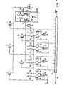
- the analog-to-digital converter circuit of Fig. 1 has sixteen comparison circuits denoted by the reference numerals 1 through 16, the upper inputs of which are connected to an input 17 of the circuit to which a signal to be converted can be applied.
- each comparison circuit is connected to a tap of a potential divider 19 connected to a reference voltage V ref , which tap corresponds in sequence to the numbering of the comparison circuits.
- V ref reference voltage
- the first tap of consecutive groups of taps is connected to the lower input of the comparison circuits 1, 5, 9, 13 which constitute a first group.
- the second tap of the consecutive groups of taps is connected to the lower input of the comparison circuits 2, 6, 10, which constitute a second group.
- the third tap of the groups of taps is connected to the lower input of the consecutive comparison circuits 3, 7, 11, 15 which constitute a third group and the fourth tap of the consecutive groups of taps is connected to the lower tap of the consecutive groups of taps is connected to the lower input of the comparison circuits 4, 8, 12, 16 which constitute a fourth group.
- Each comparison circuit has an upper and a lower output which are operative in opposite senses, that is to say, when its upper input receives a higher potential than its lower input, its upper output will be high relative to its lower output, and conversely when its upper input receives a lower potential than its lower input, its lower output becomes high relative to its upper output. This applies if the outputs of the comparison circuit were not connected together in the manner to be described hereinafter.
- comparison circuits 1, 5, 9, 13; 2, 6, 10, 14; 3, 7, 11 15 and 4, 8, 12, 16 the upper outputs ofthe comparison circuits 1, 5, 9 and 2, 6, 10; 3, 7, 11 and 4, 8, 12, respectively are connected to the lower outputs, operating in opposite senses of the subsequent comparison circuits 5, 9, 13 and 6, 10, 14; 7, 11, 15 and 8, 12, 16, respectively.
- the even outputs are connected to the base of a respective one of two transistors 61, 63; 65, 67; 69, 71 and 73, 75, respectively, whose emitters are interconnected and are connected to second inputs 77, 79, 81 and 83 of the differential amplifiers 45, 47, 4 9 and 51, respectively, and to current sources 85, 87, 89 and 91, respectively.
- Outputs 93, 95, 97 and 99 of the differential amplifiers 45, 47, 49 and 51, respectively, are connected to a code converter 101 which converts the signals obtained from these outputs and from two outputs 103 and 105 of two coarse comparison circuits 107 and 109 into a four-bit code which is supplied from an output combination 111 of the code converter 101.
- the coarse comparison circuits 107 and 109 detect levels being exceeded of the signal to be converted and applied to the lower inputs thereof, relative to the levels at the second tap in the second and fourth groups of taps, respectively, of the potential divider 19.
- the code converter 101 may comprise further circuits as described in United States Patent 4,456,904 (PHN 9925) in order to obtain faultless digital bit information from combinations of output signals from coarse and fine comparison circuits.
- the output signals at the outputs 93, 95, 97 and 99 of the differential amplifiers 45, 47, 49 and 51, respectively, upon the levels at the consecutive branches of the potential divider 19 being successively exceeded by this voltage will have a value as indicated in the following Table, and as will be further described hereinafter.
- Each comparison circuit comprises transistor pairs 113 115; 117, 119; 121, 125 and 127, 129, respectively.
- the emitters of these pairs are connected to current sources 131, 133, 135 and 137, respectively.
- the collectors of the transistors 113, 115, 117, 119, 121, 125, 127 and 129 are connected via resistors 139, 141, 143, 145, 147, 151 and 153, respectively, to a positive voltage. All these resistors have the same value, except for the resistors 139 and 153 whose value is half that of the others.
- the bases of the transistors 113, 117, 121 and 127 are connected to the signal input 17, and those of the transistors 115, 119, 125 and 129 are connected to the first, fifth, ninth and thirdteenth taps, respectively, on the potential divider 19.
- the collectors of the transistors 115 and 117 are connected together, likewise are those of the transistors 119 and 121 and those of the transistors 125 and 127.
- the bases of the transistors 21, 23, 24, 61 and 63 are connected to the collectors of the transistors 139, 121, 129, 117 and 127, respectively.
- the differential amplifier 45 has a transistor pair 155, 157 whose emitters are connected to a current source 159, whose collectors are connected via resistors 161, 163 to a positive voltage and whose bases are connected to the inputs 77 and 37 of the differential amplifier 45 the output 93 of which is connected to the collector of the transistor 157.
- the collector resistors 139, 141, 143, 145, 147, 149, 151, 153 of the transistors 113, 115, 117, 119, 121, 125, 127, 129 have a high value such that the voltage at the relevant collectors, is low when the current from one of the current sources 131, 133, 135, 137 passes through them.
- this current passes through the parallel circuit of the resistors 141 and 143, 145 and 147 or 149 and 151, the voltage at the relevant collectors is at a level between the low level and the supply voltage.
- the emitters of the group of transistors 21, 23, 24 assume the highest level of the collectors connected to the bases. This also applies to the group of transistors 61, 63.
- the voltage distribution at different points in the circuit will now be examined with reference to the following Table.
- the character H is used in this case for a supply voltage level and the character L is used for a low level.
- collector resistors 141 and 143, 145 and 147, 149 and 151 are shown as separate resistors, Generally, these will of course be replaced by a single resistor of half the value.
- comparison circuits When a large number of comparison circuits is used for the coarse bits, they may of course be grouped in a corresponding manner and be connected as described above for the comparison circuits for the fine bits.
Landscapes
- Engineering & Computer Science (AREA)
- Theoretical Computer Science (AREA)
- Analogue/Digital Conversion (AREA)
Applications Claiming Priority (2)
| Application Number | Priority Date | Filing Date | Title |
|---|---|---|---|
| NL8502510A NL8502510A (nl) | 1985-09-13 | 1985-09-13 | Analoog-digitaalomzetschakeling. |
| NL8502510 | 1985-09-13 |
Publications (2)
| Publication Number | Publication Date |
|---|---|
| EP0214703A1 true EP0214703A1 (de) | 1987-03-18 |
| EP0214703B1 EP0214703B1 (de) | 1990-06-13 |
Family
ID=19846552
Family Applications (1)
| Application Number | Title | Priority Date | Filing Date |
|---|---|---|---|
| EP86201562A Expired - Lifetime EP0214703B1 (de) | 1985-09-13 | 1986-09-10 | Analog-Digitalwandler |
Country Status (5)
| Country | Link |
|---|---|
| US (1) | US4686508A (de) |
| EP (1) | EP0214703B1 (de) |
| JP (1) | JPH0787370B2 (de) |
| DE (1) | DE3672051D1 (de) |
| NL (1) | NL8502510A (de) |
Families Citing this family (6)
| Publication number | Priority date | Publication date | Assignee | Title |
|---|---|---|---|---|
| US4922251A (en) * | 1988-11-30 | 1990-05-01 | American Telephone And Telegraph Company | Analog to digital interface circuit |
| US5117742A (en) * | 1989-04-28 | 1992-06-02 | Iwata Air Compressor Mfg. Co. Ltd. | Piston of composite material with c-shaped ring groove |
| JPH03140016A (ja) * | 1989-10-26 | 1991-06-14 | Sharp Corp | A/d変換器 |
| JPH03140017A (ja) * | 1989-10-26 | 1991-06-14 | Sharp Corp | 並列型a/d変換器 |
| JP3216830B2 (ja) * | 1992-06-30 | 2001-10-09 | ソニー株式会社 | アナログ信号比較回路 |
| US7286072B2 (en) * | 2005-02-15 | 2007-10-23 | Sanyo Electric Co., Ltd. | Analog-to digital converter and analog-to digital conversion apparatus |
Citations (1)
| Publication number | Priority date | Publication date | Assignee | Title |
|---|---|---|---|---|
| EP0070175A2 (de) * | 1981-07-10 | 1983-01-19 | Sony Corporation | Analog-Digital Umwandler |
Family Cites Families (1)
| Publication number | Priority date | Publication date | Assignee | Title |
|---|---|---|---|---|
| JPH0744454B2 (ja) * | 1983-09-12 | 1995-05-15 | ソニー株式会社 | A/dコンバータ |
-
1985
- 1985-09-13 NL NL8502510A patent/NL8502510A/nl not_active Application Discontinuation
-
1986
- 1986-09-02 US US06/903,046 patent/US4686508A/en not_active Expired - Fee Related
- 1986-09-10 DE DE8686201562T patent/DE3672051D1/de not_active Expired - Lifetime
- 1986-09-10 EP EP86201562A patent/EP0214703B1/de not_active Expired - Lifetime
- 1986-09-12 JP JP61214188A patent/JPH0787370B2/ja not_active Expired - Lifetime
Patent Citations (1)
| Publication number | Priority date | Publication date | Assignee | Title |
|---|---|---|---|---|
| EP0070175A2 (de) * | 1981-07-10 | 1983-01-19 | Sony Corporation | Analog-Digital Umwandler |
Non-Patent Citations (1)
| Title |
|---|
| IEEE INTERNATIONAL SOLID-STATE CIRCUITS CONFERENCE, San Francisco, US, 22nd-24th February 1984, vol. 27, conf. 31, pages 294,295,357, IEEE, New York, US; J.J. CORCORAN et al.: "A 400MHz 6b ADC" * |
Also Published As
| Publication number | Publication date |
|---|---|
| DE3672051D1 (de) | 1990-07-19 |
| NL8502510A (nl) | 1987-04-01 |
| JPS6265521A (ja) | 1987-03-24 |
| EP0214703B1 (de) | 1990-06-13 |
| JPH0787370B2 (ja) | 1995-09-20 |
| US4686508A (en) | 1987-08-11 |
Similar Documents
| Publication | Publication Date | Title |
|---|---|---|
| US5283579A (en) | Digital to analog converter having high multiplying bandwidth | |
| US4831379A (en) | Complementary voltage interpolation circuit | |
| US4338592A (en) | High accuracy digital-to-analog converter and transient elimination system thereof | |
| US4635036A (en) | Analog-to-digital converter | |
| KR940017236A (ko) | 아날로그 디지탈 컨버터 | |
| US4897656A (en) | Complementary voltage interpolation circuit with transmission delay compensation | |
| US4752766A (en) | Analog to digital converter | |
| EP0112180A2 (de) | Nach dem Parallelverfahren arbeitender Analog-Digitalwandler | |
| US4559522A (en) | Latched comparator circuit | |
| JPS6245729B2 (de) | ||
| EP0214703B1 (de) | Analog-Digitalwandler | |
| US3474440A (en) | Digital-to-analog converter | |
| US3573798A (en) | Analog-to-digital converter | |
| US4325054A (en) | Folding circuit for an analog-to-digital converter | |
| US4306224A (en) | Analog-to-digital converting apparatus | |
| GB2029143A (en) | Digital to analogue converter | |
| EP0782790B1 (de) | Analog-digitalwandler zur erzeugung von einem digitalen n-bit gray-code | |
| EP0082736B1 (de) | Analog-Digital-Wandler | |
| US4473818A (en) | Bipolar digital to analog converter | |
| EP0090667B1 (de) | Stromsummierender-Digitalanalogwandler | |
| US4306225A (en) | Digital-to-analog converting apparatus | |
| US4737766A (en) | Code converter with complementary output voltages | |
| US5034630A (en) | Logic circuit for use in D/A converter having ECL-type gate structure | |
| EP0121234B1 (de) | Decodierer für einen D/A Umsetzer | |
| JP2696905B2 (ja) | 並列型adコンバータの入力回路 |
Legal Events
| Date | Code | Title | Description |
|---|---|---|---|
| PUAI | Public reference made under article 153(3) epc to a published international application that has entered the european phase |
Free format text: ORIGINAL CODE: 0009012 |
|
| AK | Designated contracting states |
Kind code of ref document: A1 Designated state(s): DE FR GB IT |
|
| 17P | Request for examination filed |
Effective date: 19870702 |
|
| 17Q | First examination report despatched |
Effective date: 19890201 |
|
| GRAA | (expected) grant |
Free format text: ORIGINAL CODE: 0009210 |
|
| AK | Designated contracting states |
Kind code of ref document: B1 Designated state(s): DE FR GB IT |
|
| REF | Corresponds to: |
Ref document number: 3672051 Country of ref document: DE Date of ref document: 19900719 |
|
| ITF | It: translation for a ep patent filed | ||
| ET | Fr: translation filed | ||
| PLBE | No opposition filed within time limit |
Free format text: ORIGINAL CODE: 0009261 |
|
| STAA | Information on the status of an ep patent application or granted ep patent |
Free format text: STATUS: NO OPPOSITION FILED WITHIN TIME LIMIT |
|
| 26N | No opposition filed | ||
| ITTA | It: last paid annual fee | ||
| ITPR | It: changes in ownership of a european patent |
Owner name: CAMBIO RAGIONE SOCIALE;PHILIPS ELECTRONICS N.V. |
|
| REG | Reference to a national code |
Ref country code: FR Ref legal event code: CD |
|
| PGFP | Annual fee paid to national office [announced via postgrant information from national office to epo] |
Ref country code: FR Payment date: 19960925 Year of fee payment: 11 |
|
| PGFP | Annual fee paid to national office [announced via postgrant information from national office to epo] |
Ref country code: DE Payment date: 19961125 Year of fee payment: 11 |
|
| PGFP | Annual fee paid to national office [announced via postgrant information from national office to epo] |
Ref country code: GB Payment date: 19970829 Year of fee payment: 12 |
|
| PG25 | Lapsed in a contracting state [announced via postgrant information from national office to epo] |
Ref country code: FR Free format text: THE PATENT HAS BEEN ANNULLED BY A DECISION OF A NATIONAL AUTHORITY Effective date: 19970930 |
|
| PG25 | Lapsed in a contracting state [announced via postgrant information from national office to epo] |
Ref country code: DE Free format text: LAPSE BECAUSE OF NON-PAYMENT OF DUE FEES Effective date: 19980603 |
|
| REG | Reference to a national code |
Ref country code: FR Ref legal event code: ST |
|
| PG25 | Lapsed in a contracting state [announced via postgrant information from national office to epo] |
Ref country code: GB Free format text: LAPSE BECAUSE OF NON-PAYMENT OF DUE FEES Effective date: 19980910 |
|
| GBPC | Gb: european patent ceased through non-payment of renewal fee |
Effective date: 19980910 |
|
| PG25 | Lapsed in a contracting state [announced via postgrant information from national office to epo] |
Ref country code: IT Free format text: LAPSE BECAUSE OF NON-PAYMENT OF DUE FEES;WARNING: LAPSES OF ITALIAN PATENTS WITH EFFECTIVE DATE BEFORE 2007 MAY HAVE OCCURRED AT ANY TIME BEFORE 2007. THE CORRECT EFFECTIVE DATE MAY BE DIFFERENT FROM THE ONE RECORDED. Effective date: 20050910 |