EP0214870B1 - Système de commande d'instruction de transfert de données pour une mémoire d'extension - Google Patents
Système de commande d'instruction de transfert de données pour une mémoire d'extension Download PDFInfo
- Publication number
- EP0214870B1 EP0214870B1 EP19860307013 EP86307013A EP0214870B1 EP 0214870 B1 EP0214870 B1 EP 0214870B1 EP 19860307013 EP19860307013 EP 19860307013 EP 86307013 A EP86307013 A EP 86307013A EP 0214870 B1 EP0214870 B1 EP 0214870B1
- Authority
- EP
- European Patent Office
- Prior art keywords
- storage unit
- address
- memory
- extension
- data
- Prior art date
- Legal status (The legal status is an assumption and is not a legal conclusion. Google has not performed a legal analysis and makes no representation as to the accuracy of the status listed.)
- Expired - Lifetime
Links
Images




Classifications
-
- G—PHYSICS
- G06—COMPUTING OR CALCULATING; COUNTING
- G06F—ELECTRIC DIGITAL DATA PROCESSING
- G06F12/00—Accessing, addressing or allocating within memory systems or architectures
- G06F12/02—Addressing or allocation; Relocation
- G06F12/0207—Addressing or allocation; Relocation with multidimensional access, e.g. row/column, matrix
-
- G—PHYSICS
- G06—COMPUTING OR CALCULATING; COUNTING
- G06F—ELECTRIC DIGITAL DATA PROCESSING
- G06F12/00—Accessing, addressing or allocating within memory systems or architectures
- G06F12/02—Addressing or allocation; Relocation
- G06F12/08—Addressing or allocation; Relocation in hierarchically structured memory systems, e.g. virtual memory systems
- G06F12/10—Address translation
Definitions
- This invention relates to a system for controlling a data transfer instruction in a computer apparatus used in, for example, a super-high-speed computer apparatus for large-scale scientific and technological calculations, and a general purpose computer apparatus using an extension storage unit.
- the memory device is constituted by economical memories consisting of semiconductor memory elements having an operating speed far higher than that of a magnetic disk memory, although lower than that of a memory element constituting the main memory, and such a constituted memory device is used as an extension memory for relieving a shortage of capacity of the main memory.
- a vector processing unit In a prior art super-high-speed computer apparatus, access to the main memory is carried out by a vector processing unit, a channel processor, or the like, through a memory control unit.
- the vector processing unit consists of, for example, a vector unit and a scalar unit. Access to the main memory can be carried out independently from both the vector unit and the scalar unit.
- the extension memory is connected through the memory control unit to the main memory, and data can be transferred between the extension memory and the main memory.
- This data transfer is carried out with a page unit of, for example, 4KBytes, under the control of an operating system executed by the scalar unit, in such a manner that the extension memory services, in the same way, a so-called ultra-high-speed direct-access storage unit for paging.
- the extension memory is used as a high-speed memory unit, replacing the direct-access storage unit for storing a large amount of input/output data used in a huge application program.
- the system of Figure 1 includes a main memory 1, a memory control unit 2, a central processor unit 3, an extension memory 5 having an extension memory control, a channel processor 6, and a direct access storage 7.
- the access to the main memory 1 is carried out by the central processor unit 3 and the channel processor 6, through the memory control unit 2.
- the central processor unit 3 consists of, for example, a vector unit and a scalar unit.
- the access to the main memory 1 can be carried out independently from both the vector unit and the scalar unit.
- the extension memory 5 is connected through the memory control unit 2 with the main memory 1, and the data can be transferred between the extension memory 5 and the main memory 1.
- This data transfer is carried out with a page unit of, for example, 4KBytes, under the control of an operating system executed by the scalar unit, in such a manner that the extension memory 5 serves in the same way as a so-called ultra-high-speed direct access storage unit for paging.
- the extension memory 5 is used as a high-speed memory device, replacing the direct access storage unit, for storing a large amount of input/output data, used in a huge application program.
- FIG. 2 A system for controlling a data transfer instruction in a computer apparatus according to an embodiment of the present invention is shown in Fig. 2.
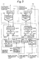
- the structure of the address control portion in the system of Fig. 2 is shown in Fig. 3.
- the system of Fig. 2 includes a main memory 1, a memory control unit 2, a central processor unit 3, a transfer control unit 4, and an extension memory 5.
- the central processor unit 3 may include a vector unit 31 and a scalar unit 32.
- the transfer control unit 4 includes an address conversion portion 41 for the extension memory, an address control portion 42, an address conversion portion 44 for the main memory, and a transfer control portion 45 having data buffers shift registers or registerfiles 451 and 452, and a buffer control portion 453.
- the extension memory 5 includes a data transfer control and an extension memory bank control portion 51.
- the transfer of data between the main memory 1 and the extension memory 5 is controlled by the transfer control unit 4 by the execution of instructions related to data transfer in the central processor unit 3.
- the address conversion portion 41 controls address conversion and the like from a logical address to a real address of the extension memory 5.
- the address conversion portion 44 controls address conversions concerning the main memory 1.
- the information for address conversion from a logical address to a real address of the extension memory 5 and the main memory 1 are set in the address conversion portion 41 and the address conversion portion 44, respectively, by the central processor unit 3.
- the detected data transfer instruction is transferred to the transfer control unit 4.
- the central processor unit 3 By the operation of the central processor unit 3, the designation of the beginning addresses of memory regions of the extension memory 5 and the main memory 1 given as operand of the instruction, a increased value of an address for the calculation of each of the elements of the vector data, the number of such elements, and the like, are set in an address register in the address control portion 42. Also, the transmission of control information concerning a transfer mode and the direction of data transfer determined by the operation code of the data transfer instruction, and the like, is carried out.
- the address control portion 42 By the operation of the address control portion 42, the desired logical addresses for each of access units are generated successively in accordance with the designated address information and transfer mode, the logical address of the extension memory 5 is supplied to the address conversion portion 41, and the logical address of the main memory 1 is supplied to the address conversion portion 44.
- the address conversion portion 41 and the address conversion portion 44 By the operation of the address conversion portion 41 and the address conversion portion 44, the conversion from a logical address to a real address in accordance with the address conversion information set in the address conversion portion 41 and the address conversion portion 44 is carried out, the transmission of real addresses to the extension memory 5 and the main memory 1 is carried out, the request for access operation by this transmission of real addresses is carried out, and accordingly, an access to the desired vector data element is carried out.
- the data read from the extension memory 5 is registered in the data buffer 451, and the data registered in the data buffer is then written into the main memory 1, while the data read from the main memory 1 is written into the extension memory 5 through the data buffer452.
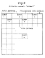
- FIGs. 4, 5A, 5B and 6 show the kinds of operations concerning data transfer.
- Figure 4 shows the "Distance” operation
- Figs. 5A and 5B show the "Indirect” operation and the "List Vector”
- Fig. 6 shows the "Block” operation.
- the instruction consists of an operation code portion and an operand designation portion.
- the operation code portion indicates an operation code OP concerning the main memory to the extension memory or the extension memory to the main memory transfer.
- the operand designation portion includes R1 for selection of the register, X1 and B1 for the logical address of the main memory, and X2, B2, and D2 for the logical address of the extension memory.
- OP There are a number of kinds of OP.
- a distance load instruction For example, a distance store instruction, a indirect designation load instruction, a indirect designation store instruction, a block load instruction, and a block store instruction.
- load represents the data transfer from the main memory to the extension memory
- store represents the data transfer from the extension memory to the main memory
- the pitch distances (intervals) of data elements in the extension memory 5 is designated by the list vector preliminarily provided in the main memory 1.
- the address of the memory of the list vector is designated by the content of the register designated by R1 of the instruction.
- the number of the data elements to be transferred is designated in the same manner as in the above-described case.
- the number of data elements to be transferred is designated by R1.
- R1 the number 512, which is the region of 4 K Bytes at 8 Bytes per element, is designated by "0”
- the number 8192 which is the region of 64 K Bytes at 8 Bytes per element, is designated by "1".
- the operation of the system of Fig. 2 is as follows.
- the fetched instruction is transferred to the transfer control unit 4.
- the effective logical addresses of the first and second operands are calculated by the transfer control unit 4 under a known control, and the calculated addresses are set in a predetermined register in the address control portion 42 in the transfer control unit 4.
- the contents of the register designated by R1 and the register next to the register designated by R1 are set in a predetermined register in the address control portion 42.
- the designated number of the elements determined by the value of R1 is set in a predetermined register in the address control portion 42.
- the logical address of the first operand (X1, B1) is set in the register 4211
- the logical address of the second operand (X2, B2, D2) is set in the register 4213
- the content of the register designated by R1 is set in the register 4212
- the content of the register next to the register designated by R1 is set in the register 4215.
- the number of sequence of elements determined by R1 is set in the register 4215.
- the kind of operation concerning transfers from the main memory to extension memory or the extension memory to main memory is designated by setting the instruction code (OP code) in the register 4214.
- the kind of operation is discriminated by the register 4214. Where it is discriminated as an indirect designation store, the access to the main memory 1 in accordance with the content of the register 4212 is carried out, and the designated list vector is read from the main memory 1 to the list vector register 4216.
- the list vector is a vector having a variable length representing pitch distances (intervals) of data elements.
- the content of the register 4213 is set through the adder 4231 into the register 4241, and the content of the register 4241 is then transmitted to the address conversion portion 41.
- the data of the register 4241 is converted through the address conversion table which is preliminarily set in the address conversion table 412 into the data of the real address, and the obtained converted real address is set in the register 411.
- the lower bits of the data of the register 4241 may be added to the real address set in the register 411 as lower bits.
- a real address for the extension memory 5 is obtained in the register 411.
- the address registered in the register 411 is transmitted to the extension memory control portion 51, and an access to the extension memory 5 is carried out.
- the data are sequentially written into the extension memory 5 with the beginning data of, for example, 8 Bytes.
- the "store” operation the data of 8 Bytes read from the extension memory 5 is registered temporarily in the end bits of the data buffer 451, and the registered data is then written into the main memory 1.
- the content of the register 4241 is returned to the input of the adder 4231.
- the returned content is added to the content of the register 4212 or the content of one item selected sequentially from the list vector registers 4216 in accordance with a transfer mode determined by the operation code.
- the result of this addition is set again in the register 4241.
- the control similar to the above-described control is carried out using the set result of the addition as the logical address for the next element.
- the content of the register 4211 is set through the adder 4232 into the register 4242.
- the address in the register 4242 is converted through the address conversion table 442 in the address conversion table 442 into the data in the register 441.
- a real address for the main memory 1 is obtained in the register 441.
- the address registered in the register 441 is transmitted to the memory control unit 2, and an access to the main memory 1 is carried out.
- the data of the beginning 8 Bytes of the data buffer 451 is written into the main memory 1.
- the data of 8 Bytes read from the main memory 1 is temporarily registered into the data buffer 452, and this registered data is then written into the extension memory 5.
- the content of the register 4242 is returned to the input of the adder 4232, and the returned content is added to the value representing the pitch distance which is set in the register 4217.
- the result of the addition is again set in the register 4242.
- the control similar to the above-described control is carried out using the set result as the logical address for the next element.
- the synchronization of the accesses to the extension memory 5 and to the main memory 1 is monitored and controlled by the transfer control portion 45. Under these monitoring and control processes, the address generation, the address conversion, and the access to the extension memory or to the main memory is carried out by the address control portion 42, the address conversion portion 41, and the address conversion portion 44.
- the execution of the data transfer instruction is completed after a predetermined number, set in the register 4215, of the above-described control is carried out.
- FIG. 8 Another example of the instruction for data transfer and the descriptor is shown in Figs. 8 and 9.
- a data transfer instruction is shown.
- the instruction consists of an operation code and the addresses X, B, and D which designate the beginning addresses of the access descriptor which is preliminarily set in the main memory 1.
- a descriptor related to the instruction of Fig. 8 is shown.
- the descriptor consists of OP, N(NUMBER OF ELEMENTS), ADR1, ADR2, PITCH DISTANCE, ADR3, and so on.
- OP is an operation code which represents the transferring direction, i.e., load or store, and the transfer mode.
- N(NUMBER OF ELEMENTS) represents the number of elements to be transferred.
- ADR1 represents the logical address of the beginning of the memory region of the main memory 1.
- ADR2 represents the logical address of the beginning of the memory region of the extension memory 5.
- ADR3 represents the address of the memory region of the list vector in the cases of the indirect designation load and the INDIRECT designation store.
- PITCH DISTANCE represents the constant interval of elements in the cases of distance load and distance store.
- an advantage is attained in that it is possible to add the functions concerning data transfer without changes of the transfer control unit 4 and the data transfer instruction shown in Fig. 8, by changing the content of the access descriptor, and, if necessary, by changing the constitution of the transfer control device 4 accordingly.
Landscapes
- Engineering & Computer Science (AREA)
- Theoretical Computer Science (AREA)
- Physics & Mathematics (AREA)
- General Engineering & Computer Science (AREA)
- General Physics & Mathematics (AREA)
- Mathematical Physics (AREA)
- Complex Calculations (AREA)
- Executing Machine-Instructions (AREA)
- Memory System Of A Hierarchy Structure (AREA)
- Memory System (AREA)
Claims (1)
- Un système destiné à commander une instruction de transfert de données dans un ordinateur comportant un processeur (3), une unité de mémoire centrale (1) qui est destinée à enregistrer des données à traiter par le processeur, et une unité de mémoire d'extension (5) qui est destinée à échanger des données avec l'unité de mémoire centrale, caractérisé par des moyens (42, 4213, 4211, 4214) qui sont destinés à conserver une première adresse logique de désignation de début, qui est destinée à désigner le début d'une région de mémoire de l'unité de mémoire d'extension, une seconde adresse logique de désignation de début qui est destinée à désigner le début d'une région de mémoire de l'unité de mémoire centrale, et une désignation d'un mode de transfert, qui sont toutes désignées par une instruction de transfert de données que doit exécuter le processeur; des moyens (4231, 4232) qui sont destinés à faire la somme de distances correspondant à des positions de mémoire dans l'unité de mémoire d'extension et dans l'unité de mémoire centrale, conformément à la désignation du mode de transfert, et à générer de façon correspondante une troisième adresse logique qui doit faire l'objet d'une opération d'accès dans l'unité de mémoire d'extension, à partir de la première adresse logique de l'unité de mémoire d'extension, et une quatrième adresse logique qui doit faire l'objet d'une opération d'accès dans l'unité de mémoire centrale, à partir de la seconde adresse logique de l'unité de mémoire centrale; des moyens (41) qui sont destinés à convertir la troisième adresse logique devant faire l'objet d'une opération d'accès, pour fournir l'adresse réelle de désignation de début pour l'unité de mémoire d'extension; et des moyens (44) qui sont destinés à convertir la quatrième adresse logique pour fournir l'adresse réelle de désignation de début pour l'unité de mémoire centrale; dans lequel un transfert de données est accompli entre une région de mémoire de l'unité de mémoire d'extension qui est désignée par l'adresse réelle de désignation de début pour l'unité de mémoire d'extension, et une région de mémoire de l'unité de mémoire centrale qui est désignée par l'adresse réelle de désignation de début pour l'unité de mémoire centrale.
Applications Claiming Priority (2)
| Application Number | Priority Date | Filing Date | Title |
|---|---|---|---|
| JP60202011A JPS6261132A (ja) | 1985-09-12 | 1985-09-12 | デ−タ転送命令制御方式 |
| JP202011/85 | 1985-09-12 |
Publications (3)
| Publication Number | Publication Date |
|---|---|
| EP0214870A2 EP0214870A2 (fr) | 1987-03-18 |
| EP0214870A3 EP0214870A3 (en) | 1989-01-11 |
| EP0214870B1 true EP0214870B1 (fr) | 1993-02-10 |
Family
ID=16450443
Family Applications (1)
| Application Number | Title | Priority Date | Filing Date |
|---|---|---|---|
| EP19860307013 Expired - Lifetime EP0214870B1 (fr) | 1985-09-12 | 1986-09-11 | Système de commande d'instruction de transfert de données pour une mémoire d'extension |
Country Status (5)
| Country | Link |
|---|---|
| EP (1) | EP0214870B1 (fr) |
| JP (1) | JPS6261132A (fr) |
| CA (1) | CA1261480A (fr) |
| DE (1) | DE3687726T2 (fr) |
| ES (1) | ES2001675A6 (fr) |
Families Citing this family (8)
| Publication number | Priority date | Publication date | Assignee | Title |
|---|---|---|---|---|
| US5127094A (en) * | 1987-11-09 | 1992-06-30 | Hitachi, Ltd. | Virtual storage type computer system |
| JP2965987B2 (ja) * | 1988-02-22 | 1999-10-18 | 株式会社日立製作所 | データ処理システム |
| JP3005626B2 (ja) * | 1988-09-21 | 2000-01-31 | 株式会社日立製作所 | データ処理システムおよびデータ転送方法 |
| US5159677A (en) * | 1988-11-21 | 1992-10-27 | International Business Machines Corp. | Method and system for storing data in and retrieving data from a non-main storage virtual data space |
| JP2513024B2 (ja) * | 1989-03-16 | 1996-07-03 | 日本電気株式会社 | 拡張記憶アドレス制御方式 |
| JPH036754A (ja) * | 1989-06-05 | 1991-01-14 | Fujitsu Ltd | データ転送制御方式 |
| US5237668A (en) * | 1989-10-20 | 1993-08-17 | International Business Machines Corporation | Process using virtual addressing in a non-privileged instruction to control the copying of a page of data in or between multiple media |
| JP3219826B2 (ja) * | 1992-02-21 | 2001-10-15 | 日本電気株式会社 | 情報処理装置 |
Family Cites Families (6)
| Publication number | Priority date | Publication date | Assignee | Title |
|---|---|---|---|---|
| FR1508747A (fr) * | 1966-01-20 | 1968-03-14 | ||
| US3609665A (en) * | 1970-03-19 | 1971-09-28 | Burroughs Corp | Apparatus for exchanging information between a high-speed memory and a low-speed memory |
| GB1531261A (en) * | 1975-09-27 | 1978-11-08 | Nat Res Dev | Computer store mechanisms |
| FR2438296B1 (fr) * | 1978-10-05 | 1986-06-13 | Burroughs Corp | Reseau d'alignement avec acces parallele |
| JPS59167761A (ja) * | 1983-03-14 | 1984-09-21 | Hitachi Ltd | 計算機システム |
| JPS60142450A (ja) * | 1983-12-28 | 1985-07-27 | Fujitsu Ltd | 記憶システム |
-
1985
- 1985-09-12 JP JP60202011A patent/JPS6261132A/ja active Pending
-
1986
- 1986-09-05 CA CA000517633A patent/CA1261480A/fr not_active Expired
- 1986-09-10 ES ES8601754A patent/ES2001675A6/es not_active Expired
- 1986-09-11 DE DE19863687726 patent/DE3687726T2/de not_active Expired - Fee Related
- 1986-09-11 EP EP19860307013 patent/EP0214870B1/fr not_active Expired - Lifetime
Also Published As
| Publication number | Publication date |
|---|---|
| EP0214870A3 (en) | 1989-01-11 |
| DE3687726D1 (de) | 1993-03-25 |
| JPS6261132A (ja) | 1987-03-17 |
| EP0214870A2 (fr) | 1987-03-18 |
| CA1261480A (fr) | 1989-09-26 |
| DE3687726T2 (de) | 1993-05-27 |
| ES2001675A6 (es) | 1988-06-01 |
Similar Documents
| Publication | Publication Date | Title |
|---|---|---|
| EP0240032B1 (fr) | Processeur à vecteur avec possibilité de compression/expansion de données vecteur | |
| EP0054888B1 (fr) | Système de traitement de données à commande de mémoire principale et de mémoire tampon | |
| Watson | The TI ASC: a highly modular and flexible super computer architecture | |
| US4524416A (en) | Stack mechanism with the ability to dynamically alter the size of a stack in a data processing system | |
| US4382278A (en) | Hierarchial memory system with microcommand memory and pointer register mapping virtual CPU registers in workspace cache #4 and main memory cache | |
| US3647348A (en) | Hardware-oriented paging control system | |
| JPH0512750B2 (fr) | ||
| US5297255A (en) | Parallel computer comprised of processor elements having a local memory and an enhanced data transfer mechanism | |
| US4639862A (en) | Computer system | |
| EP0214870A2 (fr) | Système de commande d'instruction de transfert de données pour une mémoire d'extension | |
| US3546680A (en) | Parallel storage control system | |
| US4096570A (en) | Subchannel memory access control system | |
| EP0220990B1 (fr) | Système de commande de mémoire tampon | |
| US4301514A (en) | Data processor for processing at one time data including X bytes and Y bits | |
| US5506980A (en) | Method and apparatus for parallel processing of a large data array utilizing a shared auxiliary memory | |
| US4816992A (en) | Method of operating a data processing system in response to an interrupt | |
| US5247695A (en) | Vector processor with byte access of memory | |
| US6195747B1 (en) | System and method for reducing data traffic between a processor and a system controller in a data processing system | |
| EP0326164B1 (fr) | Calculateur parallèle constitué d'éléments de calcul ayant une mémoire locale et un mécanisme de transfert de données amélioré | |
| US4561071A (en) | Storage system having buffer storage | |
| GB2039106A (en) | Number format conversion in computer Fig 3A | |
| US3918031A (en) | Dual mode bulk memory extension system for a data processing | |
| SU993262A1 (ru) | Устройство дл обработки информации | |
| WO1996012230A1 (fr) | Systeme et procede de traitement de donnees de memoire et systeme de telecommunications comprenant ce systeme de traitement | |
| JP2895892B2 (ja) | データ処理装置 |
Legal Events
| Date | Code | Title | Description |
|---|---|---|---|
| PUAI | Public reference made under article 153(3) epc to a published international application that has entered the european phase |
Free format text: ORIGINAL CODE: 0009012 |
|
| AK | Designated contracting states |
Kind code of ref document: A2 Designated state(s): DE FR GB |
|
| PUAL | Search report despatched |
Free format text: ORIGINAL CODE: 0009013 |
|
| AK | Designated contracting states |
Kind code of ref document: A3 Designated state(s): DE FR GB |
|
| 17P | Request for examination filed |
Effective date: 19890622 |
|
| 17Q | First examination report despatched |
Effective date: 19920128 |
|
| GRAA | (expected) grant |
Free format text: ORIGINAL CODE: 0009210 |
|
| AK | Designated contracting states |
Kind code of ref document: B1 Designated state(s): DE FR GB |
|
| REF | Corresponds to: |
Ref document number: 3687726 Country of ref document: DE Date of ref document: 19930325 |
|
| ET | Fr: translation filed | ||
| PLBE | No opposition filed within time limit |
Free format text: ORIGINAL CODE: 0009261 |
|
| STAA | Information on the status of an ep patent application or granted ep patent |
Free format text: STATUS: NO OPPOSITION FILED WITHIN TIME LIMIT |
|
| 26N | No opposition filed | ||
| PGFP | Annual fee paid to national office [announced via postgrant information from national office to epo] |
Ref country code: DE Payment date: 20000904 Year of fee payment: 15 |
|
| PGFP | Annual fee paid to national office [announced via postgrant information from national office to epo] |
Ref country code: GB Payment date: 20000906 Year of fee payment: 15 |
|
| PGFP | Annual fee paid to national office [announced via postgrant information from national office to epo] |
Ref country code: FR Payment date: 20000912 Year of fee payment: 15 |
|
| PG25 | Lapsed in a contracting state [announced via postgrant information from national office to epo] |
Ref country code: GB Free format text: LAPSE BECAUSE OF NON-PAYMENT OF DUE FEES Effective date: 20010911 |
|
| GBPC | Gb: european patent ceased through non-payment of renewal fee |
Effective date: 20010911 |
|
| PG25 | Lapsed in a contracting state [announced via postgrant information from national office to epo] |
Ref country code: DE Free format text: LAPSE BECAUSE OF NON-PAYMENT OF DUE FEES Effective date: 20020501 |
|
| PG25 | Lapsed in a contracting state [announced via postgrant information from national office to epo] |
Ref country code: FR Free format text: LAPSE BECAUSE OF NON-PAYMENT OF DUE FEES Effective date: 20020531 |
|
| REG | Reference to a national code |
Ref country code: FR Ref legal event code: ST |