EP0216163A2 - Optical measuring apparatus - Google Patents
Optical measuring apparatus Download PDFInfo
- Publication number
- EP0216163A2 EP0216163A2 EP86111673A EP86111673A EP0216163A2 EP 0216163 A2 EP0216163 A2 EP 0216163A2 EP 86111673 A EP86111673 A EP 86111673A EP 86111673 A EP86111673 A EP 86111673A EP 0216163 A2 EP0216163 A2 EP 0216163A2
- Authority
- EP
- European Patent Office
- Prior art keywords
- light
- wave length
- measuring apparatus
- photo
- optical
- Prior art date
- Legal status (The legal status is an assumption and is not a legal conclusion. Google has not performed a legal analysis and makes no representation as to the accuracy of the status listed.)
- Withdrawn
Links
Images


Classifications
-
- G—PHYSICS
- G01—MEASURING; TESTING
- G01D—MEASURING NOT SPECIALLY ADAPTED FOR A SPECIFIC VARIABLE; ARRANGEMENTS FOR MEASURING TWO OR MORE VARIABLES NOT COVERED IN A SINGLE OTHER SUBCLASS; TARIFF METERING APPARATUS; MEASURING OR TESTING NOT OTHERWISE PROVIDED FOR
- G01D5/00—Mechanical means for transferring the output of a sensing member; Means for converting the output of a sensing member to another variable where the form or nature of the sensing member does not constrain the means for converting; Transducers not specially adapted for a specific variable
- G01D5/26—Mechanical means for transferring the output of a sensing member; Means for converting the output of a sensing member to another variable where the form or nature of the sensing member does not constrain the means for converting; Transducers not specially adapted for a specific variable characterised by optical transfer means, i.e. using infrared, visible, or ultraviolet light
- G01D5/32—Mechanical means for transferring the output of a sensing member; Means for converting the output of a sensing member to another variable where the form or nature of the sensing member does not constrain the means for converting; Transducers not specially adapted for a specific variable characterised by optical transfer means, i.e. using infrared, visible, or ultraviolet light with attenuation or whole or partial obturation of beams of light
- G01D5/34—Mechanical means for transferring the output of a sensing member; Means for converting the output of a sensing member to another variable where the form or nature of the sensing member does not constrain the means for converting; Transducers not specially adapted for a specific variable characterised by optical transfer means, i.e. using infrared, visible, or ultraviolet light with attenuation or whole or partial obturation of beams of light the beams of light being detected by photocells
Definitions
- the present invention relates to an optical measuring apparatus for optically measuring physical quantities such as magnetic field, pressure and electric field.
- FIG. 1 is a block diagram showing, for example, a magnetic-field measuring apparatus for measuring the magnetic field of the conventional optical measuring apparatus
- reference numeral 1 designates a light source
- 2 designating a transmission path (hereinafter referred to as an optical fiber) formed of an optical fiber connected with the light source 1 at one end thereof for transmitting light from the light source 1
- 3 designating a self-focusing lens mounted on the other end of the optical fiber 2 for changing beams of light radiated from the optical fiber 2 to parallel beams of light
- 4 designating a polarizer for changing the parallel beams of light obtained by the self-focusing lens 3 to a linearly polarized light
- 5 designating a magnetic optical element arranged in a magnetic field to be measured for rotating a plane of polarization of the linearly polarized light from the polarizer 4 in correspondence to the magnetic field to be measured.
- 7 designating an analyzer for dividing the optical output from the magnetic optical element 5 into polarized ingredients meeting at right angles to each other; 8a, 8b designating lenses for collecting the lights having been divided by the analyzer 7 and making them incident upon optical fibers 9a, 9b; 10a, 10b designating photo-detectors mounted on one end of the optical fibers 9a, 9b for converting the lights transmitted by the optical fibers 9a, 9b into electric signals il, i2; 11 designating an adder for adding the electric signals il, 12 having been converted by the photo-detectors 10a, 10b; 12 designating a subtracter for subtracting the electric signal i2 from the electric signal il; and 13 designating a divider for dividing the output from the subtracter 12 by the output from the adder 11.
- a light radiated from the light source 1 is transmitted by the optical fiber 2, changed to parallel beams of light by the self-focusing lens 3, and converted into the linearly polarized light by the polarizer 4.
- This linearly polarized light is incident upon the magnetic optical element 5 to rotate the plane of polarization thereof in correspondence to the magnetic field to be measured.
- the light, whose plane of polarization is rotated, is divided into two polarized ingredients P p ,P s meeting at right angles to each other by the analyzer 7 arranged at an angle of 45° to the linearly polarized light of the output from the polarizer 4.
- the divided lights P p , P s are collected by the lenses 8a, 8b and incident upon the photo-detectors 10a, 10b through the optical fibers 9a, 9b to be photoelectrically converted, respectively.
- An optical strength of the divided lights P p , P s is expressed as follows, respectively: wherein OF is an angle of rotation of the plane of polarization by the magnetic optical element 5; and P o is a strength prior to the incidence upon the analyzer 7.
- the above described is an example of the conventional magnetic field measuring apparatus, in which the pressure and electric field can be measured by using a photoelastic " element and a Pockels element in place of the magnetic optical element 6 in the same construction.
- the conventional optical measuring apparatus have the above described construction, it is necessary to use a plurality of transmission paths (optical fibers 9a, 9b) between the analyzer 7 and the photo-detectors, whereby the problem has occurred in that a difference in optical loss and a fluctuation in optical loss between a plurality of transmission paths lead to errors of measurement and the like.
- shielding means made from a material permeable to light having a first wave length and shielding light having a second wave length, for changing a shielding ratio of the light having the second wave length in correspondence to a physical quantity to be measured is arranged in transmission paths through which these two kinds of lights having different wave lengths are transmitted, the lights having the first and second wave length being radiated from two light sources and transmitted through the transmission paths, the lights having two kinds of wave length, which passed through the shielding means, being received by the photo-detectors, and a ratio of the quantities of the received lights being operated to determine the physical quantity.
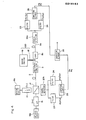
- FIG. 2 is a block diagram showing a first preferred embodiment of an optical measuring apparatus according to the present invention
- reference numeral s 14, 15 designate light source s for radiating light having a wave length of ⁇ 1 and light having a wave length of ⁇ 2 , respectively, said light sources 14, 15 being alternately switched on by means of a driving circuit 16.
- the light-source planes of the light sources 14, 15 face to a beam splitter 17, an end plane of a single optical fiber 2 for transmitting lights from the light sources 14, 15 facing to said beam splitter 17, and the optical fiber 2 being provided with a self-focusing lens 3 at an end thereof for changing the lights radiated from the light sources 14, 15 to parallel beams of light.
- an optical fiber 9a is connected with a lens 8a arranged opposite to the self-focusing lens 3.
- a semiconductor 18 having the property of being permeable to only the light having a wave length of ⁇ 1 is arranged in a space between the self-focusing lens 3 and the lens 8a,so as to usually shield the parallel beams of light passing through,said space, a sensor portion 19 for shifting the semiconductor 18 in reply to a physical quantity, being connected with the semiconductor 18.
- the semiconductor 18 is adapted to shift in the direction vertical to an optical path of the parallel beams of light by the action of the sensor portion 19 and is retreated from a part of the optical path of the parallel beams of light in correspondence to the shift.
- Shielding means 100 is composed of said semiconductor 18 and said sensor portion 19.
- the optical fiber 9a is connected with a photo-detector 20a which receives light having a wave length of ⁇ 1 , which passed through the semiconductor 18 or passed by the semiconductor 18 without being incident upon thd semiconductor 18, and light having a wave length of a 2 , which passed by the semiconductor 18 without being shielded with the shift of the semiconductor 18, to convert them into electric signals.
- a photo-detector 20b faces to the beam splitter 17 and receives lights radiated from the light sources 14, 15 to convert them into electric signals.
- the photo-detectors 20a, 20b are connected with an A/D converter 21 to convert output signals of the photo-detectors 20a, 20b into digital values.
- the A/D converter 21 is connected with a computing element 22 for operating a physical quantity on the basis of the converted outputs therefrom.
- a signal which synchronized with a driving signal for switching on the light sources 14, 15, is sent to the A/D converter 21 and the computing element 22, respectively, from the driving circuit 16, the A/D converter 21 digitalizing an input value in synchronization with the synchronizing signal from the driving circuit 16, and the computing element 22 similarly specifying an input signal in synchronization with the driving circuit 16.
- the lights having a wave length of ⁇ 1 and ⁇ 2 radiated from the light sources 14, 15, which are alternately switched on by means of the driving circuit 16, are incident upon the optical fiber 2 through the beam splitter 17 and a part of them is incident upon the photo-detector 20b.
- the light incident upon the optical fiber 2 is changed to parallel beams of light by the self-focusing lens 3 and the parallel beams of light are incident upon a gap portion where the semiconductor 18 is positioned.
- the semiconductor 18 has steep absorption edge wave-length characteristics such as a spectral wave form as shown in Fig.
- the semiconductor 18 is impermeable to a light having the wave length X2 as shown by a spectral wave form b being shorter than an absorption edge wave length,but almost completely permeable to a light having the wave length of ⁇ 1 as shown by a spectral wave form c being longer than the absorption edge wave length. Accordingly, of the quantity of light incident upon the lens 8a, the quantity of the light having the wave length of ⁇ 1 is constant regardless of the shift of the semiconductor 18 but the quantity of the light having the wave length of ⁇ 2 is dependent upon the shift of the semiconductor 18.
- the light which passes through the gap portion where the semiconductor 18 is positioned and is collected by the lens 8a, is incident upon the photo-detector 20a through the optical fiber 9a.
- the photo-detectors 20a, 20b convert the incident light into an electric quantity and put outputs therefrom in the A/D converter 21.
- the A/D converter 21 converts the input into a digital value in synchronization with the switching-on of the light sources 14, 15. In this time, also the outputs of the photo-detectors 20a, 20b in the case where both the light source 14 and the light source 15 are switched off are converted into digital values.
- the computing element 22 receives an output P 1 (the photo-detector 20a) and an output P 2 (the photo-detector 20b) in synchronization with the switching-on of the light source 14 (wave length of ⁇ 1 ), an output P 3 (the photo-detector 20a) and an output P 4 (the photo-detector 20b) in synchronization with the switching-on of the light source 15 (wave length of X2), and an output P A (the photo-detector 20a) and an output Pg(the photo-detector 20b) when switched off, to operate ((P 3 - P A )/(P 1 - P A ) ⁇ / ⁇ (P 4 - P B )/(P 2 - P B ) ⁇ , whereby measuring a quantity of shift of the semiconductor 18, in short the physical quantity, on the basis of a relation among the operated value, the previously set quantity of shift of the semiconductor 18 and the physical quantity.
- P 1 - P A , P 3 - P A , P 2 - P B and P 4 - P B show true outputs of the lights having a wave length of ⁇ 1 and ⁇ 2 from the photo-detectors 20a, 20b. An influence by a dark current of the photo-detectors is eliminated.
- (P 3 -P A )/(P 1 - P A ) in said operated value shows a ratio of a quantity of the light having a wave length of ⁇ 2 , which passed by the semiconductor 18, to a quantity of the light having a wave length of ⁇ 1 , which passed through or by the semiconductor 18, in short the quantity of shift of the semiconductor 18 (the physical quantity to be measured).
- (P 4 -P B )/(P 2 -P B ) shows a ratio of a quantity of light radiated from the light source 15 to a quantity of light radiated from the light source 14. Accordingly, since a quotient of a value of the ratio of a quantity of the light having a wave length of A 2 , which passed by the semiconductor 18, to a quantity of the light having a wave length of ⁇ 1 , which passed through or by the semiconductor 18, by a value of the ratio of a quantity of light radiated from the light source 15 to a quantity of light radiated from the light source 14 is determined, an exact quantity of shift of the semiconductor 18 can be obtained even though the light sources 14, 15 show any fluctuation.
- each of the light sources 14, 15 fluctuates in a range between a broken line and a dotted chain line shown in Fig. 3 in dependence upon a change in circumferential temperature of the semiconductor 18 and the light sources 14, 15, they are not influenced by temperature change if the spectral wave form a of the absorption edge wave length does not cross the spectral wave forms b, c of the lights having a wave length of ⁇ 1 , X2 radiated from the light sources 14, 15. Therefore, the light sources 14, 15, which radiate lights each having a wave length quite different from the spectral wave length of the absorption edge wave length of the semiconductor 18, are preferably used.
- an amorphous semiconductor can also be used as the semiconductor 18, a crystalline semiconductor is preferably used in view of the achievement of more excellent absorption edge wave-length characteristics.
- any material capable of shifting the semiconductor 18 in correspondence to a physical quantity (such as pressure, magnetic field and electric field) may be used as the sensor portion 19.
- luminous diodes shown by LED in the drawing for short
- driving circuits 16a, 16b in the form of modulated light having frequencies different from each other.
- photo-detectors 20a, 20b are connected with filters 23, 24 which transmit only electric signals corresponding to the different frequencies.
- 25, 26 designate computing elements for dividing an output from a pair of filters 23, 24 by an output from another pair of filters 23, 24, said computing elements 25, 26 being connected with a computing element 22 for dividing an output from the computing element 26 by an output from the computing element 25 to operate the physical quantity.
- the treatment can be carried out by analog signals, so that an A/D converter is not required.
- Other constructions are similar to those in the first preferred embodiment shown in Fig. 2.
- the light sources 14, 15 are pulsedly driven by frequencies different from each other, in other words, the driving circuits 16a, 16b, so as to be switched on in the form of modulated light and receive an output from the photo-detectors 20a, 20b through the filters 23, 24, respectively, the filter 23 putting out the outputs (P I , P 2 ) from the light source 14, and the filter 24 putting out the outputs (P 3 , P 4 ) from the light source 15.
- a division of an output from the filter 24 by an output from the filter 23 is carried out by the computing elements25, 26 for the photo-detectors20a, 20b, respectively, a division of an output from the computing element 26 by an output from the computing element 25 (the output from the computing element 25 is P 4 /P 2 and the output from the computing element 26 is P 3 /P 1 ) being carried out by a computing element 22 to obtain the quotient (P 3 /P 1 )/(P 4 /P 2 ), whereby the quantity of shift of the semiconductor 18, in short the physical quantity, is measured without being influenced by the loss of the optical transmission path or the fluctuation of the light source.
- the filter in the second preferred embodiment Since only the signal having the specified frequency passes through the filter in the second preferred embodiment, it is unnecessary to take the outputs P A , P B , which are dark-current ingredients, in the first preferred embodiment into consideration.
- the physical quantity can be measured in the form of analog signalsas it is.
Landscapes
- Physics & Mathematics (AREA)
- General Physics & Mathematics (AREA)
- Investigating Or Analysing Materials By Optical Means (AREA)
- Measuring Fluid Pressure (AREA)
Abstract
Description
- The present invention relates to an optical measuring apparatus for optically measuring physical quantities such as magnetic field, pressure and electric field.
- Referring now to Fig. 1 which is a block diagram showing, for example, a magnetic-field measuring apparatus for measuring the magnetic field of the conventional optical measuring apparatus, reference numeral 1 designates a light source, 2 designating a transmission path (hereinafter referred to as an optical fiber) formed of an optical fiber connected with the light source 1 at one end thereof for transmitting light from the
light source 1, 3 designating a self-focusing lens mounted on the other end of theoptical fiber 2 for changing beams of light radiated from theoptical fiber 2 to parallel beams of light, 4 designating a polarizer for changing the parallel beams of light obtained by the self-focusinglens 3 to a linearly polarized light, and 5 designating a magnetic optical element arranged in a magnetic field to be measured for rotating a plane of polarization of the linearly polarized light from thepolarizer 4 in correspondence to the magnetic field to be measured. In addition, 7 designating an analyzer for dividing the optical output from the magneticoptical element 5 into polarized ingredients meeting at right angles to each other; 8a, 8b designating lenses for collecting the lights having been divided by theanalyzer 7 and making them incident uponoptical fibers optical fibers optical fibers detectors 10a, 10b; 12 designating a subtracter for subtracting the electric signal i2 from the electric signal il; and 13 designating a divider for dividing the output from thesubtracter 12 by the output from the adder 11. - Next, the operation is described. A light radiated from the light source 1 is transmitted by the
optical fiber 2, changed to parallel beams of light by the self-focusinglens 3, and converted into the linearly polarized light by thepolarizer 4. This linearly polarized light is incident upon the magneticoptical element 5 to rotate the plane of polarization thereof in correspondence to the magnetic field to be measured. The light, whose plane of polarization is rotated, is divided into two polarized ingredients Pp,Ps meeting at right angles to each other by theanalyzer 7 arranged at an angle of 45° to the linearly polarized light of the output from thepolarizer 4. The divided lights Pp, Ps are collected by thelenses detectors 10a, 10b through theoptical fibers 

optical element 5; and Po is a strength prior to the incidence upon theanalyzer 7. - (Pp - Ps)/(Pp + Ps) = sin2θF is derived from the above described equations, whereby the angle of rotation of the plane of polarization can be calculated by a simple operation without using the strength of light. In such an operation, (il + i2) is calculated by the adder 11, (il - i2) being calculated by the
subtracter 12, and (il - i2)/(il + i2) being calculated by thedivider 13 to determine the angle of rotation of the plane of polarization. - The above described is an example of the conventional magnetic field measuring apparatus, in which the pressure and electric field can be measured by using a photoelastic " element and a Pockels element in place of the magnetic optical element 6 in the same construction.
- Since the conventional optical measuring apparatus have the above described construction, it is necessary to use a plurality of transmission paths (
optical fibers analyzer 7 and the photo-detectors, whereby the problem has occurred in that a difference in optical loss and a fluctuation in optical loss between a plurality of transmission paths lead to errors of measurement and the like. - The present invention was achieved in view of the above described circumstances. According to an apparatus of the present invention, shielding means, made from a material permeable to light having a first wave length and shielding light having a second wave length, for changing a shielding ratio of the light having the second wave length in correspondence to a physical quantity to be measured is arranged in transmission paths through which these two kinds of lights having different wave lengths are transmitted, the lights having the first and second wave length being radiated from two light sources and transmitted through the transmission paths, the lights having two kinds of wave length, which passed through the shielding means, being received by the photo-detectors, and a ratio of the quantities of the received lights being operated to determine the physical quantity. Accordingly, it is a first object of the present invention to provide an optical measuring apparatus which can accurately measure a physical quantity without producing a difference in optical loss and a fluctuation in optical loss incidental to the case, where a plurality of transmission pathsare used, by using a single transmission path from a light source to a photo-detector.
- It is a second object of the present invention to provide an optical measuring apparatus which can accurately measure a physical quantity by providing with means for determining a ratio of light having the first wave length, which was transmitted through the transmission path, to light having the second wave length, which was transmitted through the transmission path, in quantity even though there is a difference between light sources in quantity of light.
- It is a third object of the present invention to provide an optical measuring apparatus which can accurately measure a physical quantity by determining a ratio of light having the first wave length, which was radiated from the light source, to light having the second wave length, which was radiated from the light source, in quantity, then dividing the ratio of light having the first wave length, which was transmitted through the transmission path, to light having the second wave length, which was transmitted through the transmission path, in quantity by the ratio of light having the first wave length, which was radiated from the light source, to a light having the second wave length, which was radiated from the light source, in quantity even though the light sources are fluctuated in quantity of light.
- It is a fourth object of the present invention to provide an optical measuring apparatus which can accurately measure an output of the light having the first wave length and the second wave length by subtracting a dark current of the photo-detector in the case where the light source is put out from an output of the photo-detector in the case where the light source is switched on.
- It is a fifth object of the present invention to provide an optical measuring apparatus which can measure the ratio in quantity of light by an analog circuit without being influenced by the dark current of the photo-detector by radiating both the light having the first wave length and the light having the second wave length in the form of modulated light and separating the transmitted lights by means of a filter.
- It is a sixth object of the present invention to provide an optical measuring apparatus which is not influenced by temperature-change by using a semiconductor having ex-cellent absorption edge wave-length characteristics as the shielding means.
- The above and further objects and features of the invention will more fully be apparent from the following detailed description with accompanying drawings.
-
- Fig. 1 is a block diagram showing the conventional optical measuring apparatus;
- Fig. 2 is a block diagram showing a first preferred embodiment of an optical measuring apparatus according to the present invention;
- Fig. 3 is a characteristic diagram showing a relation between absorption edge wave-length characteristics of a semiconductor and spectral characteristics of a light source for the description of an operation of an optical measuring apparatus according to the present invention; and
- Fig. 4 is a block diagram showing a second preferred embodiment of an optical measuring apparatus according to the present invention.
- Referring now to Fig. 2 which is a block diagram showing a first preferred embodiment of an optical measuring apparatus according to the present invention,
reference numeral light sources driving circuit 16. The light-source planes of thelight sources beam splitter 17, an end plane of a singleoptical fiber 2 for transmitting lights from thelight sources beam splitter 17, and theoptical fiber 2 being provided with a self-focusinglens 3 at an end thereof for changing the lights radiated from thelight sources optical fiber 9a is connected with alens 8a arranged opposite to the self-focusinglens 3. Asemiconductor 18 having the property of being permeable to only the light having a wave length of λ1 is arranged in a space between the self-focusinglens 3 and thelens 8a,so as to usually shield the parallel beams of light passing through,said space, asensor portion 19 for shifting thesemiconductor 18 in reply to a physical quantity, being connected with thesemiconductor 18. In short, thesemiconductor 18 is adapted to shift in the direction vertical to an optical path of the parallel beams of light by the action of thesensor portion 19 and is retreated from a part of the optical path of the parallel beams of light in correspondence to the shift. Shielding means 100 is composed of saidsemiconductor 18 and saidsensor portion 19. - The
optical fiber 9a is connected with a photo-detector 20a which receives light having a wave length of λ1, which passed through thesemiconductor 18 or passed by thesemiconductor 18 without being incident uponthd semiconductor 18, and light having a wave length of a2, which passed by thesemiconductor 18 without being shielded with the shift of thesemiconductor 18, to convert them into electric signals. A photo-detector 20b faces to thebeam splitter 17 and receives lights radiated from thelight sources detectors 20a, 20b are connected with an A/D converter 21 to convert output signals of the photo-detectors 20a, 20b into digital values. In addition, the A/D converter 21 is connected with acomputing element 22 for operating a physical quantity on the basis of the converted outputs therefrom. - Besides, a signal, which synchronized with a driving signal for switching on the
light sources D converter 21 and thecomputing element 22, respectively, from thedriving circuit 16, the A/D converter 21 digitalizing an input value in synchronization with the synchronizing signal from thedriving circuit 16, and thecomputing element 22 similarly specifying an input signal in synchronization with thedriving circuit 16. - Next, the operation is described. The lights having a wave length of λ1 and λ2 radiated from the
light sources driving circuit 16, are incident upon theoptical fiber 2 through thebeam splitter 17 and a part of them is incident upon the photo-detector 20b. The light incident upon theoptical fiber 2 is changed to parallel beams of light by the self-focusinglens 3 and the parallel beams of light are incident upon a gap portion where thesemiconductor 18 is positioned. Thesemiconductor 18 has steep absorption edge wave-length characteristics such as a spectral wave form as shown in Fig. 3, that is to say thesemiconductor 18 is impermeable to a light having the wave length X2 as shown by a spectral wave form b being shorter than an absorption edge wave length,but almost completely permeable to a light having the wave length of λ1 as shown by a spectral wave form c being longer than the absorption edge wave length. Accordingly, of the quantity of light incident upon thelens 8a, the quantity of the light having the wave length of λ1 is constant regardless of the shift of thesemiconductor 18 but the quantity of the light having the wave length of λ2 is dependent upon the shift of thesemiconductor 18. - The light, which passes through the gap portion where the
semiconductor 18 is positioned and is collected by thelens 8a, is incident upon the photo-detector 20a through theoptical fiber 9a. The photo-detectors 20a, 20b convert the incident light into an electric quantity and put outputs therefrom in the A/D converter 21. The A/D converter 21 converts the input into a digital value in synchronization with the switching-on of thelight sources detectors 20a, 20b in the case where both thelight source 14 and thelight source 15 are switched off are converted into digital values. Thecomputing element 22 receives an output P1 (the photo-detector 20a) and an output P2(the photo-detector 20b) in synchronization with the switching-on of the light source 14 (wave length of λ1), an output P3(the photo-detector 20a) and an output P4(the photo-detector 20b) in synchronization with the switching-on of the light source 15 (wave length of X2), and an output PA(the photo-detector 20a) and an output Pg(the photo-detector 20b) when switched off, to operate ((P3 - PA)/(P1 - PA)}/{(P4 - PB)/(P2 - PB)}, whereby measuring a quantity of shift of thesemiconductor 18, in short the physical quantity, on the basis of a relation among the operated value, the previously set quantity of shift of thesemiconductor 18 and the physical quantity. - Here P1 - PA, P3 - PA, P2 - PB and P4 - PB show true outputs of the lights having a wave length of λ1 and λ2 from the photo-
detectors 20a, 20b. An influence by a dark current of the photo-detectors is eliminated. In addition, (P3 -PA)/(P1 - PA) in said operated value shows a ratio of a quantity of the light having a wave length of λ2, which passed by thesemiconductor 18, to a quantity of the light having a wave length of λ1, which passed through or by thesemiconductor 18, in short the quantity of shift of the semiconductor 18 (the physical quantity to be measured). On the other hand, (P4 -PB)/(P2 -PB) shows a ratio of a quantity of light radiated from thelight source 15 to a quantity of light radiated from thelight source 14. Accordingly, since a quotient of a value of the ratio of a quantity of the light having a wave length of A2 , which passed by thesemiconductor 18, to a quantity of the light having a wave length of λ1, which passed through or by thesemiconductor 18, by a value of the ratio of a quantity of light radiated from thelight source 15 to a quantity of light radiated from thelight source 14 is determined, an exact quantity of shift of thesemiconductor 18 can be obtained even though thelight sources - In addition, although a wave length spectrum of the
semiconductor 18 and that each of thelight sources semiconductor 18 and thelight sources light sources light sources semiconductor 18, are preferably used. - Furthermore, although an amorphous semiconductor can also be used as the
semiconductor 18, a crystalline semiconductor is preferably used in view of the achievement of more excellent absorption edge wave-length characteristics. - Besides, any material capable of shifting the
semiconductor 18 in correspondence to a physical quantity (such as pressure, magnetic field and electric field) may be used as thesensor portion 19. - Referring to Fig. 4 which is a block diagram showing a second preferred embodiment of the present invention, luminous diodes (shown by LED in the drawing for short) radiating lights having wave lengths different from each other are used as the
light sources light sources circuits detectors 20a, 20b are connected withfilters filters filters computing elements computing element 22 for dividing an output from thecomputing element 26 by an output from thecomputing element 25 to operate the physical quantity. Besides, in this second preferred embodiment, the treatment can be carried out by analog signals, so that an A/D converter is not required. Other constructions are similar to those in the first preferred embodiment shown in Fig. 2. - In this second preferred embodiment, the
light sources circuits detectors 20a, 20b through thefilters filter 23 putting out the outputs (PI, P2) from thelight source 14, and thefilter 24 putting out the outputs (P3, P4) from thelight source 15. And, a division of an output from thefilter 24 by an output from thefilter 23 is carried out by the computing elements25, 26 for the photo-detectors20a, 20b, respectively, a division of an output from thecomputing element 26 by an output from the computing element 25 (the output from thecomputing element 25 is P4/P2 and the output from thecomputing element 26 is P3/P1) being carried out by acomputing element 22 to obtain the quotient (P3/P1)/(P4/P2), whereby the quantity of shift of thesemiconductor 18, in short the physical quantity, is measured without being influenced by the loss of the optical transmission path or the fluctuation of the light source. - Since only the signal having the specified frequency passes through the filter in the second preferred embodiment, it is unnecessary to take the outputs PA, PB, which are dark-current ingredients, in the first preferred embodiment into consideration. In addition, the physical quantity can be measured in the form of analog signalsas it is.
- As this invention may be embodied in several forms without departing from the spirit of essential characteristics thereof, the present embodiment is therefore illustrative and not restrictive, since the scope of the invention is defined by the appended claims rather than by the description preceding them, and all changes that fall within meets and bounds of the claims, or equivalence of such meets and bounds thereof are therefore intended to be embraced by the claims.
Claims (18)
transmission path, a photo-detector for receiving the light having the second wave length, which passed by said shielding means without being shielded, and the light having the first wave length, which passed through or by said shielding means, through the same transmission path, and a calculating means for calculating a ratio of an optical output corresponding to said light having the second wave length to an optical output corresponding to said light having the first wave length on the basis of an output from said photo-detector to calculate said physical quantity.
Applications Claiming Priority (4)
| Application Number | Priority Date | Filing Date | Title |
|---|---|---|---|
| JP186263/85 | 1985-08-22 | ||
| JP18626385A JPS6244622A (en) | 1985-08-22 | 1985-08-22 | Light applied measuring instrument |
| JP14072/86 | 1986-01-24 | ||
| JP61014072A JPS62172276A (en) | 1986-01-24 | 1986-01-24 | Light applied measuring apparatus |
Publications (2)
| Publication Number | Publication Date |
|---|---|
| EP0216163A2 true EP0216163A2 (en) | 1987-04-01 |
| EP0216163A3 EP0216163A3 (en) | 1989-01-25 |
Family
ID=26349968
Family Applications (1)
| Application Number | Title | Priority Date | Filing Date |
|---|---|---|---|
| EP86111673A Withdrawn EP0216163A3 (en) | 1985-08-22 | 1986-08-22 | Optical measuring apparatus |
Country Status (2)
| Country | Link |
|---|---|
| US (1) | US4743119A (en) |
| EP (1) | EP0216163A3 (en) |
Cited By (2)
| Publication number | Priority date | Publication date | Assignee | Title |
|---|---|---|---|---|
| WO1992003697A1 (en) * | 1990-08-20 | 1992-03-05 | British Technology Group Ltd | Optical apparatus |
| US5136192A (en) * | 1989-09-29 | 1992-08-04 | U.S. Philips Corporation | High speed measuring device utilizing logarithmic conversion |
Families Citing this family (10)
| Publication number | Priority date | Publication date | Assignee | Title |
|---|---|---|---|---|
| US4947036A (en) * | 1986-10-03 | 1990-08-07 | Conax Buffalo Corporation | Self-monitoring optical sensor having a ratiometric output signal |
| JP3175935B2 (en) * | 1987-09-30 | 2001-06-11 | 株式会社東芝 | Optical fiber sensor |
| DE3829103A1 (en) * | 1988-08-27 | 1990-03-01 | Philips Patentverwaltung | OPTICAL SENSOR ARRANGEMENT |
| FR2644239B1 (en) * | 1989-03-13 | 1994-04-01 | Spectec Sa | ANGLE OR OPTICAL POSITION MEASUREMENT CHAIN WITH INTRINSICALLY LINEAR OPTICAL FIBER TRANSMISSION USING ONE OR MORE LIGHT SOURCES |
| GB8909593D0 (en) * | 1989-04-26 | 1989-06-14 | Unicon Holdings Ltd | Optical fibre sensor system |
| US5280173A (en) * | 1992-01-31 | 1994-01-18 | Brown University Research Foundation | Electric and electromagnetic field sensing system including an optical transducer |
| US6089076A (en) * | 1998-09-18 | 2000-07-18 | United Technologies Corporation | System to control the power of a beam |
| US6154307A (en) * | 1998-09-18 | 2000-11-28 | United Technologies Corporation | Method and apparatus to diffract multiple beams |
| US20070171638A1 (en) * | 2006-01-24 | 2007-07-26 | Sbc Knowledge Ventures, L.P. | Apparatus and methods for transmitting light over optical fibers |
| DE102009043535A1 (en) * | 2009-09-30 | 2011-03-17 | Siemens Aktiengesellschaft | Pressure sensor for use in array of medical analysis and diagnostic device, comprises light feed cable for supplying light with known characteristics to filter element movable with pressure |
Family Cites Families (5)
| Publication number | Priority date | Publication date | Assignee | Title |
|---|---|---|---|---|
| SE415397B (en) * | 1978-06-02 | 1980-09-29 | Asea Ab | FIBEROPTICAL METDON |
| SE435966B (en) * | 1982-02-02 | 1984-10-29 | Asea Ab | FIBEROPTICAL METDON |
| JPS5922888A (en) * | 1982-07-30 | 1984-02-06 | 住友重機械工業株式会社 | Travelling controller |
| US4596925A (en) * | 1982-10-27 | 1986-06-24 | The Foxboro Company | Fiber optic displacement sensor with built-in reference |
| SE435761B (en) * | 1983-03-24 | 1984-10-15 | Asea Ab | FIBEROPTICAL LUMINISCENSMETON |
-
1986
- 1986-08-11 US US06/895,666 patent/US4743119A/en not_active Expired - Fee Related
- 1986-08-22 EP EP86111673A patent/EP0216163A3/en not_active Withdrawn
Cited By (3)
| Publication number | Priority date | Publication date | Assignee | Title |
|---|---|---|---|---|
| US5136192A (en) * | 1989-09-29 | 1992-08-04 | U.S. Philips Corporation | High speed measuring device utilizing logarithmic conversion |
| WO1992003697A1 (en) * | 1990-08-20 | 1992-03-05 | British Technology Group Ltd | Optical apparatus |
| US5369489A (en) * | 1990-08-20 | 1994-11-29 | British Technology Group Ltd. | Time division multiplexed microscopy |
Also Published As
| Publication number | Publication date |
|---|---|
| US4743119A (en) | 1988-05-10 |
| EP0216163A3 (en) | 1989-01-25 |
Similar Documents
| Publication | Publication Date | Title |
|---|---|---|
| CA1108430A (en) | Optical measurement system | |
| US4743119A (en) | Optical measuring apparatus | |
| US5834933A (en) | Method for magnetooptic current measurement and magnetooptic current-measuring device | |
| US6619864B2 (en) | Optical channel monitor with continuous gas cell calibration | |
| KR900000659B1 (en) | Optical measuring apparatus | |
| KR920700394A (en) | Optoelectronic devices for remote measurement of physical size | |
| US4669872A (en) | Temperature measuring device | |
| US5698847A (en) | Optical-modulation-type sensor and process instrumentation apparatus employing the same | |
| Culshaw et al. | A balancing technique for optical fibre intensity modulated transducers | |
| JPH02118416A (en) | Optical sensor | |
| US4789237A (en) | Device for selecting a light source for measuring the wavelength characteristics of an optical element | |
| JPH0115808B2 (en) | ||
| JPS59669A (en) | Optical fiber magnetic field sensor | |
| JPS6235627B2 (en) | ||
| JP2507790B2 (en) | Semiconductor laser FM modulation characteristic measuring device | |
| SU1684609A1 (en) | Method of measuring ultra-small optical losses | |
| JPS59670A (en) | Optical fiber magnetic field sensor | |
| SU1239626A1 (en) | Phase shift calibrator | |
| SU1747949A1 (en) | Temperature measuring device | |
| JPH0989674A (en) | Detector for wavelength of light to be measured in light measuring instrument | |
| JP2997826B2 (en) | Multi-head type optical displacement meter | |
| JPS58139038A (en) | Temperature measuring device using optical fiber | |
| SU957006A1 (en) | Micro densitometer | |
| JPH10111319A (en) | Signal processing method and device for photo-voltage/ photo-current sensor | |
| JPS62172276A (en) | Light applied measuring apparatus |
Legal Events
| Date | Code | Title | Description |
|---|---|---|---|
| PUAI | Public reference made under article 153(3) epc to a published international application that has entered the european phase |
Free format text: ORIGINAL CODE: 0009012 |
|
| AK | Designated contracting states |
Kind code of ref document: A2 Designated state(s): DE FR GB SE |
|
| PUAL | Search report despatched |
Free format text: ORIGINAL CODE: 0009013 |
|
| AK | Designated contracting states |
Kind code of ref document: A3 Designated state(s): DE FR GB SE |
|
| 17P | Request for examination filed |
Effective date: 19890208 |
|
| 17Q | First examination report despatched |
Effective date: 19900627 |
|
| STAA | Information on the status of an ep patent application or granted ep patent |
Free format text: STATUS: THE APPLICATION HAS BEEN WITHDRAWN |
|
| 18W | Application withdrawn |
Withdrawal date: 19910718 |
|
| R18W | Application withdrawn (corrected) |
Effective date: 19910719 |
|
| RIN1 | Information on inventor provided before grant (corrected) |
Inventor name: IDA, YOSHIAKII |