EP0216253B1 - Système multimicroprocesseur avec adressage de mémoires à lecture-écriture permettant une économie de temps - Google Patents
Système multimicroprocesseur avec adressage de mémoires à lecture-écriture permettant une économie de temps Download PDFInfo
- Publication number
- EP0216253B1 EP0216253B1 EP86112521A EP86112521A EP0216253B1 EP 0216253 B1 EP0216253 B1 EP 0216253B1 EP 86112521 A EP86112521 A EP 86112521A EP 86112521 A EP86112521 A EP 86112521A EP 0216253 B1 EP0216253 B1 EP 0216253B1
- Authority
- EP
- European Patent Office
- Prior art keywords
- address
- microprocessor
- data memory
- port
- data
- Prior art date
- Legal status (The legal status is an assumption and is not a legal conclusion. Google has not performed a legal analysis and makes no representation as to the accuracy of the status listed.)
- Expired
Links
Images


Classifications
-
- G—PHYSICS
- G06—COMPUTING OR CALCULATING; COUNTING
- G06F—ELECTRIC DIGITAL DATA PROCESSING
- G06F15/00—Digital computers in general; Data processing equipment in general
- G06F15/16—Combinations of two or more digital computers each having at least an arithmetic unit, a program unit and a register, e.g. for a simultaneous processing of several programs
- G06F15/163—Interprocessor communication
- G06F15/17—Interprocessor communication using an input/output type connection, e.g. channel, I/O port
Definitions
- the invention relates to a multi-microprocessor system with time-saving addressing of read-write memories with at least two microprocessors according to the preamble of claim 1.
- time problems arise due to an address calculation when data to be processed by a microprocessor are transferred to the data memory (working memory) of a second microprocessor.
- DMA controller direct memory access
- Such a multi-microprocessor system can be used, for example, in the central processing part of a license plate converter center of a time-division multiplex transmission system.
- a license plate converter has the task of digitizing the switching information and converting it into a form suitable for digital data transmission.
- the switching signals (switching indicator) on the analog transmission side are converted into indicator words and transmitted inserted in a time-division multiplex frame.
- a characteristic converter device for the time division multiplex transmission system PCM 30 is described in Siemens Zeitschrift 49 (1975), No. 7, pages 466 to 472.
- a license plate converter center is known from European patent specification 0 002 467, the central processing part of which is implemented with the aid of a computer circuit. An execution of the central processing part is not described.
- the object of the invention is to enable data transmission between two microprocessors of a multi-microprocessor system to be as simple and fast as possible.
- an identifier conversion device in principle, which contains two microprocessor systems MPS1 and MPS2, which are connected to one another via an address bus AB and a data bus DB.
- the address ports are designated AP1 and AP2, the data ports with DP1 and DP2.
- the first microprocessor system MPS1 has a second data port DP11, to which a multiplex signal MS is fed and on which identifier words for insertion into the pulse frame of a multiplex signal to be emitted are emitted via a multiplex device (not shown here).
- License plate information is sent to a license plate converter KZU via a serial output SO and license plate information is received from the license plate converter via a serial input SI.
- Telephone channels K1 to K30 are connected to the number plate converter.
- the invention is in no way limited to application in license plate converters, it is intended to be explained on the basis of such a device which is designed for the time-division multiplex transmission system PCM 30.
- the step speeds indicated in Fig. 1 relate to this system.
- FIG. 2 shows the pulse frame of the multiplex signal MS. It contains 32 time slots ZSO to ZS31, each 8 bits wide. A frame identifier word RK and a message word are transmitted in the time slot ZSO, and the digitized samples of the telephone channels K1 to K15 in the subsequent time slots ZS1 to ZS15. Two 4-bit identifier words KW1 and KW16 are transmitted in the time slot ZS16, which contain switching information of the telephone channels K1 and K16. The remaining time slots ZS17 to ZS31 serve to transmit samples of the telephone channels K16 to K30. After the transmission of 15 of these pulse frames, a multiple frame identifier word is sent in the signaling channel SK, which corresponds to the time slot ZS16, to identify the start of the superframe.
- a frame identifier word RK and a message word are transmitted in the time slot ZSO, and the digitized samples of the telephone channels K1 to K15 in the subsequent time slots ZS1 to ZS15.
- the data port DP1 of the first microprocessor MP1 is connected via a data bus DB1 and via a first data bus isolating stage BT10 to the data port DPR1 of its data memory RAM1.
- Read-write memories (RAM) are used as data memories.
- the data port DP2 of the second microprocessor MP2 is connected via its data bus DB2 and via a second data bus isolating stage BT20 to the data port DPR2 of its data memory RAM2.
- the data ports DPR1 and DPR2 are connected to each other via a further data bus isolating stage BT30.
- the data bus isolators contain switching elements that make it possible to transmit electrical signals in both directions.
- the address port AP1 of the first microprocessor is connected to the address port APR1 of the first data memory RAM1 via an address bus AB1, an address bus isolating stage BT1.
- the address port AP2 of the second microprocessor MP2 is connected to the address port APR2 of the second data memory RAM2 via an address bus AB2 and a second address bus isolating stage BT2.
- Both address ports are connected to each other via a further address bus isolator BT3, which, in contrast to the other two address bus isolators, switches signals through in both directions.
- both microprocessors have access to their data memories in the usual way.
- the bus isolators BT3 and BT30 are blocked here.
- the first microprocessor MP1 can address both data memories when the bus isolators BT2 and BT20 are blocked and the bus isolators BT3 and BT30 are switched on and has access to both data ports.
- only the second data memory RAM2 of the second microprocessor can also be addressed via an activation input (enable). This can be done using a special bit of the address output at address port AP1 that is not required for addressing.
- the second microprocessor MP2 has access to the data memory RAM1 of the first microprocessor.
- FIG. 4 shows an expanded multi-microprocessor system which allows both microprocessors to have simultaneous access to both data memories and simultaneous access to the data memories of the other microprocessor.
- the address port AP1 is connected to the address port APR1 of its data memory RAM1 via a first address bus isolator BT1 as before and is connected to the address port APR2 of the data memory RAM2 of the second microprocessor MP2 via a second address bus isolator BT21.
- the address port AP2 of the second microprocessor is connected via the address bus isolator BT2 to the address port APR2 of its data memory RAM2 and is connected via an additional address bus isolator BT11 to the address port APR1 of the first data memory RAM1.
- the address ports of the two data memories can thus be controlled by each microprocessor MP2 in parallel or separately. Of course, it must be ensured that only one microprocessor is connected to a data memory at a time.
- the data ports DP1 and DP2 of the microprocessors are connected to the data ports DPR1 and DPR2 of the data memory in the same way.
- the problem now is to write (or read) data into other memory areas in the data memory of the other microprocessor system with the same address as with the own data memory, in order not to waste time on complex address calculations.
- this is achieved by special wiring of the lines of the address bus.
- the address port AP1 with its address outputs BO to B7 is shown by the first microprocessor MP1.
- the associated data memory RAM1 is initially divided into two areas.
- the data coming from the second microprocessor MP2 are written into the upper area and the lower area contains the data likewise written into the data memory of the second microprocessor. Only the case is to be assumed here that the same data are written into different areas of the two data memories at the same address present at an address port of a microprocessor.
- the address ports have address outputs or address inputs, with corresponding connection points bearing the same names BO to B7.
- the least significant bit B o is output at the "least significant" address output BO, etc.
- 5 shows two address ports APR1 and APR1 * or APR2 and APR2 * for each data memory for reasons of clarity. 3, the outputs of the address bus isolators BT1 and BT3, and in an embodiment according to FIG. 4, the address bus isolators BT1 and BT11. 5 also shows the memory addresses under which the identifier information KI 0 to KI 30 is stored. The affiliation of the data to the number plate converter or to the signaling channel is marked with KZU or SK.
- the address port APR1 of the first data memory is connected to the address port AP1 of the first microprocessor MP1.
- the address port APR2 * of the second data memory RAM2 is connected to the address port AP1 of the first microprocessor.
- this follows via the address bus isolating stages BT1 and BT3 or BT21. It does not matter whether the connection from the address port AP1 of the first microprocessor MP1 in accordance with FIG. 3 takes place via the address port of the first data memory RAM1 to the address port APR2 of the second data memory RAM2 or, as shown in FIG. 5 in accordance with FIG. 4 provides, the data memory is produced directly between the address port AP1 and the address ports APR1 and APR2.
- the least significant address output BO of the address port AP1 is connected in FIG. 5 to the second least significant address input B1 of the address port APR1.
- the further 5 low-order address outputs B1 to B5 of the address port AP1 are connected to the low-order address inputs B2 to B6 of the address port APR1.
- the most significant address output B7 is connected to the least significant address input BO of the address port APR1.
- the data memory RAM2 of the second microprocessor has a larger memory size and therefore requires a correspondingly wide address word.
- the least significant address output BO of the address port AP1 is connected to the address input B5 of the address port APR2 * , the further address outputs B1 to B4 of the address port AP1 are connected to the address inputs B6 to B9 of the address port APR2 * .
- Bit Bs is used to transfer the "write" information.
- the most significant address output B7 of the address port AP1 is connected to the least significant address input BO of the address port APR2 * .
- a logical zero is applied to the other address inputs B1 to B4 of the address port APR2 * before writing data.
- the further description relates to a multi-microprocessor system in which data transmission is possible in both directions. Except for the transfer from the second microprocessor MP2 to the first data memory RAM1 (or vice versa), however, the description also applies if data is only transferred in one direction.
- the address port AP2 of the second microprocessor MP2 comprises two bytes BY1 and BY2.
- the address outputs BO to B4 of the first byte BY1 are connected directly to the address inputs BO to B4 of the address port APR2.
- the following bit B s at address output B5 in turn is used to transfer the "write" command to the first data memory RAM1.
- the following address output B6 is used for test purposes and is connected to the most significant address input B6 of the address port APR1 * .
- the most significant bit B7 of the first byte BY1 is not required here.
- the address outputs PO to P4 are connected to the address outputs B5 to B9 of the address port APR2 and to the address inputs B1 to B5 of the address port APR1 *.
- the least significant address input BO of the address port APR1 * is connected to the least significant address input BO of the address port AP2.
- the second data memory RAM2 is divided into 31 areas, each with 32 memory locations, each comprising one byte, for example.
- the file areas assigned to the individual channels are designated KI 0 to KI 30 in the data memories.
- Each file area contains both the data transferred to the first data memory RAM1 and data transferred from the first microprocessor MP1 to the second data memory RAM2 and further data of the corresponding telephone channel which is not relevant here.
- Data from the first microprocessor MP1 is written into the lower memory area of the first data memory RAM1 and into the first memory locations of each file area of the second data memory RAM2 allocated to a channel. This is indicated by arrows.
- Associated data for example the identifier information KI 30 - labeled KZU on the right - are written by the microprocessor MP1 each time an address is changed by a decrement command (or also by an increment command) at a distance of two memory locations (2 bytes). Via the wiring to the address port APR2 * of the second data memory, the same data is written at a distance of 32 memory locations at the beginning of each file area.
- the selection is made by the most significant bit B 7 of the address port AP1.
- the arrangement consequently offers the advantage of simply decrementing or incrementing the address of the microprocessor MP1 in each case to get into the next file area of the first data memory RAM1 and also of the second data memory RAM2.
- the identifier information KI 1 is stored in the first data memory under the most significant addresses 1111101 and 1111100, in the second data memory under 11 1100 0001 and 11 1100 0000.
- the signaling information for channel 16 is stored in the same place in the next file area in accordance with FIG. 2 (the identifier words of the 1st and 16th telephone channel are transmitted together in one time slot of the signaling channel SK), etc. until the signaling information KI 30 under 100 0011 and 100 0010 in the first data memory RAM1 or under 00 0010 0001 and 00 0010 0000 is stored in the second data memory RAM2.
- a memory area for the signaling information Ki 0 follows in each case. The same applies correspondingly when the second byte of the second microprocessor MP2 is decremented or incremented. If, as in FIG. 5, an address change is carried out by decrementing, a programmable zero interrogation of the address counter makes it easier to determine that a multiple frame has been processed.
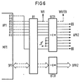
- FIG. 4 The variant shown in FIG. 4 is reproduced in the circuit arrangement.
- the branching of address port AP1 is indicated by dashed address lines.
- a register R1 is connected between the address bus isolator BT31 and the address port AP1. Both the address and the associated data from the data port DP1 of the first microprocessor are stored in this.
- the outputs of the register are connected to the address port APR2 and to the data port DPR2 via an address bus isolation stage BT21 and a data bus isolation stage BT31 (not shown in FIG. 4).
- Bit B5 is not required for addressing the second data memory, but merely indicates that data are present which are also to be written into the second data memory. If it is possible for the program to run, ie if the second microprocessor does not currently need its data memory, the bus isolators BT21, BT31 are switched through and the data can be written. Logical zeros are applied to the inputs B1 to B4 for the address bits B 1 to B 4 via the address bus isolating stages and the desired addressing is thus achieved.
- the address bit Bs is also connected to the address input B6 of the first data memory RAM1 (FIG. 5). As a result, the lower memory area is addressed, in which the data is stored which are simultaneously transferred to the second data memory.
- the addressing of the associated second data memory RAM2 by the second microprocessor MP2 has the special feature that the file areas are addressed via the second byte BY2 and the addressing within a file area takes place via the second byte.
- the file areas of the upper memory area of the data memory 1, into which data are written by the second microprocessor MP2, are also addressed via the second byte BY2.
- the selection KZU or SK is made via the least significant bit Bo of the first byte.
Landscapes
- Engineering & Computer Science (AREA)
- Computer Hardware Design (AREA)
- Theoretical Computer Science (AREA)
- Software Systems (AREA)
- Physics & Mathematics (AREA)
- General Engineering & Computer Science (AREA)
- General Physics & Mathematics (AREA)
- Exchange Systems With Centralized Control (AREA)
- Time-Division Multiplex Systems (AREA)
- Multi Processors (AREA)
Claims (6)
Priority Applications (1)
| Application Number | Priority Date | Filing Date | Title |
|---|---|---|---|
| AT86112521T ATE48324T1 (de) | 1985-09-20 | 1986-09-10 | Multi-mikroprozessorsystem mit zeitsparender adressierung von schreib-lese-speichern. |
Applications Claiming Priority (2)
| Application Number | Priority Date | Filing Date | Title |
|---|---|---|---|
| DE3533607 | 1985-09-20 | ||
| DE3533607 | 1985-09-20 |
Publications (2)
| Publication Number | Publication Date |
|---|---|
| EP0216253A1 EP0216253A1 (fr) | 1987-04-01 |
| EP0216253B1 true EP0216253B1 (fr) | 1989-11-29 |
Family
ID=6281513
Family Applications (1)
| Application Number | Title | Priority Date | Filing Date |
|---|---|---|---|
| EP86112521A Expired EP0216253B1 (fr) | 1985-09-20 | 1986-09-10 | Système multimicroprocesseur avec adressage de mémoires à lecture-écriture permettant une économie de temps |
Country Status (5)
| Country | Link |
|---|---|
| EP (1) | EP0216253B1 (fr) |
| AR (1) | AR241286A1 (fr) |
| AT (1) | ATE48324T1 (fr) |
| DE (1) | DE3667214D1 (fr) |
| GR (1) | GR862389B (fr) |
Families Citing this family (3)
| Publication number | Priority date | Publication date | Assignee | Title |
|---|---|---|---|---|
| FR2622711A1 (fr) * | 1987-11-04 | 1989-05-05 | Trt Telecom Radio Electr | Dispositif destine a remplacer un circuit integre comportant sur la meme puce un processeur de signal et un ensemble de memoire contenant des informations figees |
| JPH0433139A (ja) * | 1990-05-30 | 1992-02-04 | Fujitsu Ltd | ファィルアクセス方式 |
| JPH04149658A (ja) * | 1990-10-08 | 1992-05-22 | Canon Inc | 情報処理装置 |
Family Cites Families (1)
| Publication number | Priority date | Publication date | Assignee | Title |
|---|---|---|---|---|
| DE2713304A1 (de) * | 1977-03-25 | 1978-09-28 | Siemens Ag | Mehrrechnersystem |
-
1986
- 1986-09-10 DE DE8686112521T patent/DE3667214D1/de not_active Expired - Lifetime
- 1986-09-10 AT AT86112521T patent/ATE48324T1/de not_active IP Right Cessation
- 1986-09-10 EP EP86112521A patent/EP0216253B1/fr not_active Expired
- 1986-09-16 AR AR86305261A patent/AR241286A1/es active
- 1986-09-18 GR GR862389A patent/GR862389B/el unknown
Also Published As
| Publication number | Publication date |
|---|---|
| GR862389B (en) | 1987-01-16 |
| DE3667214D1 (de) | 1990-01-04 |
| EP0216253A1 (fr) | 1987-04-01 |
| AR241286A1 (es) | 1992-04-30 |
| ATE48324T1 (de) | 1989-12-15 |
Similar Documents
| Publication | Publication Date | Title |
|---|---|---|
| DE3232600C2 (fr) | ||
| DE3137627C1 (de) | Anordnung zur schnellen Nachrichtenuebertragung zwischen Rechnern | |
| DE2719247B2 (de) | Datenverarbeitungssystem | |
| DE2332734A1 (de) | Datenverarbeitungssystem | |
| WO2000007335A2 (fr) | Module de pontage | |
| DE2921419A1 (de) | Schaltungsanordnung und verfahren zur uebertragung digitaler information zwischen wenigstens einer ersten und einer zweiten sammelleitung | |
| EP0184706B1 (fr) | Montage d'interface | |
| DE2558417C3 (de) | Datenverarbeitungssystem | |
| EP0185260A2 (fr) | Interface pour le transfert direct d'informations | |
| EP0216253B1 (fr) | Système multimicroprocesseur avec adressage de mémoires à lecture-écriture permettant une économie de temps | |
| DE69016063T2 (de) | PCM-Übertragungssystem. | |
| EP0185936B1 (fr) | Montage de circuit d'interface pour la connexion de sources de données avec récepteurs de données et systèmes de commutation avec de tels montages de circuit d'interface | |
| EP0414950B1 (fr) | Méthode de commutation des informations transmises distributivement sur plusieurs tranches de temps | |
| DE69900032T2 (de) | Integrierte Schaltung mit mindestens zwei Speichern | |
| DE2714314C2 (de) | Datenverarbeitende Vorrichtung mit einem Datenspeicher | |
| EP0579845A1 (fr) | Réseau de couplages à étages parallèles à l'entrée pour carteaux numériques | |
| EP0027557A2 (fr) | Dispositif pour la transmission de signaux numériques entre des circuits d'émission et des circuits de réception travaillant avec différentes procédures de transmission de données et différents formats de données | |
| EP0215440B1 (fr) | Centre de traduction d'informations de signalisation d'un système de transmission multiplex à division temporelle | |
| EP0656736B1 (fr) | Méthode et appareil pour déterminer l'allocation du numéro de série d'une station radio mobile à des listes | |
| DE2252380C3 (de) | Datenverarbeitungsanordnung | |
| DE3109767A1 (de) | Zeitmultiplexkoppelfeldeinheit zur zeit-raum-vermittlung | |
| DE2837709C2 (de) | Schaltungsanordnung zur Behandlung von Teilwörtern in Rechnersystemen | |
| DE2047674C3 (de) | Fernmelde-, insbesondere Fernsprechvermittlungsanlage mit Zeitvielfachdurchschaltung | |
| DE3427026C2 (fr) | ||
| DE2555329C3 (de) | Steuereinrichtung aus mehreren Bausteinen für eine Vermittlungsanlage, insbesondere Fernsprechvermittlungsanlage, und Verfahren zum Betrieb der Steuereinrichtung |
Legal Events
| Date | Code | Title | Description |
|---|---|---|---|
| PUAI | Public reference made under article 153(3) epc to a published international application that has entered the european phase |
Free format text: ORIGINAL CODE: 0009012 |
|
| AK | Designated contracting states |
Kind code of ref document: A1 Designated state(s): AT BE CH DE FR GB IT LI NL SE |
|
| 17P | Request for examination filed |
Effective date: 19870424 |
|
| 17Q | First examination report despatched |
Effective date: 19890228 |
|
| GRAA | (expected) grant |
Free format text: ORIGINAL CODE: 0009210 |
|
| AK | Designated contracting states |
Kind code of ref document: B1 Designated state(s): AT BE CH DE FR GB IT LI NL SE |
|
| REF | Corresponds to: |
Ref document number: 48324 Country of ref document: AT Date of ref document: 19891215 Kind code of ref document: T |
|
| REF | Corresponds to: |
Ref document number: 3667214 Country of ref document: DE Date of ref document: 19900104 |
|
| ET | Fr: translation filed | ||
| ITF | It: translation for a ep patent filed | ||
| GBT | Gb: translation of ep patent filed (gb section 77(6)(a)/1977) | ||
| PLBE | No opposition filed within time limit |
Free format text: ORIGINAL CODE: 0009261 |
|
| PLBE | No opposition filed within time limit |
Free format text: ORIGINAL CODE: 0009261 |
|
| STAA | Information on the status of an ep patent application or granted ep patent |
Free format text: STATUS: NO OPPOSITION FILED WITHIN TIME LIMIT |
|
| 26N | No opposition filed | ||
| 26N | No opposition filed | ||
| ITTA | It: last paid annual fee | ||
| PGFP | Annual fee paid to national office [announced via postgrant information from national office to epo] |
Ref country code: GB Payment date: 19930816 Year of fee payment: 8 |
|
| PGFP | Annual fee paid to national office [announced via postgrant information from national office to epo] |
Ref country code: AT Payment date: 19930827 Year of fee payment: 8 |
|
| PGFP | Annual fee paid to national office [announced via postgrant information from national office to epo] |
Ref country code: SE Payment date: 19930914 Year of fee payment: 8 |
|
| PGFP | Annual fee paid to national office [announced via postgrant information from national office to epo] |
Ref country code: FR Payment date: 19930917 Year of fee payment: 8 |
|
| PGFP | Annual fee paid to national office [announced via postgrant information from national office to epo] |
Ref country code: BE Payment date: 19930920 Year of fee payment: 8 |
|
| PGFP | Annual fee paid to national office [announced via postgrant information from national office to epo] |
Ref country code: NL Payment date: 19930930 Year of fee payment: 8 |
|
| PGFP | Annual fee paid to national office [announced via postgrant information from national office to epo] |
Ref country code: CH Payment date: 19931215 Year of fee payment: 8 |
|
| PG25 | Lapsed in a contracting state [announced via postgrant information from national office to epo] |
Ref country code: GB Effective date: 19940910 Ref country code: AT Effective date: 19940910 |
|
| PG25 | Lapsed in a contracting state [announced via postgrant information from national office to epo] |
Ref country code: SE Effective date: 19940911 |
|
| PG25 | Lapsed in a contracting state [announced via postgrant information from national office to epo] |
Ref country code: LI Effective date: 19940930 Ref country code: CH Effective date: 19940930 Ref country code: BE Effective date: 19940930 |
|
| EAL | Se: european patent in force in sweden |
Ref document number: 86112521.9 |
|
| BERE | Be: lapsed |
Owner name: SIEMENS A.G. Effective date: 19940930 |
|
| PG25 | Lapsed in a contracting state [announced via postgrant information from national office to epo] |
Ref country code: NL Effective date: 19950401 |
|
| GBPC | Gb: european patent ceased through non-payment of renewal fee |
Effective date: 19940910 |
|
| NLV4 | Nl: lapsed or anulled due to non-payment of the annual fee | ||
| PG25 | Lapsed in a contracting state [announced via postgrant information from national office to epo] |
Ref country code: FR Effective date: 19950531 |
|
| REG | Reference to a national code |
Ref country code: CH Ref legal event code: PL |
|
| EUG | Se: european patent has lapsed |
Ref document number: 86112521.9 |
|
| REG | Reference to a national code |
Ref country code: FR Ref legal event code: ST |
|
| PGFP | Annual fee paid to national office [announced via postgrant information from national office to epo] |
Ref country code: DE Payment date: 19961118 Year of fee payment: 11 |
|
| PG25 | Lapsed in a contracting state [announced via postgrant information from national office to epo] |
Ref country code: DE Free format text: LAPSE BECAUSE OF NON-PAYMENT OF DUE FEES Effective date: 19980603 |
|
| PG25 | Lapsed in a contracting state [announced via postgrant information from national office to epo] |
Ref country code: IT Free format text: LAPSE BECAUSE OF NON-PAYMENT OF DUE FEES;WARNING: LAPSES OF ITALIAN PATENTS WITH EFFECTIVE DATE BEFORE 2007 MAY HAVE OCCURRED AT ANY TIME BEFORE 2007. THE CORRECT EFFECTIVE DATE MAY BE DIFFERENT FROM THE ONE RECORDED. Effective date: 20050910 |