EP0216603A2 - Appareil micro-onde générateur de post-luminescences plasmatiques - Google Patents
Appareil micro-onde générateur de post-luminescences plasmatiques Download PDFInfo
- Publication number
- EP0216603A2 EP0216603A2 EP86307178A EP86307178A EP0216603A2 EP 0216603 A2 EP0216603 A2 EP 0216603A2 EP 86307178 A EP86307178 A EP 86307178A EP 86307178 A EP86307178 A EP 86307178A EP 0216603 A2 EP0216603 A2 EP 0216603A2
- Authority
- EP
- European Patent Office
- Prior art keywords
- plasma
- process chamber
- workpiece
- resonant cavity
- electrodes
- Prior art date
- Legal status (The legal status is an assumption and is not a legal conclusion. Google has not performed a legal analysis and makes no representation as to the accuracy of the status listed.)
- Withdrawn
Links
Images

Classifications
-
- H—ELECTRICITY
- H01—ELECTRIC ELEMENTS
- H01J—ELECTRIC DISCHARGE TUBES OR DISCHARGE LAMPS
- H01J37/00—Discharge tubes with provision for introducing objects or material to be exposed to the discharge, e.g. for the purpose of examination or processing thereof
- H01J37/32—Gas-filled discharge tubes
- H01J37/32009—Arrangements for generation of plasma specially adapted for examination or treatment of objects, e.g. plasma sources
-
- G—PHYSICS
- G03—PHOTOGRAPHY; CINEMATOGRAPHY; ANALOGOUS TECHNIQUES USING WAVES OTHER THAN OPTICAL WAVES; ELECTROGRAPHY; HOLOGRAPHY
- G03F—PHOTOMECHANICAL PRODUCTION OF TEXTURED OR PATTERNED SURFACES, e.g. FOR PRINTING, FOR PROCESSING OF SEMICONDUCTOR DEVICES; MATERIALS THEREFOR; ORIGINALS THEREFOR; APPARATUS SPECIALLY ADAPTED THEREFOR
- G03F7/00—Photomechanical, e.g. photolithographic, production of textured or patterned surfaces, e.g. printing surfaces; Materials therefor, e.g. comprising photoresists; Apparatus specially adapted therefor
- G03F7/26—Processing photosensitive materials; Apparatus therefor
- G03F7/36—Imagewise removal not covered by groups G03F7/30 - G03F7/34, e.g. using gas streams, using plasma
-
- G—PHYSICS
- G03—PHOTOGRAPHY; CINEMATOGRAPHY; ANALOGOUS TECHNIQUES USING WAVES OTHER THAN OPTICAL WAVES; ELECTROGRAPHY; HOLOGRAPHY
- G03F—PHOTOMECHANICAL PRODUCTION OF TEXTURED OR PATTERNED SURFACES, e.g. FOR PRINTING, FOR PROCESSING OF SEMICONDUCTOR DEVICES; MATERIALS THEREFOR; ORIGINALS THEREFOR; APPARATUS SPECIALLY ADAPTED THEREFOR
- G03F7/00—Photomechanical, e.g. photolithographic, production of textured or patterned surfaces, e.g. printing surfaces; Materials therefor, e.g. comprising photoresists; Apparatus specially adapted therefor
- G03F7/26—Processing photosensitive materials; Apparatus therefor
- G03F7/42—Stripping or agents therefor
- G03F7/427—Stripping or agents therefor using plasma means only
-
- H—ELECTRICITY
- H01—ELECTRIC ELEMENTS
- H01J—ELECTRIC DISCHARGE TUBES OR DISCHARGE LAMPS
- H01J37/00—Discharge tubes with provision for introducing objects or material to be exposed to the discharge, e.g. for the purpose of examination or processing thereof
- H01J37/32—Gas-filled discharge tubes
- H01J37/32009—Arrangements for generation of plasma specially adapted for examination or treatment of objects, e.g. plasma sources
- H01J37/32082—Radio frequency generated discharge
-
- H—ELECTRICITY
- H01—ELECTRIC ELEMENTS
- H01J—ELECTRIC DISCHARGE TUBES OR DISCHARGE LAMPS
- H01J37/00—Discharge tubes with provision for introducing objects or material to be exposed to the discharge, e.g. for the purpose of examination or processing thereof
- H01J37/32—Gas-filled discharge tubes
- H01J37/32009—Arrangements for generation of plasma specially adapted for examination or treatment of objects, e.g. plasma sources
- H01J37/32192—Microwave generated discharge
- H01J37/32211—Means for coupling power to the plasma
- H01J37/32247—Resonators
-
- H—ELECTRICITY
- H01—ELECTRIC ELEMENTS
- H01J—ELECTRIC DISCHARGE TUBES OR DISCHARGE LAMPS
- H01J37/00—Discharge tubes with provision for introducing objects or material to be exposed to the discharge, e.g. for the purpose of examination or processing thereof
- H01J37/32—Gas-filled discharge tubes
- H01J37/32009—Arrangements for generation of plasma specially adapted for examination or treatment of objects, e.g. plasma sources
- H01J37/32357—Generation remote from the workpiece, e.g. down-stream
Definitions
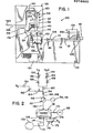
- an apparatus for treating a workpiece by a plasma formed from a gas comprising a resonant cavity having a longitudinal axis, transporting means extending through said resonant cavity for transporting a gas therethrough from a source thereof, said transporting means including a linear portion arranged substantially parallel to said longitudinal axis of said resonant cavity, a source of energy coupled to said resonant cavity for generating a plasma from said gas within said transporting means, and a process chamber arranged in fluid communication with said transporting means for receiving a workpiece to be treated by said plasma.
- the microwave plasma tube 140 is fully movable in a vertical direction relative to the waveguide resonant cavity 138 and power supply 134 along its longitudinal axis upon movement of the chamber cover 122 of the stripping/etching chamber 118 during the opening and closing thereof.
- the vertical movement of the microwave plasma tube 140 is permitted by the coupling of its upper extending end to the rigid pipe 1 4 6 by means of the flexible pipe 144.
- vertical movement of the microwave plasma tube 140 is stabilized by the bearing block 142.
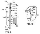
- the microwave reactor 137 is further provided with a pair of spaced-apart fine tuning screws 148 and a mercury/argon plasma ignitor 150 supported within a holder 152 attached adjacent the upper end of the waveguide resonant cavity 138.
- a known characteristic of microwave plasmas is that the microwave energy must be coupled to the plasma through a resonant cavity, i.e., waveguide resonant cavity 138.
- the resonant cavity produces a high density electric field which ionizes the contained gas, forming the plasma.
- Many types of cavities have been proposed and are in use to generate plasmas.
- the known resonant cavities are more suited for laboratory production of plasmas rather than for industrial application.
- these known laboratory resonant cavities are complex in design, difficult to tune, and provide inefficient coupling of microwave energy to the plasma.
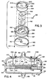
- the quartz tube 250 may be extended through the opening 248 and into the interior of the waveguide resonant cavity 138.
- the microwave energy supplied in the waveguide resonant cavity 138 will efficiently couple to the quartz tube and create a plasma from the contained mercury and argon which, in turn, will emit ultraviolet light.
- the intense ultraviolet light emission from the quartz tube 250 will, as described, ignite a plasma in the adjacent microwave plasma tube 140.
- This embodiment provides a passive mercury/argon plasma ignitor 150 having a high degree of reliability.
Landscapes
- Physics & Mathematics (AREA)
- Engineering & Computer Science (AREA)
- Plasma & Fusion (AREA)
- Chemical & Material Sciences (AREA)
- Analytical Chemistry (AREA)
- General Physics & Mathematics (AREA)
- Drying Of Semiconductors (AREA)
- Treatment Of Fiber Materials (AREA)
- ing And Chemical Polishing (AREA)
Applications Claiming Priority (2)
| Application Number | Priority Date | Filing Date | Title |
|---|---|---|---|
| US06/777,032 US4673456A (en) | 1985-09-17 | 1985-09-17 | Microwave apparatus for generating plasma afterglows |
| US777032 | 1991-10-16 |
Publications (2)
| Publication Number | Publication Date |
|---|---|
| EP0216603A2 true EP0216603A2 (fr) | 1987-04-01 |
| EP0216603A3 EP0216603A3 (fr) | 1987-12-23 |
Family
ID=25109076
Family Applications (1)
| Application Number | Title | Priority Date | Filing Date |
|---|---|---|---|
| EP86307178A Withdrawn EP0216603A3 (fr) | 1985-09-17 | 1986-09-17 | Appareil micro-onde générateur de post-luminescences plasmatiques |
Country Status (4)
| Country | Link |
|---|---|
| US (1) | US4673456A (fr) |
| EP (1) | EP0216603A3 (fr) |
| JP (1) | JPS62109986A (fr) |
| CA (1) | CA1269719A (fr) |
Cited By (5)
| Publication number | Priority date | Publication date | Assignee | Title |
|---|---|---|---|---|
| EP0234387A3 (en) * | 1986-02-14 | 1989-02-01 | Fujitsu Limited | Method of removing photoresist on a semiconductor wafer |
| EP0474244A3 (fr) * | 1990-09-07 | 1992-04-01 | Tokyo Electron Limited | Méthode de traitement par plasma |
| EP0665306A1 (fr) * | 1994-01-19 | 1995-08-02 | TOKYO ELECTRON AMERICA Inc. | Procédé et dispositif d'allumage d'un plasma dans un module de traitement |
| EP0305946B1 (fr) * | 1987-08-28 | 1996-10-30 | Kabushiki Kaisha Toshiba | Procédé d'enlèvement de films organique et/ou minéraux par plasma |
| US5773201A (en) * | 1987-08-19 | 1998-06-30 | Fujitsu Limited | Method of stripping a resist mask |
Families Citing this family (74)
| Publication number | Priority date | Publication date | Assignee | Title |
|---|---|---|---|---|
| US4718974A (en) * | 1987-01-09 | 1988-01-12 | Ultraphase Equipment, Inc. | Photoresist stripping apparatus using microwave pumped ultraviolet lamp |
| US4776923A (en) * | 1987-01-20 | 1988-10-11 | Machine Technology, Inc. | Plasma product treatment apparatus and methods and gas transport systems for use therein |
| US4971856A (en) * | 1987-05-07 | 1990-11-20 | Arthur Karp | Microwave components with a surface coating which imparts a very high RF loss |
| US4872938A (en) * | 1987-07-16 | 1989-10-10 | Texas Instruments Incorporated | Processing apparatus |
| US4818326A (en) * | 1987-07-16 | 1989-04-04 | Texas Instruments Incorporated | Processing apparatus |
| US4867841A (en) * | 1987-07-16 | 1989-09-19 | Texas Instruments Incorporated | Method for etch of polysilicon film |
| US4891488A (en) * | 1987-07-16 | 1990-01-02 | Texas Instruments Incorporated | Processing apparatus and method |
| US4904621A (en) * | 1987-07-16 | 1990-02-27 | Texas Instruments Incorporated | Remote plasma generation process using a two-stage showerhead |
| US4832779A (en) * | 1987-07-16 | 1989-05-23 | Texas Instruments Incorporated | Processing apparatus |
| US4844773A (en) * | 1987-07-16 | 1989-07-04 | Texas Instruments Incorporated | Process for etching silicon nitride film |
| US4832778A (en) * | 1987-07-16 | 1989-05-23 | Texas Instruments Inc. | Processing apparatus for wafers |
| US4838984A (en) * | 1987-07-16 | 1989-06-13 | Texas Instruments Incorporated | Method for etching films of mercury-cadmium-telluride and zinc sulfid |
| US4842687A (en) * | 1987-07-16 | 1989-06-27 | Texas Instruments Incorporated | Method for etching tungsten |
| US4878994A (en) * | 1987-07-16 | 1989-11-07 | Texas Instruments Incorporated | Method for etching titanium nitride local interconnects |
| US4830705A (en) * | 1987-07-16 | 1989-05-16 | Texas Instruments Incorporated | Method for etch of GaAs |
| US4837113A (en) * | 1987-07-16 | 1989-06-06 | Texas Instruments Incorporated | Method for depositing compound from group II-VI |
| US4863558A (en) * | 1987-07-16 | 1989-09-05 | Texas Instruments Incorporated | Method for etching tungsten |
| US4910043A (en) * | 1987-07-16 | 1990-03-20 | Texas Instruments Incorporated | Processing apparatus and method |
| US4849067A (en) * | 1987-07-16 | 1989-07-18 | Texas Instruments Incorporated | Method for etching tungsten |
| US4842676A (en) * | 1987-07-16 | 1989-06-27 | Texas Instruments Incorporated | Process for etch of tungsten |
| US4838990A (en) * | 1987-07-16 | 1989-06-13 | Texas Instruments Incorporated | Method for plasma etching tungsten |
| US4832777A (en) * | 1987-07-16 | 1989-05-23 | Texas Instruments Incorporated | Processing apparatus and method |
| US4816098A (en) * | 1987-07-16 | 1989-03-28 | Texas Instruments Incorporated | Apparatus for transferring workpieces |
| US4874723A (en) * | 1987-07-16 | 1989-10-17 | Texas Instruments Incorporated | Selective etching of tungsten by remote and in situ plasma generation |
| US4828649A (en) * | 1987-07-16 | 1989-05-09 | Texas Instruments Incorporated | Method for etching an aluminum film doped with silicon |
| US4820377A (en) * | 1987-07-16 | 1989-04-11 | Texas Instruments Incorporated | Method for cleanup processing chamber and vacuum process module |
| US4877757A (en) * | 1987-07-16 | 1989-10-31 | Texas Instruments Incorporated | Method of sequential cleaning and passivating a GaAs substrate using remote oxygen plasma |
| US4857132A (en) * | 1987-07-16 | 1989-08-15 | Texas Instruments Incorporated | Processing apparatus for wafers |
| US4830700A (en) * | 1987-07-16 | 1989-05-16 | Texas Instruments Incorporated | Processing apparatus and method |
| US4855160A (en) * | 1987-07-16 | 1989-08-08 | Texas Instruments Incorporated | Method for passivating wafer |
| US4822450A (en) * | 1987-07-16 | 1989-04-18 | Texas Instruments Incorporated | Processing apparatus and method |
| US4855016A (en) * | 1987-07-16 | 1989-08-08 | Texas Instruments Incorporated | Method for etching aluminum film doped with copper |
| US4842686A (en) * | 1987-07-17 | 1989-06-27 | Texas Instruments Incorporated | Wafer processing apparatus and method |
| US4836902A (en) * | 1987-10-09 | 1989-06-06 | Northern Telecom Limited | Method and apparatus for removing coating from substrate |
| US4859303A (en) * | 1987-10-09 | 1989-08-22 | Northern Telecom Limited | Method and apparatus for removing coating from substrate |
| US5310703A (en) * | 1987-12-01 | 1994-05-10 | U.S. Philips Corporation | Method of manufacturing a semiconductor device, in which photoresist on a silicon oxide layer on a semiconductor substrate is stripped using an oxygen plasma afterglow and a biased substrate |
| US4988533A (en) * | 1988-05-27 | 1991-01-29 | Texas Instruments Incorporated | Method for deposition of silicon oxide on a wafer |
| US4961820A (en) * | 1988-06-09 | 1990-10-09 | Fujitsu Limited | Ashing method for removing an organic film on a substance of a semiconductor device under fabrication |
| DE3834984A1 (de) * | 1988-10-14 | 1990-04-19 | Leybold Ag | Einrichtung zur erzeugung von elektrisch geladenen und/oder ungeladenen teilchen |
| US4869777A (en) * | 1988-12-16 | 1989-09-26 | Ibm Corporation | Method for selectively etching the materials of a composite of two materials |
| US4888088A (en) * | 1989-03-06 | 1989-12-19 | Tegal Corporation | Ignitor for a microwave sustained plasma |
| EP0418540A3 (en) * | 1989-08-11 | 1991-08-07 | Sanyo Electric Co., Ltd. | Dry etching method |
| US4946549A (en) * | 1989-10-27 | 1990-08-07 | At&T Bell Laboratories | Method for fabricating or modifying an article comprising the removal of a polymer coating |
| JP2602336B2 (ja) * | 1989-11-29 | 1997-04-23 | 株式会社日立製作所 | プラズマ処理装置 |
| US5198634A (en) * | 1990-05-21 | 1993-03-30 | Mattson Brad S | Plasma contamination removal process |
| DE4117005C2 (de) * | 1990-06-11 | 2003-07-24 | Tokyo Electron Ltd | Verfahren und Anordnung zum Einwirken mit einem Lichtstrahl in einen Entladungsraum |
| JP3375646B2 (ja) * | 1991-05-31 | 2003-02-10 | 株式会社日立製作所 | プラズマ処理装置 |
| US6046425A (en) * | 1991-05-31 | 2000-04-04 | Hitachi, Ltd. | Plasma processing apparatus having insulator disposed on inner surface of plasma generating chamber |
| US5273587A (en) * | 1992-09-04 | 1993-12-28 | United Solar Systems Corporation | Igniter for microwave energized plasma processing apparatus |
| JPH08186098A (ja) * | 1994-12-27 | 1996-07-16 | Ryoden Semiconductor Syst Eng Kk | 感光性樹脂の除去方法および除去装置 |
| US5702530A (en) * | 1995-06-23 | 1997-12-30 | Applied Materials, Inc. | Distributed microwave plasma reactor for semiconductor processing |
| JPH0936103A (ja) * | 1995-07-18 | 1997-02-07 | Ulvac Japan Ltd | 半導体ウェハのエッチング及びレジスト除去のための方法並びに装置 |
| US5780359A (en) * | 1995-12-11 | 1998-07-14 | Applied Materials, Inc. | Polymer removal from top surfaces and sidewalls of a semiconductor wafer |
| US5824604A (en) * | 1996-01-23 | 1998-10-20 | Mattson Technology, Inc. | Hydrocarbon-enhanced dry stripping of photoresist |
| US5882489A (en) * | 1996-04-26 | 1999-03-16 | Ulvac Technologies, Inc. | Processes for cleaning and stripping photoresist from surfaces of semiconductor wafers |
| US6015761A (en) * | 1996-06-26 | 2000-01-18 | Applied Materials, Inc. | Microwave-activated etching of dielectric layers |
| US5795831A (en) * | 1996-10-16 | 1998-08-18 | Ulvac Technologies, Inc. | Cold processes for cleaning and stripping photoresist from surfaces of semiconductor wafers |
| JP3916284B2 (ja) | 1997-02-28 | 2007-05-16 | 東京応化工業株式会社 | 多層配線構造の形成方法 |
| JP3394263B2 (ja) * | 1997-04-28 | 2003-04-07 | 芝浦メカトロニクス株式会社 | 真空処理方法及び装置 |
| US6379576B2 (en) | 1997-11-17 | 2002-04-30 | Mattson Technology, Inc. | Systems and methods for variable mode plasma enhanced processing of semiconductor wafers |
| US6080680A (en) * | 1997-12-19 | 2000-06-27 | Lam Research Corporation | Method and composition for dry etching in semiconductor fabrication |
| US6432830B1 (en) * | 1998-05-15 | 2002-08-13 | Applied Materials, Inc. | Semiconductor fabrication process |
| JP2000077410A (ja) | 1998-08-27 | 2000-03-14 | Tokyo Ohka Kogyo Co Ltd | 多層配線構造の形成方法 |
| US6900138B1 (en) * | 1999-03-01 | 2005-05-31 | Micron Technology, Inc. | Oxygen plasma treatment for nitride surface to reduce photo footing |
| RU2216818C1 (ru) * | 2003-01-28 | 2003-11-20 | Общество с ограниченной ответственностью "ЭпиЛаб" | Эцр-плазменный источник для обработки полупроводниковых структур, способ обработки полупроводниковых структур, способ изготовления полупроводниковых приборов и интегральных схем (варианты), полупроводниковый прибор или интегральная схема (варианты) |
| KR100555620B1 (ko) * | 2003-10-28 | 2006-03-03 | 주식회사 디엠에스 | 기판 운반시스템 및 운반방법 |
| JP4628807B2 (ja) * | 2005-01-28 | 2011-02-09 | 株式会社日立ハイテクノロジーズ | 真空処理装置および真空処理方法 |
| US20070054447A1 (en) * | 2005-09-07 | 2007-03-08 | Hsin Tai | Multistep etching method |
| US7687303B1 (en) * | 2005-11-01 | 2010-03-30 | Mentor Graphics Corporation | Method for determining via/contact pattern density effect in via/contact etch rate |
| US20080163817A1 (en) * | 2007-01-04 | 2008-07-10 | Oc Oerlikon Balzers Ag | Apparatus for gas handling in vacuum processes |
| US20160121418A1 (en) * | 2012-01-25 | 2016-05-05 | Gordon Hanka | Welder Powered Arc Starter |
| US20150118855A1 (en) * | 2013-10-30 | 2015-04-30 | Nisene Technology Group | Microwave induced plasma decapsulation |
| JP2015138669A (ja) * | 2014-01-22 | 2015-07-30 | パナソニックIpマネジメント株式会社 | 照明装置および点灯回路 |
| ES2696227B2 (es) * | 2018-07-10 | 2019-06-12 | Centro De Investig Energeticas Medioambientales Y Tecnologicas Ciemat | Fuente de iones interna para ciclotrones de baja erosion |
Family Cites Families (24)
| Publication number | Priority date | Publication date | Assignee | Title |
|---|---|---|---|---|
| US4192706A (en) * | 1975-01-22 | 1980-03-11 | Tokyo Shibaura Electric Co., Ltd. | Gas-etching device |
| JPS5211175A (en) * | 1975-07-18 | 1977-01-27 | Toshiba Corp | Activated gas reacting apparatus |
| US4115184A (en) * | 1975-12-29 | 1978-09-19 | Northern Telecom Limited | Method of plasma etching |
| JPS5291650A (en) * | 1976-01-29 | 1977-08-02 | Toshiba Corp | Continuous gas plasma etching apparatus |
| US4138306A (en) * | 1976-08-31 | 1979-02-06 | Tokyo Shibaura Electric Co., Ltd. | Apparatus for the treatment of semiconductors |
| JPS5329076A (en) * | 1976-08-31 | 1978-03-17 | Toshiba Corp | Plasma treating apparatus of semiconductor substrates |
| JPS53121469A (en) * | 1977-03-31 | 1978-10-23 | Toshiba Corp | Gas etching unit |
| US4230515A (en) * | 1978-07-27 | 1980-10-28 | Davis & Wilder, Inc. | Plasma etching apparatus |
| US4253907A (en) * | 1979-03-28 | 1981-03-03 | Western Electric Company, Inc. | Anisotropic plasma etching |
| FR2463975A1 (fr) * | 1979-08-22 | 1981-02-27 | Onera (Off Nat Aerospatiale) | Procede et appareil pour la gravure chimique par voie seche des circuits integres |
| US4282267A (en) * | 1979-09-20 | 1981-08-04 | Western Electric Co., Inc. | Methods and apparatus for generating plasmas |
| JPS5813625B2 (ja) * | 1979-12-12 | 1983-03-15 | 超エル・エス・アイ技術研究組合 | ガスプラズマ食刻法 |
| US4328068A (en) * | 1980-07-22 | 1982-05-04 | Rca Corporation | Method for end point detection in a plasma etching process |
| US4342901A (en) * | 1980-08-11 | 1982-08-03 | Eaton Corporation | Plasma etching electrode |
| US4340462A (en) * | 1981-02-13 | 1982-07-20 | Lam Research Corporation | Adjustable electrode plasma processing chamber |
| US4368092A (en) * | 1981-04-02 | 1983-01-11 | The Perkin-Elmer Corporation | Apparatus for the etching for semiconductor devices |
| US4431898A (en) * | 1981-09-01 | 1984-02-14 | The Perkin-Elmer Corporation | Inductively coupled discharge for plasma etching and resist stripping |
| US4392932A (en) * | 1981-11-12 | 1983-07-12 | Varian Associates, Inc. | Method for obtaining uniform etch by modulating bias on extension member around radio frequency etch table |
| US4512283A (en) * | 1982-02-01 | 1985-04-23 | Texas Instruments Incorporated | Plasma reactor sidewall shield |
| US4507588A (en) * | 1983-02-28 | 1985-03-26 | Board Of Trustees Operating Michigan State University | Ion generating apparatus and method for the use thereof |
| JPS59163826A (ja) * | 1983-03-08 | 1984-09-14 | Toshiba Corp | ドライエツチング方法 |
| JPS6016424A (ja) * | 1983-07-08 | 1985-01-28 | Fujitsu Ltd | マイクロ波プラズマ処理方法及びその装置 |
| JPH0626199B2 (ja) * | 1983-12-14 | 1994-04-06 | 株式会社日立製作所 | エッチング方法 |
| US4581100A (en) * | 1984-10-29 | 1986-04-08 | International Business Machines Corporation | Mixed excitation plasma etching system |
-
1985
- 1985-09-17 US US06/777,032 patent/US4673456A/en not_active Expired - Lifetime
-
1986
- 1986-09-09 CA CA000517825A patent/CA1269719A/fr not_active Expired - Fee Related
- 1986-09-17 EP EP86307178A patent/EP0216603A3/fr not_active Withdrawn
- 1986-09-17 JP JP61219108A patent/JPS62109986A/ja active Pending
Cited By (11)
| Publication number | Priority date | Publication date | Assignee | Title |
|---|---|---|---|---|
| EP0234387A3 (en) * | 1986-02-14 | 1989-02-01 | Fujitsu Limited | Method of removing photoresist on a semiconductor wafer |
| US4938839A (en) * | 1986-02-14 | 1990-07-03 | Fujitsu Limited | Method of removing photoresist on a semiconductor wafer |
| US5773201A (en) * | 1987-08-19 | 1998-06-30 | Fujitsu Limited | Method of stripping a resist mask |
| US5961775A (en) * | 1987-08-19 | 1999-10-05 | Fujitsu Limited | Apparatus for removing organic resist from semiconductor |
| US5998104A (en) * | 1987-08-19 | 1999-12-07 | Fujitsu Limited | Method of stripping a resist mask |
| EP0305946B1 (fr) * | 1987-08-28 | 1996-10-30 | Kabushiki Kaisha Toshiba | Procédé d'enlèvement de films organique et/ou minéraux par plasma |
| EP0474244A3 (fr) * | 1990-09-07 | 1992-04-01 | Tokyo Electron Limited | Méthode de traitement par plasma |
| US5246529A (en) * | 1990-09-07 | 1993-09-21 | Tokyo Electron Limited | Plasma processing method |
| EP0665306A1 (fr) * | 1994-01-19 | 1995-08-02 | TOKYO ELECTRON AMERICA Inc. | Procédé et dispositif d'allumage d'un plasma dans un module de traitement |
| US5565036A (en) * | 1994-01-19 | 1996-10-15 | Tel America, Inc. | Apparatus and method for igniting plasma in a process module |
| US5789867A (en) * | 1994-01-19 | 1998-08-04 | Tel America, Inc. | Apparatus and method for igniting plasma in a process module |
Also Published As
| Publication number | Publication date |
|---|---|
| JPS62109986A (ja) | 1987-05-21 |
| US4673456A (en) | 1987-06-16 |
| EP0216603A3 (fr) | 1987-12-23 |
| CA1269719A (fr) | 1990-05-29 |
Similar Documents
| Publication | Publication Date | Title |
|---|---|---|
| US4673456A (en) | Microwave apparatus for generating plasma afterglows | |
| US4689112A (en) | Method and apparatus for dry processing of substrates | |
| US4148705A (en) | Gas plasma reactor and process | |
| US5707485A (en) | Method and apparatus for facilitating removal of material from the backside of wafers via a plasma etch | |
| US4699689A (en) | Method and apparatus for dry processing of substrates | |
| US4540466A (en) | Method of fabricating semiconductor device by dry process utilizing photochemical reaction, and apparatus therefor | |
| US4987284A (en) | Downstream microwave plasma processing apparatus having an improved coupling structure between microwave plasma | |
| US4822450A (en) | Processing apparatus and method | |
| US6761796B2 (en) | Method and apparatus for micro-jet enabled, low-energy ion generation transport in plasma processing | |
| US5198634A (en) | Plasma contamination removal process | |
| US4828649A (en) | Method for etching an aluminum film doped with silicon | |
| EP0234387B1 (fr) | Procédé d'élimination d'une photoréserve sur une plaquette semi-conductrice | |
| US20070051471A1 (en) | Methods and apparatus for stripping | |
| US20030213561A1 (en) | Atmospheric pressure plasma processing reactor | |
| JPS61107730A (ja) | 複合励起プラズマ・エツチング・システム | |
| KR20040105567A (ko) | 유기층 제거 방법 및 장치 | |
| EP0474244B1 (fr) | Méthode de traitement par plasma | |
| US4915777A (en) | Method for etching tungsten | |
| KR20000075467A (ko) | 폴리카보네이트 에칭 마스크를 이용하는 플라즈마 에칭 방법 | |
| US4736087A (en) | Plasma stripper with multiple contact point cathode | |
| US6960533B2 (en) | Method of processing a sample surface having a masking material and an anti-reflective film using a plasma | |
| US4820378A (en) | Process for etching silicon nitride selectively to silicon oxide | |
| JPH0936103A (ja) | 半導体ウェハのエッチング及びレジスト除去のための方法並びに装置 | |
| US20130160793A1 (en) | Plasma generating apparatus and process for simultaneous exposure of a workpiece to electromagnetic radiation and plasma | |
| JP2005064120A (ja) | プラズマ処理装置およびプラズマ処理方法 |
Legal Events
| Date | Code | Title | Description |
|---|---|---|---|
| PUAI | Public reference made under article 153(3) epc to a published international application that has entered the european phase |
Free format text: ORIGINAL CODE: 0009012 |
|
| AK | Designated contracting states |
Kind code of ref document: A2 Designated state(s): AT BE CH DE FR GB IT LI LU NL SE |
|
| PUAL | Search report despatched |
Free format text: ORIGINAL CODE: 0009013 |
|
| AK | Designated contracting states |
Kind code of ref document: A3 Designated state(s): AT BE CH DE FR GB IT LI LU NL SE |
|
| 17P | Request for examination filed |
Effective date: 19880202 |
|
| 17Q | First examination report despatched |
Effective date: 19890221 |
|
| STAA | Information on the status of an ep patent application or granted ep patent |
Free format text: STATUS: THE APPLICATION IS DEEMED TO BE WITHDRAWN |
|
| 18D | Application deemed to be withdrawn |
Effective date: 19890905 |
|
| RIN1 | Information on inventor provided before grant (corrected) |
Inventor name: LINXWILER, KENNETH ELGIN Inventor name: HOFF, ANDREW MILLARD Inventor name: SPENCER, JOHN EDWARD Inventor name: BOREL, RICHARD ALAN |