EP0216700A2 - Maskengenerierungssystem für Vektorprozessor - Google Patents
Maskengenerierungssystem für Vektorprozessor Download PDFInfo
- Publication number
- EP0216700A2 EP0216700A2 EP86402028A EP86402028A EP0216700A2 EP 0216700 A2 EP0216700 A2 EP 0216700A2 EP 86402028 A EP86402028 A EP 86402028A EP 86402028 A EP86402028 A EP 86402028A EP 0216700 A2 EP0216700 A2 EP 0216700A2
- Authority
- EP
- European Patent Office
- Prior art keywords
- register
- mask
- elements
- vector
- pattern
- Prior art date
- Legal status (The legal status is an assumption and is not a legal conclusion. Google has not performed a legal analysis and makes no representation as to the accuracy of the status listed.)
- Withdrawn
Links
Images


Classifications
-
- G—PHYSICS
- G06—COMPUTING OR CALCULATING; COUNTING
- G06F—ELECTRIC DIGITAL DATA PROCESSING
- G06F15/00—Digital computers in general; Data processing equipment in general
- G06F15/76—Architectures of general purpose stored program computers
- G06F15/80—Architectures of general purpose stored program computers comprising an array of processing units with common control, e.g. single instruction multiple data processors
- G06F15/8053—Vector processors
- G06F15/8076—Details on data register access
- G06F15/8084—Special arrangements thereof, e.g. mask or switch
Definitions
- the present invention relates to a system for generating a mask pattern for a mask register (MR) in a vector data processing apparatus, for use in a supercomputer, having a calculational mask function by means of the mask register.
- MR mask register
- vector processors that is, supercomputers
- FFT fast Fourier transformation
- VGM mask pattern generation instruction
- MR mask register
- R2I the value at the R2 portion of the instruction
- COMP complement number generating circuit
- a definite number, for example, "l” from a constant circuit (CNST) 2 and a complement of l in the above-mentioned R2I are added, so a definite number "l” is subtracted from said R2I.
- the output of a decoder (VGM) 4 and a modifier (MI) designated by said VGM instruction execute an exclusive OR operation in an exclusive OR circuit XOR, to store the result in the head element of mask registor (MR) which is assigned by the VGM instruction.
- MI modifier
- the output of the decoder VGM is "0", and functions so that "000---0” or "lll---l” is stored into the mask register MR till the vector length (VL).
- FIG. 3A and 3B The example of a mask pattern so generated is shown in Figs. 3A and 3B.
- a mask pattern which is necessary to the vector operation as shown in Figs. 4A and 4B, first, a plurality of vector instructions and scalar instructions were necessary, and second, mask pattern is stored in the memory in advance and must be loaded into the mask register (MR) from said memory every time it is needed.
- MR mask register
- the next vector generation series (VGS) instruction (IV) creates an arithmetical progression which represents the content (in this example "l") of the general-purpose register (GRl) in the vector register (VRl). That is, in this example, a progression VRl: l, 2, 3, 4, ---, VL is stored therein.
- VNM vector and mask
- MR3 mask register
- the system comprising: designation means for designating sequential "i” elements of "0” or “l” from the beginning element of the mask register and the subsequent sequential "j” elements of "l” or “0”; and control means for rendering the "i” elements to be “0” or “l”, the “j” elements to be “l” or “0”, and the remaining entire elements to be all “0's” or all “l's", when "i” plus “j” is smaller than a vector length VL which is the object of calculation of a vector data operand used in a vector instruction; a desired mask pattern of "0” or “l” being able to
- the system comprising: designation means for designating sequential "i” elements of "0” or “l” from the beginning element of the mask register and the subsequent sequential "j” elements of "l” or “0”; and control means for instructing the repeat "i” elements of "0” or “l” and “j” elements of "l” or “0” until a vector length which is the object of calculation of a vector data operand used in a vector instruction is attained, when "i” plus "j” is smaller than the above-mentioned vector length; desired mask patterns including repetitive patterns being able to be generated in the mask register.
- FIG. 7 is a block diagram showing an embodiment in accordance with the present invention.
- an instruction means for generating a mask pattern with a vector period or specified means therefore, wherein sequential i elements of "0" or “l” are stored in a head element of a mask register MR, then successively, the sequential j elements of "l” or “0” are stored and the remaining entire elements of all “0” or all “l” are stored, or in order to generate a mask pattern which repeats the above-mentioned (i + j) elements of "0" or "l” combination pattern until a vector length is attained.
- VGMZ a mask pattern for vector periods
- register (R2I) l3 which, after executing the instruction, sets the i contents of R2 portion in the above-mentioned instruction, a register ⁇ (R2+l)I ⁇ l4 which sets the j contents of the R2 portion plus l in the above-mentioned instruction, a register (AR) 23 which, when at the starting time of execution of the above-described VGMZ instruction, is "0" and then when the VGMZ control portion l5 detects the later event variation, inverts the initial value, and a register (PMWR) 22 which, after the modifier portion MI of the VGMZ instruction has been initialized, the setting of the output of exclusive OR circuit (XOR) 24 is repeated.
- R2I register
- the VGMZ control portion l5 recognizes that an event variation has occurred and sets the aforementioned register (AR) 23 to "l” and the calculation of an exclusive OR is carried out by the register (PMWR) 22 and the exclusive OR circuit (XOR) 24, and the system functions to store "l” in the corresponding elements of the mask register (MR).
- MI modifier
- the content (designating the above-mentioned j elements) of the register ⁇ (R2+l)I ⁇ l4 is input into the mask pipeline adder (MP ADDER) 32, and as a result of the same subtraction processing, the system is so constituted that i elements of "0" and j elements of "l" are stored in the mask register (MR).
- gate means 3l will be provided for repeating the above-mentioned (i+j) elements of 0/l pattern as a fundamental pattern till the vector length (VL).
- the vector data processor having at least a mask register (MR) and a vector register (VR) to enable executing the so-called calculation mask function in which, when the value of the mask register (MR) is "l" responsive to a respective element of the vector register (VR), a calculation is executed for the corresponding element of the vector register (VR), while when the value of the mask register is "0", a calculation is not executed, there is provided an instruction means for generating a mask periodic pattern for a vector (VGMZ) or other means, wherein in the mask register MR which a first operand Rl of said instruction designates, "0" is written into the elements A of the element number 0 to the numbers denoted by the second operand R2 minus l, while “l” is written into the elements B of the element number denoted by the second operand R2 to 'the number denoted by the operand of the second operand R2 plus l' minus l, and further, the mask pattern is generated repetitively as long as the elements denoted by, for
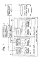
- Figure l is a schematic block diagram of a vector data processing apparatus to which the present invention is to be applied.
- the vector data processing apparatus is composed of a mainstorage unit “MSU” 6, a memory control unit “MCU” 7, a processor unit 5, an input/output processor “IOP” 8l and a direct access storage device “DASD” 82.
- MSU mainstorage unit
- MCU memory control unit
- IOP input/output processor
- DASD direct access storage device
- the processor unit 5 is composed of a vector unit 5l and a scalar unit 52.
- the vector unit 5l is composed of a mask register "MR" 5ll connected to the memory control unit 7, a vector register "VR" 5l2 connected also to the memory control unit 7, an adder 5l3 which receives two outputs of the vector register 5l2 and the output of addition is delivered to the vector register 5l2 and a multiplier 5l4 which receives two outputs of the vector register 5l2 and the output of multiplication is delivered to the vector register 5l2.
- the scalar unit 52 is composed of a cache 5l2 which means a unit of fast coordinate-addressable storage to hold data with high access probability, an adder 522 which receives two outputs of the cache 52l and the output of addition is returned to the cache 52l and a multiplier 523 which receives two outputs of the cache 52l and the output of multiplication is returned to the cache 52l.
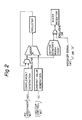
- FIG. 7 is a block diagram of a vector data processing apparatus according to an embodiment of the present invention.
- Functional blocks requisite for executing the present invention are a VGMZ control portion l5, a Register (AR) 23, a Register (PMWR) 22, amd an Exclusive OR circuit (XOR) 24.
- FIG. 5 An example of a format of an instruction for generating a periodical mask pattern necessary for the present invention will be designated in Figure 5. Due to this VGMZ instruction, a plurality of "0"s are stored in a mask register MR denoted by the Rl portion from the head element to the element number minus l shown by a general-purpose register denoted by the R2 portion while a plurality of "l"s are stored therein from the element code shown by the general-purpose register denote by the R2 portion, to the element code minus l shown by the general-purpose register denoted by (R2+l).
- the content of the general-purpose register designated by the above-mentioned portion "R2" and the content of the general-purpose register designated by the portion “R2+l” are set in a register “R2I” l3 and a register “(R2+l)I” l4, respectively and as well as in the VGMZ control portion l5, a register "AR" 23 is set to "0".
- the value of the above-mentioned MI portion is set to a register PMWR 22 by means of a start bit not shown in the figure, to initialize the registers R2I, (R2+l)I and PMWR.
- an exclusive OR value of the content of the above-mentioned register "AR" 23 and of the content of the register “PMWR” 22 is calculated by an exclusive OR (hereinafter referred to as XOR) circuit 24 and the result is fed back to an input gate 2l of register “PMWR” 22 and is set to the register "PMWR” 22. That is, when the register "PMWR” 22 starts executing the instruction, after initialization by the above-mentioned MI portion, the register "PMWR" functions to always hold the content of exclusive OR circuit 24.
- XOR exclusive OR
- the output of the above-mentioned XOR circuit 24 is set to a register "MWR" 4l, and at the sixth stage, is stored in a mask register "MR" designated by the RI portion.
- a register "R2l” l3 is, at first, selected through a control line l52 from the VGMZ control portion l5 and every time the above-mentioned fourth stage and fifth stage are repeated, when a definite number "VC" is subtracted from the content of the register "R2I” l3 to be "0", the above-mentioned VGMZ control portion l5 detects it and recognizes that an event variation has occurred. Consequently, the above-described register "AR” 23 is set to "l", then at the next equivalent stage, the register "AR” 23 operates to return to "0" again.
- the mask pipeline adder 32 In the mask pipeline adder 32, it functions to subtract the above-mentioned constant "VC" from the content of the register "(R2+l)I” l4. Since the register "AR” 23 remains at a state of "0” until the result of the subtraction operation is again “0", “l” keeps storing in the mask register "MR” as mentioned above. Further on, “0" is output in the mask pipeline adder 32, the VGMZ control portion l5 detects the signal again to recognize the event variation and the register "AR” 23 is set to "l”, so the exclusive OR circuit "XOR” 24 becomes “l” ⁇ "0", and when the register "PMWR" 22 is set to "0", "XOR” returns to the initial state.
- the VGMZ control portion l5 detects that the N portion of the instruction is “l” and with reference to both the register “R2I” l3 and the register “(R2+l)I” l4, an output gate 3l of the mask pipeline adder 32 is controlled via a control line l52 and the VGMZ control portion l5 operates so that the same operation as the above-mentioned may be repeated for the vector length (VL), so the repetitive pattern as shown in Fig. 6 is stored in the mask register "MR".
- the pattern which negates the above-mentioned pattern is stored in the mask register MR.
- a feature of the present invention is that a sequence of "0" or “l” are stored at the location of the head element of the mask register to 'the element number shown by the general-purpose register designated by the R2 portion minus l' and a sequence of "l” or “0” are stored at the location of the next element to 'the element number shown by the general-purpose register designated by the R2 portion plus l' minus l, is repeated, for instance, for the vector length (VL), to generate a mask pattern.
- VL vector length
- a field "N" which designates to the VGMZ instruction that a specified fundamental pattern should be repeated until the end of the vector length (VL), is provided and accordingly, the VGMZ instruction may be provided without the field N.
- the mask pattern generating system in accordance with the present invention can be applied even when the inverting pattern will be used in place of the aforementioned fundamental pattern.
Landscapes
- Engineering & Computer Science (AREA)
- Computer Hardware Design (AREA)
- Theoretical Computer Science (AREA)
- Computing Systems (AREA)
- Physics & Mathematics (AREA)
- General Engineering & Computer Science (AREA)
- General Physics & Mathematics (AREA)
- Complex Calculations (AREA)
Applications Claiming Priority (2)
| Application Number | Priority Date | Filing Date | Title |
|---|---|---|---|
| JP60207502A JPS6266377A (ja) | 1985-09-19 | 1985-09-19 | マスクパタ−ン生成方式 |
| JP207502/85 | 1985-09-19 |
Publications (2)
| Publication Number | Publication Date |
|---|---|
| EP0216700A2 true EP0216700A2 (de) | 1987-04-01 |
| EP0216700A3 EP0216700A3 (de) | 1989-09-06 |
Family
ID=16540776
Family Applications (1)
| Application Number | Title | Priority Date | Filing Date |
|---|---|---|---|
| EP86402028A Withdrawn EP0216700A3 (de) | 1985-09-19 | 1986-09-17 | Maskengenerierungssystem für Vektorprozessor |
Country Status (6)
| Country | Link |
|---|---|
| US (1) | US4841438A (de) |
| EP (1) | EP0216700A3 (de) |
| JP (1) | JPS6266377A (de) |
| AU (1) | AU572034B2 (de) |
| CA (1) | CA1273113A (de) |
| ES (1) | ES2000983A6 (de) |
Cited By (2)
| Publication number | Priority date | Publication date | Assignee | Title |
|---|---|---|---|---|
| EP0328632A4 (en) * | 1987-08-31 | 1990-12-05 | Digital Equipment Corporation | Multi-port vector register file |
| GB2470782A (en) * | 2009-06-05 | 2010-12-08 | Advanced Risc Mach Ltd | Conditional execution in a data processing apparatus handling vector instructions |
Families Citing this family (18)
| Publication number | Priority date | Publication date | Assignee | Title |
|---|---|---|---|---|
| US5257394A (en) * | 1988-10-18 | 1993-10-26 | Japan Atomic Energy Research Institute | Logical expression processing pipeline using pushdown stacks for a vector computer |
| JPH02109160A (ja) * | 1988-10-18 | 1990-04-20 | Japan Atom Energy Res Inst | ベクトル計算機用演算装置 |
| US5210839A (en) * | 1990-12-21 | 1993-05-11 | Sun Microsystems, Inc. | Method and apparatus for providing a memory address from a computer instruction using a mask register |
| JP2665111B2 (ja) * | 1992-06-18 | 1997-10-22 | 日本電気株式会社 | ベクトル処理装置 |
| US5651121A (en) * | 1992-12-18 | 1997-07-22 | Xerox Corporation | Using mask operand obtained from composite operand to perform logic operation in parallel with composite operand |
| US5940625A (en) * | 1996-09-03 | 1999-08-17 | Cray Research, Inc. | Density dependent vector mask operation control apparatus and method |
| US7529907B2 (en) * | 1998-12-16 | 2009-05-05 | Mips Technologies, Inc. | Method and apparatus for improved computer load and store operations |
| US6591361B1 (en) | 1999-12-28 | 2003-07-08 | International Business Machines Corporation | Method and apparatus for converting data into different ordinal types |
| US6701424B1 (en) * | 2000-04-07 | 2004-03-02 | Nintendo Co., Ltd. | Method and apparatus for efficient loading and storing of vectors |
| US6857061B1 (en) | 2000-04-07 | 2005-02-15 | Nintendo Co., Ltd. | Method and apparatus for obtaining a scalar value directly from a vector register |
| JP3855270B2 (ja) * | 2003-05-29 | 2006-12-06 | ソニー株式会社 | アンテナ実装方法 |
| GB2485774A (en) | 2010-11-23 | 2012-05-30 | Advanced Risc Mach Ltd | Processor instruction to extract a bit field from one operand and insert it into another with an option to sign or zero extend the field |
| CN103988173B (zh) * | 2011-11-25 | 2017-04-05 | 英特尔公司 | 用于提供掩码寄存器与通用寄存器或存储器之间的转换的指令和逻辑 |
| CN104011650B (zh) * | 2011-12-23 | 2017-09-19 | 英特尔公司 | 使用输入写掩码和立即数从源写掩码寄存器在目的地写掩码寄存器中设置输出掩码的系统、装置和方法 |
| US9778932B2 (en) * | 2013-01-23 | 2017-10-03 | International Business Machines Corporation | Vector generate mask instruction |
| GB2523823B (en) * | 2014-03-07 | 2021-06-16 | Advanced Risc Mach Ltd | Data processing apparatus and method for processing vector operands |
| US9854261B2 (en) * | 2015-01-06 | 2017-12-26 | Microsoft Technology Licensing, Llc. | Detecting markers in an encoded video signal |
| US10977033B2 (en) * | 2016-03-25 | 2021-04-13 | Micron Technology, Inc. | Mask patterns generated in memory from seed vectors |
Family Cites Families (4)
| Publication number | Priority date | Publication date | Assignee | Title |
|---|---|---|---|---|
| JPS59111569A (ja) * | 1982-12-17 | 1984-06-27 | Hitachi Ltd | ベクトル処理装置 |
| US4630192A (en) * | 1983-05-18 | 1986-12-16 | International Business Machines Corporation | Apparatus for executing an instruction and for simultaneously generating and storing related information |
| US4569016A (en) * | 1983-06-30 | 1986-02-04 | International Business Machines Corporation | Mechanism for implementing one machine cycle executable mask and rotate instructions in a primitive instruction set computing system |
| JPS6015771A (ja) * | 1983-07-08 | 1985-01-26 | Hitachi Ltd | ベクトルプロセッサ |
-
1985
- 1985-09-19 JP JP60207502A patent/JPS6266377A/ja active Pending
-
1986
- 1986-09-16 CA CA000518323A patent/CA1273113A/en not_active Expired
- 1986-09-17 EP EP86402028A patent/EP0216700A3/de not_active Withdrawn
- 1986-09-17 AU AU62988/86A patent/AU572034B2/en not_active Ceased
- 1986-09-18 ES ES8601984A patent/ES2000983A6/es not_active Expired
- 1986-09-19 US US06/909,335 patent/US4841438A/en not_active Expired - Lifetime
Cited By (4)
| Publication number | Priority date | Publication date | Assignee | Title |
|---|---|---|---|---|
| EP0328632A4 (en) * | 1987-08-31 | 1990-12-05 | Digital Equipment Corporation | Multi-port vector register file |
| GB2470782A (en) * | 2009-06-05 | 2010-12-08 | Advanced Risc Mach Ltd | Conditional execution in a data processing apparatus handling vector instructions |
| US8661225B2 (en) | 2009-06-05 | 2014-02-25 | Arm Limited | Data processing apparatus and method for handling vector instructions |
| GB2470782B (en) * | 2009-06-05 | 2014-10-22 | Advanced Risc Mach Ltd | A data processing apparatus and method for handling vector instructions |
Also Published As
| Publication number | Publication date |
|---|---|
| JPS6266377A (ja) | 1987-03-25 |
| EP0216700A3 (de) | 1989-09-06 |
| US4841438A (en) | 1989-06-20 |
| AU6298886A (en) | 1987-05-21 |
| CA1273113C (en) | 1990-08-21 |
| ES2000983A6 (es) | 1988-04-01 |
| AU572034B2 (en) | 1988-04-28 |
| CA1273113A (en) | 1990-08-21 |
Similar Documents
| Publication | Publication Date | Title |
|---|---|---|
| EP0216700A2 (de) | Maskengenerierungssystem für Vektorprozessor | |
| US4228498A (en) | Multibus processor for increasing execution speed using a pipeline effect | |
| US4972359A (en) | Digital image processing system | |
| US5581721A (en) | Data processing unit which can access more registers than the registers indicated by the register fields in an instruction | |
| GB2059124A (en) | Data processing system | |
| KR860001433B1 (ko) | Rom을 사용하여 10진 승산을 수행하는 데이터 프로세서 | |
| US5388058A (en) | Statistical processor | |
| US5539685A (en) | Multiplier device with overflow detection function | |
| US4710867A (en) | Vector processing system | |
| US5195052A (en) | Circuit and method for performing integer power operations | |
| Bischof et al. | ADIFOR: Automatic differentiation in a source translator environment | |
| US4225933A (en) | Exponential function computing apparatus | |
| US4761753A (en) | Vector processing apparatus | |
| US4598358A (en) | Pipelined digital signal processor using a common data and control bus | |
| EP0505175B1 (de) | Vorprozessor für Dividierer unter Verwendung eines Divisionssystems mit hoher Grundzahl | |
| US5390306A (en) | Pipeline processing system and microprocessor using the system | |
| US5907711A (en) | Method and apparatus for transforming multiplications into product table lookup references | |
| KR940006916B1 (ko) | 선택적 캐쉬 메모리를 가진 마이크로프로세서 | |
| US6047364A (en) | True modulo addressing generator | |
| US5696713A (en) | Method for faster division by known divisor while maintaining desired accuracy | |
| US5729723A (en) | Data processing unit | |
| EP0166999A2 (de) | Zeitsparendes Verfahren zum Berechnen von Quadratwurzeln in einem Rechner, welcher eine "Ein Bit zugleich"-Divisionsinstruktion hat | |
| JPH02278424A (ja) | 正規化装置 | |
| US5764990A (en) | Compact encoding for storing integer multiplication Sequences | |
| US5870603A (en) | Method and system for storing exponent codes in a multi-processor computer to produce putputs according to an execution schedule |
Legal Events
| Date | Code | Title | Description |
|---|---|---|---|
| PUAI | Public reference made under article 153(3) epc to a published international application that has entered the european phase |
Free format text: ORIGINAL CODE: 0009012 |
|
| AK | Designated contracting states |
Kind code of ref document: A2 Designated state(s): DE FR GB |
|
| PUAL | Search report despatched |
Free format text: ORIGINAL CODE: 0009013 |
|
| AK | Designated contracting states |
Kind code of ref document: A3 Designated state(s): DE FR GB |
|
| 17P | Request for examination filed |
Effective date: 19900303 |
|
| 17Q | First examination report despatched |
Effective date: 19911119 |
|
| STAA | Information on the status of an ep patent application or granted ep patent |
Free format text: STATUS: THE APPLICATION HAS BEEN WITHDRAWN |
|
| 18W | Application withdrawn |
Withdrawal date: 19930707 |
|
| RIN1 | Information on inventor provided before grant (corrected) |
Inventor name: SASAKI, YUUICHIBARON HAITSU FUTAKOTAMAGAWAEN2-101 Inventor name: YOSHIDA, AKIRA |