EP0216821B1 - Gleichstromwandler - Google Patents
Gleichstromwandler Download PDFInfo
- Publication number
- EP0216821B1 EP0216821B1 EP86901687A EP86901687A EP0216821B1 EP 0216821 B1 EP0216821 B1 EP 0216821B1 EP 86901687 A EP86901687 A EP 86901687A EP 86901687 A EP86901687 A EP 86901687A EP 0216821 B1 EP0216821 B1 EP 0216821B1
- Authority
- EP
- European Patent Office
- Prior art keywords
- primary
- tap
- electronic switch
- output side
- winding
- Prior art date
- Legal status (The legal status is an assumption and is not a legal conclusion. Google has not performed a legal analysis and makes no representation as to the accuracy of the status listed.)
- Expired
Links
- 238000004804 winding Methods 0.000 claims abstract description 34
- 239000003990 capacitor Substances 0.000 claims description 7
- 230000003213 activating effect Effects 0.000 claims description 2
- 239000008186 active pharmaceutical agent Substances 0.000 description 2
- 230000015556 catabolic process Effects 0.000 description 1
- 238000010586 diagram Methods 0.000 description 1
- 230000000694 effects Effects 0.000 description 1
- 230000004907 flux Effects 0.000 description 1
Images
Classifications
-
- H—ELECTRICITY
- H02—GENERATION; CONVERSION OR DISTRIBUTION OF ELECTRIC POWER
- H02M—APPARATUS FOR CONVERSION BETWEEN AC AND AC, BETWEEN AC AND DC, OR BETWEEN DC AND DC, AND FOR USE WITH MAINS OR SIMILAR POWER SUPPLY SYSTEMS; CONVERSION OF DC OR AC INPUT POWER INTO SURGE OUTPUT POWER; CONTROL OR REGULATION THEREOF
- H02M3/00—Conversion of DC power input into DC power output
- H02M3/22—Conversion of DC power input into DC power output with intermediate conversion into AC
- H02M3/24—Conversion of DC power input into DC power output with intermediate conversion into AC by static converters
- H02M3/28—Conversion of DC power input into DC power output with intermediate conversion into AC by static converters using discharge tubes with control electrode or semiconductor devices with control electrode to produce the intermediate AC
- H02M3/325—Conversion of DC power input into DC power output with intermediate conversion into AC by static converters using discharge tubes with control electrode or semiconductor devices with control electrode to produce the intermediate AC using devices of a triode or a transistor type requiring continuous application of a control signal
- H02M3/335—Conversion of DC power input into DC power output with intermediate conversion into AC by static converters using discharge tubes with control electrode or semiconductor devices with control electrode to produce the intermediate AC using devices of a triode or a transistor type requiring continuous application of a control signal using semiconductor devices only
- H02M3/3353—Conversion of DC power input into DC power output with intermediate conversion into AC by static converters using discharge tubes with control electrode or semiconductor devices with control electrode to produce the intermediate AC using devices of a triode or a transistor type requiring continuous application of a control signal using semiconductor devices only having at least two simultaneously operating switches on the input side, e.g. "double forward" or "double (switched) flyback" converter
-
- H—ELECTRICITY
- H02—GENERATION; CONVERSION OR DISTRIBUTION OF ELECTRIC POWER
- H02M—APPARATUS FOR CONVERSION BETWEEN AC AND AC, BETWEEN AC AND DC, OR BETWEEN DC AND DC, AND FOR USE WITH MAINS OR SIMILAR POWER SUPPLY SYSTEMS; CONVERSION OF DC OR AC INPUT POWER INTO SURGE OUTPUT POWER; CONTROL OR REGULATION THEREOF
- H02M7/00—Conversion of AC power input into DC power output; Conversion of DC power input into AC power output
- H02M7/42—Conversion of DC power input into AC power output without possibility of reversal
- H02M7/44—Conversion of DC power input into AC power output without possibility of reversal by static converters
- H02M7/48—Conversion of DC power input into AC power output without possibility of reversal by static converters using discharge tubes with control electrode or semiconductor devices with control electrode
- H02M7/53—Conversion of DC power input into AC power output without possibility of reversal by static converters using discharge tubes with control electrode or semiconductor devices with control electrode using devices of a triode or transistor type requiring continuous application of a control signal
- H02M7/537—Conversion of DC power input into AC power output without possibility of reversal by static converters using discharge tubes with control electrode or semiconductor devices with control electrode using devices of a triode or transistor type requiring continuous application of a control signal using semiconductor devices only, e.g. single switched pulse inverters
- H02M7/5383—Conversion of DC power input into AC power output without possibility of reversal by static converters using discharge tubes with control electrode or semiconductor devices with control electrode using devices of a triode or transistor type requiring continuous application of a control signal using semiconductor devices only, e.g. single switched pulse inverters in a self-oscillating arrangement
- H02M7/53832—Conversion of DC power input into AC power output without possibility of reversal by static converters using discharge tubes with control electrode or semiconductor devices with control electrode using devices of a triode or transistor type requiring continuous application of a control signal using semiconductor devices only, e.g. single switched pulse inverters in a self-oscillating arrangement in a push-pull arrangement
- H02M7/53835—Conversion of DC power input into AC power output without possibility of reversal by static converters using discharge tubes with control electrode or semiconductor devices with control electrode using devices of a triode or transistor type requiring continuous application of a control signal using semiconductor devices only, e.g. single switched pulse inverters in a self-oscillating arrangement in a push-pull arrangement of the parallel type
Definitions
- This invention relates to DC to DC converters
- a DC to DC converter including a transformer having a primary winding and a secondary winding, said primary winding having a first end, a second end and a tap so as to form a first primary section between said first end and said tap and a second primary section between said second end and said tap, a DC power supply having a first output side and a second output side, and first electronic switch means responsive to a control signal for periodically connecting said second end of said primary winding to said second output side of said power supply, charactrized by second electronic switch means for periodically connecting said tap to said first output side of said power supply, control means connected across said first primary section for periodically activating said second switch means in response to the potential developed across said first primary section, said second primary section having a number of winding turns substantially greater than the number of winding turns of said first primary section, first rectifying means serving to clamp said second end of said primary winding to said first output side of said power supply, and second rectifying means serving to clamp said tap to said second output side of said power supply.
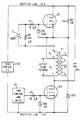
- the transformer T1 is comprised of a primary winding having a bootstrap section P, extending between terminaly 5 and 6 and a main primary winding section P 2 extending between terminals 4 and 5. Terminal 5 effectively taps the primary winding into two sections.
- the transformer T1 has a secondary winding S which is generally centertapped and connected to a rectifying load, which load is not shown for purposes of simplicity.
- An electronic switch Q1 connects one primary winding of the transformer, at terminal 5, to the source of rectified voltage appearing on the positive voltage line from the DC power supply source 50.
- Switch Q1 is an N-channel enhancement MOS device.
- the gate of switch Q1 is connected serially to the primary winding section P, via a resistance R1 and a capacitance C1, with a resistor R2 connected in parallel across capacitor C1.
- the gate of Q1 is connected to terminal 5 of the primary winding of transformer T1 by a Zener diode ZR1, which diode in the preferred embodiment has an avalanche voltage of 6.8 volts.
- a resistor R3 is connected across the source and drain terminals of the switch Q1.
- a second electronic switch Q2, which is also an MOS device, has its gate connected by means of a resistor R4 to the output of a pulse width modulation control and drive circuit 20.
- the gate of switch Q2 is also connected by means of a Zener diode ZR4 to the negative voltage line from the power supply source 50.
- the switch Q2 connects the terminal 4 of the primary winding to the negative voltage line when the gate voltage turns the switch Q2 on.
- a diode CR2 serves to clamp the primary transformer terminal 5 to the negative voltage line.
- a diode CR3 serves to clamp the transformer terminal 4 to the positive voltage line.
- the pulse width modulator control 20 turns Q2 on.
- Q 1 's output capacitance Coss is essentially discharged, placing nearly all of the supply voltage across the primary winding section P2 of transformer T1.
- the extra turns comprising the bootstrap winding appearing between terminals 5 and 6 of the primary are designed to develop approximately 12 to 14 volts, while C 1 is selected to be larger than the input capacitance C iss of Q1. Consequently, the input capacitance C iss is almost instantaneously charged to a voltage above Q1's threshold voltage, turning Q1 on.
- Zener diode ZR1 limits the gate voltage on Q1 to a safe value while the resistors R1 and R2 limit the amount of current that may flow through the Zener diode ZR1.
- the leakage inductance in transformer T1 will be adequate to delay the appearance of reflected loads in the primary until after switch Q1 has been turned on.
- the presence of the primary voltage keeps Q1 turned on until switch Q2 is switched off.
- switch Q2 is turned off.
- stored energy in transformer T1 causes a voltage reversal at terminals 4, 5 and 6.
- this voltage is clamped at 1 or 2 volts while core reset current flows through diode CR3 and switch Q1. This interval ends as soon as Q1's voltage V GS between the gate and source drops below the turn-on threshold voltage V TH .
- the stored charge on capacitor C1 contributes to fast reversal of the voltage V G s. After Q1 turns off, the induced voltage across transformer T1 rises to the supply voltage.
- Capacitors (not shown) associated with the supply voltage store the energy from transformer T1 received through the conduction of diodes CR2 and CR3.
- the rest period is approximately equal to the preceding «on» time of the converter.
- the transformer T1 induced voltage causes a reversed current to flow through Zener diode ZR1 and the combination of capacitor C 1 and resistor R2, thereby charging C1.
- the transformer T 1 induced voltage collapses to zero and the charge on capacitor C 1 transfers to the gate source capacitance C GS to effect switch Q1 turn-on. This turn-on occurs during the converter «off» time while switch Q2 is held off.
- This turn-on time is important in that it discharges Q1's output capacitance Coss and increases the effective value of Coss as V DS reduces, V DS being the voltage across the drain and source of Q1. These two conditions contribute to the subsequent turn-on of Q1 at the next converter on time.
- the function of resistor R3 is to keep Q1 Coss discharged after the charge on Q1 decays and allows Q1 to turn off.
- switches Q1 and Q2 are IRF 730 devices.
- the primary section P 2 transformer T has 60 turns and the bootstrap section P, has 4 turns.
- the nominal voltage from the power supply 50 appearing between the high and low rails is 336 volts D.C.
Landscapes
- Engineering & Computer Science (AREA)
- Power Engineering (AREA)
- Dc-Dc Converters (AREA)
Claims (3)
Applications Claiming Priority (2)
| Application Number | Priority Date | Filing Date | Title |
|---|---|---|---|
| US707289 | 1985-03-01 | ||
| US06/707,289 US4594649A (en) | 1985-03-01 | 1985-03-01 | Bootstrap drive for a two-transistor forward converter |
Publications (2)
| Publication Number | Publication Date |
|---|---|
| EP0216821A1 EP0216821A1 (de) | 1987-04-08 |
| EP0216821B1 true EP0216821B1 (de) | 1989-09-27 |
Family
ID=24841116
Family Applications (1)
| Application Number | Title | Priority Date | Filing Date |
|---|---|---|---|
| EP86901687A Expired EP0216821B1 (de) | 1985-03-01 | 1986-02-24 | Gleichstromwandler |
Country Status (5)
| Country | Link |
|---|---|
| US (1) | US4594649A (de) |
| EP (1) | EP0216821B1 (de) |
| JP (1) | JPS62502024A (de) |
| DE (1) | DE3665966D1 (de) |
| WO (1) | WO1986005333A1 (de) |
Families Citing this family (13)
| Publication number | Priority date | Publication date | Assignee | Title |
|---|---|---|---|---|
| US4757433A (en) * | 1987-01-07 | 1988-07-12 | Display Components, Inc. | Power supply |
| JP2711315B2 (ja) * | 1987-05-07 | 1998-02-10 | ニシム電子工業株式会社 | スイッチング電源装置 |
| US4835454A (en) * | 1987-12-15 | 1989-05-30 | Sundstrand Corp. | Advanced feed forward switch mode power suppply control |
| US4870553A (en) * | 1988-11-04 | 1989-09-26 | Compaq Computer Corporation | Double-switched flyback power-converter |
| US5677605A (en) * | 1989-08-22 | 1997-10-14 | Unique Mobility, Inc. | Brushless DC motor using phase timing advancement |
| US4974142A (en) * | 1990-02-20 | 1990-11-27 | Leslie Alexander D | Bootstrap drive for a switch-mode power converter |
| US5146396A (en) * | 1991-06-17 | 1992-09-08 | At&T Bell Laboratories | Single stage power factor corrected converter having isolated output |
| US5155670A (en) * | 1991-09-24 | 1992-10-13 | Brian Matley J | Bootstrap modified topologies for wide-input range switchmode DC to DC converters |
| FR2682543B1 (fr) * | 1991-10-09 | 1997-06-20 | Sgs Thomson Microelectronics | Circuit de commande de regulateur en demi-pont asymetrique. |
| US5666280A (en) * | 1993-05-07 | 1997-09-09 | Philips Electronics North America Corporation | High voltage integrated circuit driver for half-bridge circuit employing a jet to emulate a bootstrap diode |
| US5694303A (en) * | 1995-11-07 | 1997-12-02 | Interpoint Corporation | Semi-regulated power supply using forward converter leakage energy |
| AT504961B1 (de) * | 2006-12-19 | 2010-01-15 | Siemens Ag Oesterreich | Schaltungsanordnung zur reduzierten schalterbelastung |
| US11323035B2 (en) * | 2017-06-02 | 2022-05-03 | Drive Cjsc | DC voltage-pulse voltage converter |
Family Cites Families (5)
| Publication number | Priority date | Publication date | Assignee | Title |
|---|---|---|---|---|
| US3697852A (en) * | 1971-04-30 | 1972-10-10 | Ibm | Transistor switching regulator |
| US3742330A (en) * | 1971-09-07 | 1973-06-26 | Delta Electronic Control Corp | Current mode d c to a c converters |
| US3946301A (en) * | 1974-11-06 | 1976-03-23 | Computer Power, Inc. | Direct current to alternating current electronic inverter with overload and short-circuit protection circuitry |
| US4318168A (en) * | 1980-06-27 | 1982-03-02 | Raytheon Company | Over stress sense circuit for flyback power supply |
| US4479175A (en) * | 1982-08-13 | 1984-10-23 | Honeywell Inc. | Phase modulated switchmode power amplifier and waveform generator |
-
1985
- 1985-03-01 US US06/707,289 patent/US4594649A/en not_active Expired - Lifetime
-
1986
- 1986-02-24 EP EP86901687A patent/EP0216821B1/de not_active Expired
- 1986-02-24 DE DE8686901687T patent/DE3665966D1/de not_active Expired
- 1986-02-24 WO PCT/US1986/000381 patent/WO1986005333A1/en not_active Ceased
- 1986-02-24 JP JP61501482A patent/JPS62502024A/ja active Pending
Also Published As
| Publication number | Publication date |
|---|---|
| DE3665966D1 (en) | 1989-11-02 |
| JPS62502024A (ja) | 1987-08-06 |
| US4594649A (en) | 1986-06-10 |
| EP0216821A1 (de) | 1987-04-08 |
| WO1986005333A1 (en) | 1986-09-12 |
Similar Documents
| Publication | Publication Date | Title |
|---|---|---|
| US5590032A (en) | Self-synchronized drive circuit for a synchronous rectifier in a clamped-mode power converter | |
| US5726869A (en) | Synchronous rectifier type DC-to-DC converter in which a saturable inductive device is connected in series with a secondary-side switching device | |
| US6643144B2 (en) | Circuit configuration for applying a supply voltage to a load and method for such application | |
| US4511815A (en) | Transformer-isolated power MOSFET driver circuit | |
| EP0913026B1 (de) | Eintakt-durchflussumrichter für gleichstrom-gleichstrom-umwandlung mit verbesserter rücksetzung für synchrongleichrichtung | |
| US4172277A (en) | Chopping control system for a converter in a DC electrical power supply | |
| US4754385A (en) | Two transistor flyback switching converter with current sensing for discontinuous operation | |
| US10516341B1 (en) | Synchronous rectifier gate voltage boost method and system | |
| US10523110B2 (en) | Synchronous rectifier controller for offline power converter and method therefor | |
| EP0216821B1 (de) | Gleichstromwandler | |
| US5694303A (en) | Semi-regulated power supply using forward converter leakage energy | |
| JP2004015886A (ja) | 同期整流の駆動回路 | |
| US4464585A (en) | Gate circuit of gate turn-off thyristor | |
| US5103386A (en) | Flyback converter with energy feedback circuit and demagnetization circuit | |
| US6791849B2 (en) | Synchronous rectifying circuit for flyback converter | |
| US4308577A (en) | Base drive circuit | |
| US20060018133A1 (en) | Switching mode power converter having secondary side bias generating and driving circuit to provide synchronous rectification and active clamp | |
| KR20030011293A (ko) | 비최적 리셋 2차 전압을 위한 자체 구동 동기 정류기회로 | |
| US20020021578A1 (en) | Synchronous rectification circuit of DC-DC converter | |
| US6370051B1 (en) | Forward converter circuit having reduced switching losses | |
| US4694207A (en) | FET gating circuit for switching electrical loads | |
| US4899065A (en) | Pre-drive circuit | |
| US4974142A (en) | Bootstrap drive for a switch-mode power converter | |
| US4323957A (en) | Voltage supression circuit for a voltage converter circuit | |
| JPH0636392U (ja) | フライバック型コンバータ |
Legal Events
| Date | Code | Title | Description |
|---|---|---|---|
| PUAI | Public reference made under article 153(3) epc to a published international application that has entered the european phase |
Free format text: ORIGINAL CODE: 0009012 |
|
| AK | Designated contracting states |
Kind code of ref document: A1 Designated state(s): DE FR GB |
|
| 17P | Request for examination filed |
Effective date: 19870226 |
|
| DET | De: translation of patent claims | ||
| 17Q | First examination report despatched |
Effective date: 19880808 |
|
| GRAA | (expected) grant |
Free format text: ORIGINAL CODE: 0009210 |
|
| AK | Designated contracting states |
Kind code of ref document: B1 Designated state(s): DE FR GB |
|
| REF | Corresponds to: |
Ref document number: 3665966 Country of ref document: DE Date of ref document: 19891102 |
|
| ET | Fr: translation filed | ||
| PLBE | No opposition filed within time limit |
Free format text: ORIGINAL CODE: 0009261 |
|
| STAA | Information on the status of an ep patent application or granted ep patent |
Free format text: STATUS: NO OPPOSITION FILED WITHIN TIME LIMIT |
|
| 26N | No opposition filed | ||
| PGFP | Annual fee paid to national office [announced via postgrant information from national office to epo] |
Ref country code: GB Payment date: 19911231 Year of fee payment: 7 |
|
| PGFP | Annual fee paid to national office [announced via postgrant information from national office to epo] |
Ref country code: FR Payment date: 19920130 Year of fee payment: 7 |
|
| PGFP | Annual fee paid to national office [announced via postgrant information from national office to epo] |
Ref country code: DE Payment date: 19920325 Year of fee payment: 7 |
|
| PG25 | Lapsed in a contracting state [announced via postgrant information from national office to epo] |
Ref country code: GB Effective date: 19930224 |
|
| REG | Reference to a national code |
Ref country code: FR Ref legal event code: TP |
|
| GBPC | Gb: european patent ceased through non-payment of renewal fee |
Effective date: 19930224 |
|
| PG25 | Lapsed in a contracting state [announced via postgrant information from national office to epo] |
Ref country code: FR Effective date: 19931029 |
|
| PG25 | Lapsed in a contracting state [announced via postgrant information from national office to epo] |
Ref country code: DE Effective date: 19931103 |
|
| REG | Reference to a national code |
Ref country code: FR Ref legal event code: ST |