EP0217427A1 - Schaltnetzteil mit einem Leistungsschalter - Google Patents
Schaltnetzteil mit einem Leistungsschalter Download PDFInfo
- Publication number
- EP0217427A1 EP0217427A1 EP86201373A EP86201373A EP0217427A1 EP 0217427 A1 EP0217427 A1 EP 0217427A1 EP 86201373 A EP86201373 A EP 86201373A EP 86201373 A EP86201373 A EP 86201373A EP 0217427 A1 EP0217427 A1 EP 0217427A1
- Authority
- EP
- European Patent Office
- Prior art keywords
- switch
- voltage
- transistor
- instant
- power supply
- Prior art date
- Legal status (The legal status is an assumption and is not a legal conclusion. Google has not performed a legal analysis and makes no representation as to the accuracy of the status listed.)
- Granted
Links
- 238000004804 winding Methods 0.000 claims abstract description 71
- 230000007423 decrease Effects 0.000 claims abstract description 16
- 230000010355 oscillation Effects 0.000 claims description 12
- 230000000977 initiatory effect Effects 0.000 claims description 9
- 238000009877 rendering Methods 0.000 claims description 4
- 239000003990 capacitor Substances 0.000 description 62
- 230000002441 reversible effect Effects 0.000 description 7
- 230000003071 parasitic effect Effects 0.000 description 4
- 239000002800 charge carrier Substances 0.000 description 3
- 230000009467 reduction Effects 0.000 description 3
- 230000003111 delayed effect Effects 0.000 description 2
- 230000002349 favourable effect Effects 0.000 description 2
- 238000009499 grossing Methods 0.000 description 2
- 238000000034 method Methods 0.000 description 2
- 230000008569 process Effects 0.000 description 2
- 230000008901 benefit Effects 0.000 description 1
- 230000003247 decreasing effect Effects 0.000 description 1
- 230000002950 deficient Effects 0.000 description 1
- 230000001419 dependent effect Effects 0.000 description 1
- 238000010586 diagram Methods 0.000 description 1
- 230000006872 improvement Effects 0.000 description 1
- 230000010354 integration Effects 0.000 description 1
- 230000005855 radiation Effects 0.000 description 1
- 229920006395 saturated elastomer Polymers 0.000 description 1
- 230000009466 transformation Effects 0.000 description 1
Images

Classifications
-
- H—ELECTRICITY
- H02—GENERATION; CONVERSION OR DISTRIBUTION OF ELECTRIC POWER
- H02M—APPARATUS FOR CONVERSION BETWEEN AC AND AC, BETWEEN AC AND DC, OR BETWEEN DC AND DC, AND FOR USE WITH MAINS OR SIMILAR POWER SUPPLY SYSTEMS; CONVERSION OF DC OR AC INPUT POWER INTO SURGE OUTPUT POWER; CONTROL OR REGULATION THEREOF
- H02M3/00—Conversion of DC power input into DC power output
- H02M3/22—Conversion of DC power input into DC power output with intermediate conversion into AC
- H02M3/24—Conversion of DC power input into DC power output with intermediate conversion into AC by static converters
- H02M3/28—Conversion of DC power input into DC power output with intermediate conversion into AC by static converters using discharge tubes with control electrode or semiconductor devices with control electrode to produce the intermediate AC
- H02M3/325—Conversion of DC power input into DC power output with intermediate conversion into AC by static converters using discharge tubes with control electrode or semiconductor devices with control electrode to produce the intermediate AC using devices of a triode or a transistor type requiring continuous application of a control signal
- H02M3/335—Conversion of DC power input into DC power output with intermediate conversion into AC by static converters using discharge tubes with control electrode or semiconductor devices with control electrode to produce the intermediate AC using devices of a triode or a transistor type requiring continuous application of a control signal using semiconductor devices only
- H02M3/338—Conversion of DC power input into DC power output with intermediate conversion into AC by static converters using discharge tubes with control electrode or semiconductor devices with control electrode to produce the intermediate AC using devices of a triode or a transistor type requiring continuous application of a control signal using semiconductor devices only in a self-oscillating arrangement
-
- H—ELECTRICITY
- H02—GENERATION; CONVERSION OR DISTRIBUTION OF ELECTRIC POWER
- H02M—APPARATUS FOR CONVERSION BETWEEN AC AND AC, BETWEEN AC AND DC, OR BETWEEN DC AND DC, AND FOR USE WITH MAINS OR SIMILAR POWER SUPPLY SYSTEMS; CONVERSION OF DC OR AC INPUT POWER INTO SURGE OUTPUT POWER; CONTROL OR REGULATION THEREOF
- H02M3/00—Conversion of DC power input into DC power output
- H02M3/22—Conversion of DC power input into DC power output with intermediate conversion into AC
- H02M3/24—Conversion of DC power input into DC power output with intermediate conversion into AC by static converters
- H02M3/28—Conversion of DC power input into DC power output with intermediate conversion into AC by static converters using discharge tubes with control electrode or semiconductor devices with control electrode to produce the intermediate AC
- H02M3/325—Conversion of DC power input into DC power output with intermediate conversion into AC by static converters using discharge tubes with control electrode or semiconductor devices with control electrode to produce the intermediate AC using devices of a triode or a transistor type requiring continuous application of a control signal
- H02M3/335—Conversion of DC power input into DC power output with intermediate conversion into AC by static converters using discharge tubes with control electrode or semiconductor devices with control electrode to produce the intermediate AC using devices of a triode or a transistor type requiring continuous application of a control signal using semiconductor devices only
- H02M3/338—Conversion of DC power input into DC power output with intermediate conversion into AC by static converters using discharge tubes with control electrode or semiconductor devices with control electrode to produce the intermediate AC using devices of a triode or a transistor type requiring continuous application of a control signal using semiconductor devices only in a self-oscillating arrangement
- H02M3/3385—Conversion of DC power input into DC power output with intermediate conversion into AC by static converters using discharge tubes with control electrode or semiconductor devices with control electrode to produce the intermediate AC using devices of a triode or a transistor type requiring continuous application of a control signal using semiconductor devices only in a self-oscillating arrangement with automatic control of output voltage or current
-
- Y—GENERAL TAGGING OF NEW TECHNOLOGICAL DEVELOPMENTS; GENERAL TAGGING OF CROSS-SECTIONAL TECHNOLOGIES SPANNING OVER SEVERAL SECTIONS OF THE IPC; TECHNICAL SUBJECTS COVERED BY FORMER USPC CROSS-REFERENCE ART COLLECTIONS [XRACs] AND DIGESTS
- Y02—TECHNOLOGIES OR APPLICATIONS FOR MITIGATION OR ADAPTATION AGAINST CLIMATE CHANGE
- Y02B—CLIMATE CHANGE MITIGATION TECHNOLOGIES RELATED TO BUILDINGS, e.g. HOUSING, HOUSE APPLIANCES OR RELATED END-USER APPLICATIONS
- Y02B70/00—Technologies for an efficient end-user side electric power management and consumption
- Y02B70/10—Technologies improving the efficiency by using switched-mode power supplies [SMPS], i.e. efficient power electronics conversion e.g. power factor correction or reduction of losses in power supplies or efficient standby modes
Definitions
- the invention relates to a switched-mode power supply circuit for converting a d.c. input voltage into a d.c. output voltage, including a controllable power switch arranged in series with the primary winding of a transformer, the series arrangement thus formed being coupled to the input voltage terminals, said transformer having a secondary winding to which a rectifier is coupled for providing the output voltage, the primary winding forming part of a resonant circuit when switch and rectifier pass no current, a drive circuit including a delay network being connected to a control electrode of the switch for each time initiating turning off of the switch, whereafter the voltage across the switch increases to a given value and substantially maintains said value, whereafter the said voltage decreases in accordance with an oscillation with the resonance frequency, and for each time initiating turning on of the switch, whereafter the voltage across the switch is substantially zero.
- a power supply circuit of this type is known from United States Patent Specification 4,183,080. It is a self-oscillating circuit in which the drive circuit for the power switch, which is a switching transistor, includes a secondary winding of the transformer, which secondary winding is coupled with the primary winding with a positive feedback. A network for rendering the transistor conductive and for maintaining this state is incorporated between the said secondary winding and the base of the transistor.
- the drive circuit includes a delay network connected to the same winding and a drive transistor whose main path is arranged in parallel with the base emitter diode of the switching transistor.
- the drive transistor becomes conducting so that the switching transistor is rapidly rendered non- conducting In this manner the turn-off losses of this transistor are reduced, more specifically because of the short duration of the turn-off process.
- the conducting time of the drive transistor is very short. Together with parasitic capacitances the primary winding constitutes a resonant circuit.
- the invention is based on the recognition that means can be used in such a power supply circuit which are similar to those used in the said known circuit for reducing the turn-on losses of the power switch.
- the power supply circuit according to the invention is characterized in that the delay network is coupled to the control electrode of the power switch for each time adjusting the turning on of said switch at an instant which is substantially half a cycle of the resonance frequency later than the initial instant of the decrease of the voltage across the switch during its previous cut-off time.
- a power supply circuit in which the delay network is coupled to the control electrode of a second switch which is conducting at the end of the conducting period of the power switch for initiating the turn-off of said power switch may advantageously be characterized by means for each time rendering the second switch conducting substantially at the initial instant of the decrease of the voltage across the power switch and for subsequently maintaining the second switch in the conducting state during substantially half a cycle of the resonance frequency after the said instant. In this manner the second switch has a second function, which is cost-saving.
- a power supply circuit in which the delay network is connected to a further secondary winding of the transformer is characterized in that, during operation, the voltage at the junction of the delay network and the said further secondary winding has the same polarity as the voltage at the junction of the primary winding and the power switch.
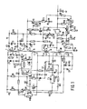
- the self-oscillating power supply circuit of Figure 1 comprises an npn power switching transistor Tr1 whose collector is connected to the primary winding L1 of a transformer T, while the emitter is connected to ground.
- the other end of winding L1 is connected to the positive rail of an unstabilized voltage supply source V B whose negative rail is also connected to ground and which is, for example, a mains rectifier.
- the turn-on path of transistor Tr1, 4tch is connected to the base of the transistor and the other end of which is connected to ground, comprises a capacitor C1, a feedback winding L2 of transformer T, a diode D1 and a resistor R1.
- the base current flowing during the conducting period of transistor Tr1 produces a negative voltage across capacitor C1.
- the turn-off path of transistor Tr1 which is likewise connected to the base thereof, comprises capacitor C1, the emiter-collector path of a pnp transistor Tr2 having a base-emitter resistor R2, and an inductance L3.
- a reverse base current of transistor Tr1 flows through elements L1, Tr2 and L3 so that the charge carriers stored in this transistor during the conducting period are removed.
- a further winding L4 of transformer T and a diode D2 a negative voltage for capacitor C1 is generated in case the forward base current of transistor Tr1 flows too short a time under given circumstances to built up a sufficiently constant voltage across capacitor C1.
- the winding sense of the windings of transformer T is indicated by means of dots.
- Winding L5 has such a winding sense and diode D3 has such a conductivity direction that a charge current for capacitor C2 flows through resistor R3 during the conducting period of transistor Tr1.
- the other end of capacitor C2 is connected to the junction of capacitor C1, winding L2 and the collector of transisbor Tr2. With respect to the d.c. voltage level present at this junction a sawtooth voltage is produced across capacitor C2 which voltage is passed on via an RC parallel network R4, C3 to the base of an npn transistor Tr4.
- transistor Tr4 The emitter of transistor Tr4 is connected to the said junction, while the collector is connected to the base of transistor Tr2. At a given instant the voltage at the base of transistor Tr4reaches a value at which the transistor is rendered conducting. As a result transistor Tr2 is also rendered conducting. The voltage at the emitter of this transistor assumes substantially the same value as the negative voltage of approximately -5 V which is present across capacitor C1, which initiates the turn-off of transistor Tr1. During the period of time when transistor Tr1 is non-conductive capacitor C2 is discharged via a resistor R5, a diode D4 and winding L4 while a reverse current flows through transistor Tr2 which current also flows through resistor R1 and through a capacitor C4 which is arranged in parallel with diode D1.
- a starting resistor R6 having a high value is arranged between the positive rail of source V B and the base of transistor Tr2.
- a current flows through resistors R 6 and R2 which also flows through capacitor C4 and winding L2 so that energy is built up in transformer T. Due to this current the voltage at the base of transistor Tr1 increases until the value is reached at which the transistor becomes conducting. Also during normal operation a current flows through resistor R6, but its value is too'low to have a noticeable influence on the behaviour of the circuit.
- FIG. 1 shows a number of these windings, for example, L6 and L7.
- transistor Tr1 When transistor Tr1 is turned off, a current recharging smoothing capacitors C5 and C6 through rectifiers, for example, D5 and D6, respectively, flows through each secondary winding.
- the other ends of capacitors C5 and C6 are connected to ground.
- the voltages across these capacitors are the output voltages of the supply circuit for loads connectable thereto.
- These loads which are not shown in Figure 1, are, for example, parts of a television receiver.
- a network with a tuning capacitor C7 and a dampingresistor R7, as well as a clamping network with a diode D7 is arranged in parallel with winding L1.
- Winding L1 and capacitor C7, as well as parasitic capacitances, constitute a resonant circuit in which an oscillation is produced in the intervals when no current flows through transistor Tr1 and rectifiers D5 and D6.
- the circuit includes a light-emitting diode D8 which is optically coupled to a light-sensitive npn transistor Tr5 an emitter resistor R8 of which is connected in the base load of transistor Tr4 with the network R4, C3 and a collector resistor R9 of which is connected to source V Bt while the base is unconnected.
- the collector of transistor Tr5 is also connected at one end via an RC parallel network R10, C8 to the junction of windings L2 and L4 and capacitor C1 and at the other end via a diode D9 to the junction of winding L2 and diode D1.
- a positive voltage is thus present at the said collector. If the current through diode D8 varies in a manner to be explained hereinafter, the emitter current of transistor Tr5 also varies. An increase thereof, for example, involves an increase in the voltage at the base of transistor Tr3 so that transistor Tr1 isturned off at an earlier instant than would otherwise be the case. The final value of transistor Tr1 is thus lower, resulting in the output voltages of the circuit also being lower.
- a network including a Zener diode D10 which is connected between the junction of resistors R4 and R8 and the junction of resistor R3 and diode D3, this control is also dependent on variations of the voltage V B .
- Figure 2 shows some idealized waveforms: Figure 2a shows the variation as a function of time of the voltage v across winding L1, i.e. the same variation but for a d.c. level, more specifically that of source V B , as that of the voltage at the collector of transistor Tr1, and Figure 2b shows the variation of the current i flowing through winding L1.
- Transistor Tr1 is turned off at an instant t . 0 Before this instant current i increases linearly, while voltage v has the value -V B . After instant to voltage v increases in accordance with a sine function of time, whereas current i varies in accordance with a consine function. At an instant t 1 voltage v reaches the zero value and current i is at a maximum. Voltage v continues to increase until the value is reached at an instant t 2 when the rectifiers on the secondary side start conducting.
- FIGS. 1 and 2a show that transistor Tr1 would thereby be rendered conducting at an instant after instant t 3 when the sum of the voltage across winding L2 and the voltage across capacitors Cl and C4 will be lower than the base-emitter threshold voltage of the transistor. This instant occurs shortly after instant t 3 before voltage v becomes zero, i.e. upon turning on, the voltage at the collector of transistor Tr1 would be slightly lower than the value V B + nV o .
- transistor Tr1 The turn-off losses of transistor Tr1 are reduced in known manner by incorporating inductance L3 in the base lead.
- the superfluous charge carriers of the transistor are thereby slowly removed, while the collector current continues to flow, more specifically until the moment when the transistor comes out of its saturated state resulting in a very rapid decrease to zero of the collector current.
- the voltage at the collector of transistor Tr1 is fairly high upon turning on which causes a considerable switching dissipation in transistor Tr1 and in resistor R7.
- the circuit of Figure 1 includes an npn transistor Tr3 whose emitter is connected to the junction of capacitor C1 and winding L2 and whose collector is connected to the base of transistor Tr2 via a diode D11 which has the same conductivity direction as the collector-emitter path of transistor Tr3.
- a winding L8 of transformer T isconnected at one end to the emitter of transistor Tr3 and at the other end to an integrating network consisting of a resistor R11 and a capacitor C9, said capacitor being arranged between resistor R9 and the said emitter.
- the junction of capacitor C9 and resistor R11 is connected via a limiting resistor R12 to the base of transistor Tr3.
- winding sense of winding L8 is such that the voltage at the junction of resistor R11 has the same polarity as the voltage indicated in Figure 2a, i.e. the voltage under consideration is negative before instant t 1 and positive after this instant.
- the voltage v' across capacitor C9 which is proportional to the integral of the voltage at the last-mentioned junction has the same time variation as current i in Figure 2a but a polarity which is opposed thereto.
- current i is proportional to the integral of voltage v.
- Figure 2c shows the variation of voltage v'. Since both the voltage across winding L8 and the current through capacitor C9 have a mean value of zero over one oscillation period, the mean value of voltage v' is also zero. This means that voltage v' reverses its polarity and becomes positive at an instant t 6 which is located earlier than instant t 3 .
- the time constant of the RC network R11, C9 is chosen to be such that voltage v' exceeds the value of the base-emitter threshold voltage of transistor Tr3 after instant t 3 . This shows that this transistor conducts after instant t 3 and maintains transistor Tr1 in the non-conducting state in the same manner as transistor Tr4 does at instant t , more speci- fically because transistor Tr2 conducts.
- the circuit may be dimensioned in such a manner that this interval substantially coincides with the period between instants t 3 and t S .
- the resistors R11 and R12 had values of approximately 8.2 and 2.2 k ⁇ , respectively, while the capacitance of capacitor C9 was approximately 4.7 nF, with the frequency of the oscillation, i.e. the inverse of the period between instants to and t 7 , could vary between 25 and 60kHz.
- the turn-on instant of transistor Tr1 cannot be adjusted at instant t 5 by means of a d.c. voltage level in the base lead of the transistor so that at first sight a delay could be obtained.
- a diode may be arranged in series with the transistor and with the same conductivity direction as this transistor, while the anti-parallel diode is arranged between the junction of the series diode with winding L1 and ground.
- the dissipation caused by the reverse current is smaller in this case because the voltage at the collector is maintained at a low value by the conducting anti-parallel diode than the dissipation caused by the forward current in Figure 2 which is many times larger, namely proportional to lcv2 and to the oscillation frequency.
- C is the capacitance which is effectively in parallel with transistor Tr1.
- the said reverse current returns to source Y B .
- the series arrangement of a diode D14 and a capacitor C10 is connected to a secondary winding L9 of transformer T, the anode of diode D14 being connected to the end of winding L9 which is not connected to ground.
- One end of a further secondary winding L10 of transformer T which has more turns than winding L9 is connected to the junction of diode D14 and capacitor C10 and the other end is connected to the cathode of a thyristor Th.
- the anode of thyristor Th is connected to ground.
- a series arrangement constituted by the emitter-collector path of a pnp transistor Tr6, a diode D15 and a voltage divider consisting of two resistors R13 and R14 is arranged in parallel with capacitor C10.
- the emitter of transistor Tr6 is connected to the input of a series control circuit S the output voltage of which is smoothed by means of a capacitor C11.
- the series arrangement of the emitter-collector path of a pnp transistor Tr7, a resistor R15 and the above-mentioned light-emitting diode D8 is arranged in parallel with capacitor C11.
- the base of an npn transistor Tr8 is connected to the junction of resistors R13 and R14, while the collector is connected to the base of transistor Tr7 and to a resistor R16 and the emitter is connected to the cathode of a Zener diode D16 the other end of which is connected to ground.
- the other end of resistor R16 is connected to the output of circuit S.
- a diode D17 is incorporated between the collector of transistor Tr6 and the cathode gate of thyristor Th having the same conductivity direction as transistor Tr6 and an RC series network R17, C12 is incorporated between the base of transistor Tr8 and the collector of transistor Tr7. Finally a resistor R18 connects the base of transistor Tr6 with a terminal A.
- transistor Tr6 In the normal operating state transistor Tr6 is not conducting because terminal A is either not connected or is connected to a positive voltage. Diode D17 neither conducts and therefore thyristor Th does not either. Consequently winding L10 remains currentless and capacitor C10 carries a d.c. voltage of, for example, approximately 7 V which is derived by means of diode D14 from the voltage across winding L9. A voltage of, for example, 5 V for a microprocessor in the control section of the receiver and for remote control is present across capacitor C11. Transistors Tr7 amd Tr8 also remain non-conducting.
- the supply circuit is provided with a further secondary winding L11 of transformer T, a rectifier D18 and a smoothing capacitor C13 for controlling the output voltages of this circuit.
- a voltage divider arranged in parallel with capacitor C5 and consisting of resistors R19, R20, R21 and R22, the base of an npn transistor Tr9, which is connected to the junction of resistors R20 and R21, is adjusted to a d.c. voltage which is proportional to the output voltage V across capacitor C5.
- the emitter of transistor Tr9 is connected to Zener diode D16.
- transistor Tr9 the voltage at the base is compared with the voltage of diode D16.
- the difference measured determines the collector current of a pnp transistor Tr10 whose emitter is connected to capacitor C13 and whose collector is connected via a resistor R23 to the anode of diode D8 and consequently determines the current through diode D8 and therefore the emitter current of transistor Tr5. If, for example, the output voltage increases as a result of a decreasing load and/or as a result of an increase of voltage V B , the collector current of transistor Tr9 and hence the control current through diode D8 also increase. In the manner already explained this increase causes a reduction in the conductivity period of transistor Tr1, which counteracts the increase of the output voltage.
- An RC series network R24, C14 is incorporated between the base and the collector of transistor Tr10 for the purpose of reducing the loop gain at a high frequency and thus for improving the stability of the control.
- a diode D19 which is arranged between capacitor C6 and the junction of resistors R19 and R20 ensures a safeguard if diode D5 with which the highest output voltage V is generated becomes defective. In this case, in which diode D5 is interrupted, the voltage across capacitor C5 becomes zero. The control then attempts to increase this voltage: this is prevented because D19 starts conducting so that now the voltage across capacitor C6 is controlled.
- transistors Tr7 and Tr8 constitute a monostable multivibrator which remains in its state reached during a period which is determined, inter alia, by the time constant of network R17, C12 even after the voltage V 1 across capacitor C10 has become low.
- transistor Tr8 a part of voltage V 1 is compared with the voltage of Zener diode D16. The difference measured determines the collector current of transistor Tr7, which current flows through diode D8.
- the part of the circuit with winding L10 thus forms part of a control loop for maintaining voltage V substantially constant, which control loop is put into operation by switching over to the stand-by state by means of terminal A.
- the number of turns of winding L10 has been chosen to be such that during the stand-by state the output voltages of the supply circuit, i.e. the direct voltages derived from the other secondary windings L6, L7 and L11 are reduced to low values with little power being dissipated in the loads. This may be explained with reference to the following figures.
- winding L6 has 44 turns
- L7 has 7 turns
- L9 has 2 turns
- L10 has 15 turns, respectively
- the voltage across capacitor C10 is :
- the conduction period of transistor Tr1 i.e. the interval between instants t 5 and t 7 in Figure 1
- This conduction period has, however, a minimum value which is determined by the storage period of the charge carriers in transistor Tr1.
- the collector current of this transistor increases to a peak value which depends on the said period and also on voltage V B and which, likewise as the storage period, is subject to variations caused by tolerances. Due to this current more energy is stored in transformer T than is extracted from it so that the output voltages tend to increase again after having been low.
- diode D8 causes such a high control current that transistor Tr1 is turned off and remains non-conducting because transistor Tr4 continuously remains conducting due to the large emitter current of transistor Tr5.
- transistor Tr5 has a collector voltage via resistor R9.
- the output voltages and also the control current then decrease again because capacitors C5, C6, C10 and C13 are discharged, more specifically until voltage V 1 reaches a value at which the power supply circuit starts again.
- Transistor Tr1 becomes conducting in the manner already described, resulting in the capacitors on the secondary side of transformer T being charged again.
- An intermitting current flows through thyristor Th so that the voltage across capacitor C10 reaches a level at which transistor Tr8 is rendered conducting again, which restores the control loop. The process described is subsequently repeated.
- transistor Tr1 which may be replaced by an equivalent power switch, for example, a gate turn-off switch.
- transistor Tr1 which may be replaced by an equivalent power switch, for example, a gate turn-off switch.
- circuit-technical details for example, the circuits for turning off transistor Tr1 or for turning on this transistor.
- transistor Tr1 at the desired instant winding L8 has been used in the foregoing, through which winding a current flows which has a simdar variation as the current i through winding L1.
- Figure 3 very diagrammatically shows such a circuit in which only the same elements Tr1, L1, L6, D5, C5 and C7 as in Figure 1 have been shown.
- a squarewave drive voltage is applied to the base of transistor Tr1 with the aid of an astable multivibrator M in Figure 3.
- multivibrator Mrece ives two trigger pulses P1 and P2, with the leading edge of pulse P1, whose time position is determined by a control circuit, initiating the turn-off of transistor Tr1 and with the laading edge of pulse P2 initiating the turn-on. Since the same waveforms as in Figure 2 under the same circumstances as in Figure 1 also apply to the circuit of Figure 3, pulse P2 can be generated by the same means as in Figure 1 for rendering a switch having the same function as transistor Tr3 in Figure 1 conducting for a short time.
- a variant of this measure which may also be used in the circuit of Figure 1, is the use of a level detector for determining the instant when the voltage at the collector of transistor Tr1 upon a decrease thereof after instant t 3 substantially reaches the value V B - nV and for delaying the turn-on until this instant.
- the leading edge of pulse P2 may be generated at the instant when the waveform of Figure 2c comes below a predetermined level.
Landscapes
- Engineering & Computer Science (AREA)
- Power Engineering (AREA)
- Dc-Dc Converters (AREA)
Applications Claiming Priority (2)
| Application Number | Priority Date | Filing Date | Title |
|---|---|---|---|
| NL8502339A NL8502339A (nl) | 1985-08-26 | 1985-08-26 | Geschakelde voedingsspanningsschakeling met een vermogensschakelaar. |
| NL8502339 | 1985-08-26 |
Publications (2)
| Publication Number | Publication Date |
|---|---|
| EP0217427A1 true EP0217427A1 (de) | 1987-04-08 |
| EP0217427B1 EP0217427B1 (de) | 1990-11-22 |
Family
ID=19846467
Family Applications (1)
| Application Number | Title | Priority Date | Filing Date |
|---|---|---|---|
| EP86201373A Expired - Lifetime EP0217427B1 (de) | 1985-08-26 | 1986-08-04 | Schaltnetzteil mit einem Leistungsschalter |
Country Status (8)
| Country | Link |
|---|---|
| US (1) | US4694385A (de) |
| EP (1) | EP0217427B1 (de) |
| JP (1) | JPS6248264A (de) |
| KR (1) | KR870002687A (de) |
| CN (1) | CN1011171B (de) |
| DE (1) | DE3675728D1 (de) |
| ES (1) | ES2001566A6 (de) |
| NL (1) | NL8502339A (de) |
Cited By (1)
| Publication number | Priority date | Publication date | Assignee | Title |
|---|---|---|---|---|
| EP0349080A1 (de) * | 1988-06-30 | 1990-01-03 | Koninklijke Philips Electronics N.V. | Geschaltete Speisespannungsschaltung |
Families Citing this family (7)
| Publication number | Priority date | Publication date | Assignee | Title |
|---|---|---|---|---|
| US4945465A (en) * | 1988-09-15 | 1990-07-31 | U.S. Philips Corporation | Switched-mode power supply circuit |
| NL8900509A (nl) * | 1989-03-02 | 1990-10-01 | Philips Nv | Geschakelde voedingsspanningsschakeling. |
| US4937727A (en) * | 1989-03-07 | 1990-06-26 | Rca Licensing Corporation | Switch-mode power supply with transformer-coupled feedback |
| DE19518863A1 (de) * | 1995-05-23 | 1996-11-28 | Thomson Brandt Gmbh | Schaltnetzteil mit Bereitschaftsbetrieb |
| JP3216598B2 (ja) * | 1998-02-09 | 2001-10-09 | 株式会社村田製作所 | スイッチング電源装置 |
| JP3351400B2 (ja) * | 1999-01-18 | 2002-11-25 | 株式会社村田製作所 | スイッチング電源装置 |
| JP3475904B2 (ja) | 2000-04-17 | 2003-12-10 | 株式会社村田製作所 | スイッチング電源装置 |
Citations (3)
| Publication number | Priority date | Publication date | Assignee | Title |
|---|---|---|---|---|
| US3846690A (en) * | 1972-07-11 | 1974-11-05 | Co Generale D Electricite | Device for charging an electric power storage element to a predetermined voltage |
| GB2018529A (en) * | 1978-04-06 | 1979-10-17 | Westfaelische Metall Industrie | DC-to-DC converters |
| WO1984004431A1 (en) * | 1983-04-25 | 1984-11-08 | Ncr Co | Voltage converter |
Family Cites Families (5)
| Publication number | Priority date | Publication date | Assignee | Title |
|---|---|---|---|---|
| NL7803661A (nl) * | 1978-04-06 | 1979-10-09 | Philips Nv | Afgestemde geschakelde voedingsspanningsschakeling. |
| US4183080A (en) * | 1978-06-21 | 1980-01-08 | Theodore Liebman | DC to DC converter |
| US4438485A (en) * | 1981-12-21 | 1984-03-20 | Voigt William C | Efficiency switching-mode power supply |
| NL8200616A (nl) * | 1982-02-17 | 1983-09-16 | Philips Nv | Geschakelde zelfoscillerende voedingsspanningsschakeling. |
| US4488210A (en) * | 1982-04-07 | 1984-12-11 | Sanyo Electric Co., Ltd. | Power supply circuit of switching regulator type |
-
1985
- 1985-08-26 NL NL8502339A patent/NL8502339A/nl unknown
-
1986
- 1986-07-30 US US06/890,593 patent/US4694385A/en not_active Expired - Fee Related
- 1986-08-04 EP EP86201373A patent/EP0217427B1/de not_active Expired - Lifetime
- 1986-08-04 DE DE8686201373T patent/DE3675728D1/de not_active Expired - Lifetime
- 1986-08-22 ES ES8601292A patent/ES2001566A6/es not_active Expired
- 1986-08-25 JP JP61197445A patent/JPS6248264A/ja active Pending
- 1986-08-25 KR KR1019860007013A patent/KR870002687A/ko not_active Abandoned
- 1986-08-26 CN CN86105460A patent/CN1011171B/zh not_active Expired
Patent Citations (3)
| Publication number | Priority date | Publication date | Assignee | Title |
|---|---|---|---|---|
| US3846690A (en) * | 1972-07-11 | 1974-11-05 | Co Generale D Electricite | Device for charging an electric power storage element to a predetermined voltage |
| GB2018529A (en) * | 1978-04-06 | 1979-10-17 | Westfaelische Metall Industrie | DC-to-DC converters |
| WO1984004431A1 (en) * | 1983-04-25 | 1984-11-08 | Ncr Co | Voltage converter |
Cited By (2)
| Publication number | Priority date | Publication date | Assignee | Title |
|---|---|---|---|---|
| EP0349080A1 (de) * | 1988-06-30 | 1990-01-03 | Koninklijke Philips Electronics N.V. | Geschaltete Speisespannungsschaltung |
| US4926304A (en) * | 1988-06-30 | 1990-05-15 | U.S. Philips Corporation | Switched-mode power supply with low loss interrupted oscillation |
Also Published As
| Publication number | Publication date |
|---|---|
| CN86105460A (zh) | 1987-02-25 |
| EP0217427B1 (de) | 1990-11-22 |
| NL8502339A (nl) | 1987-03-16 |
| DE3675728D1 (de) | 1991-01-03 |
| ES2001566A6 (es) | 1988-06-01 |
| JPS6248264A (ja) | 1987-03-02 |
| CN1011171B (zh) | 1991-01-09 |
| KR870002687A (ko) | 1987-04-06 |
| US4694385A (en) | 1987-09-15 |
Similar Documents
| Publication | Publication Date | Title |
|---|---|---|
| EP0214680B1 (de) | Schaltnetzteil mit zwei Zuständen | |
| JP3707436B2 (ja) | スイッチング電源装置 | |
| US4276586A (en) | Tuned switched-mode power supply | |
| US4797803A (en) | Switching power supply VCO | |
| US4958268A (en) | Switching power supply | |
| US4926304A (en) | Switched-mode power supply with low loss interrupted oscillation | |
| US4486822A (en) | Switched-mode self oscillating supply voltage circuit | |
| US5383106A (en) | Regenerative control type switching power source device | |
| US4688165A (en) | Current fed inverter bridge with conduction overlap and load tuning | |
| US6198637B1 (en) | Switching power supply circuit | |
| CN1016921B (zh) | 开关型电源电路 | |
| US5612856A (en) | Circuit arrangement for producing a direct voltage with reduction of harmonic and high-frequency interferences | |
| EP0217427B1 (de) | Schaltnetzteil mit einem Leistungsschalter | |
| JPH02284587A (ja) | スイッチモード電源 | |
| JPS5928106B2 (ja) | スイツチドモ−ド電源回路 | |
| JP2656625B2 (ja) | 共振コンバータ | |
| EP0058035A1 (de) | Transistor-Inverterschaltung | |
| JPS6229987B2 (de) | ||
| SU1279028A1 (ru) | Преобразователь посто нного напр жени в посто нное | |
| JPH0811059Y2 (ja) | リンギングチョークコンバータ方式の電源装置 | |
| JP3302808B2 (ja) | スイッチング電源装置 | |
| KR890005239B1 (ko) | 절연형 자동 정전압 회로 | |
| JPS62281298A (ja) | トランジスタインバ−タ | |
| JPS6228116Y2 (de) | ||
| KR20010108083A (ko) | 스위치 모드 전원장치의 과부하 방지 |
Legal Events
| Date | Code | Title | Description |
|---|---|---|---|
| PUAI | Public reference made under article 153(3) epc to a published international application that has entered the european phase |
Free format text: ORIGINAL CODE: 0009012 |
|
| AK | Designated contracting states |
Kind code of ref document: A1 Designated state(s): BE DE FR GB IT |
|
| 17P | Request for examination filed |
Effective date: 19870716 |
|
| 17Q | First examination report despatched |
Effective date: 19890505 |
|
| GRAA | (expected) grant |
Free format text: ORIGINAL CODE: 0009210 |
|
| AK | Designated contracting states |
Kind code of ref document: B1 Designated state(s): BE DE FR GB IT |
|
| REF | Corresponds to: |
Ref document number: 3675728 Country of ref document: DE Date of ref document: 19910103 |
|
| ITF | It: translation for a ep patent filed | ||
| ET | Fr: translation filed | ||
| PGFP | Annual fee paid to national office [announced via postgrant information from national office to epo] |
Ref country code: GB Payment date: 19910731 Year of fee payment: 6 |
|
| PGFP | Annual fee paid to national office [announced via postgrant information from national office to epo] |
Ref country code: FR Payment date: 19910821 Year of fee payment: 6 Ref country code: BE Payment date: 19910821 Year of fee payment: 6 |
|
| PLBI | Opposition filed |
Free format text: ORIGINAL CODE: 0009260 |
|
| ITTA | It: last paid annual fee | ||
| 26 | Opposition filed |
Opponent name: INTERESSENGEMEINSCHAFT FUER RUNDFUNKSCHUTZRECHTE E Effective date: 19910820 |
|
| PGFP | Annual fee paid to national office [announced via postgrant information from national office to epo] |
Ref country code: DE Payment date: 19911028 Year of fee payment: 6 |
|
| RDAG | Patent revoked |
Free format text: ORIGINAL CODE: 0009271 |
|
| STAA | Information on the status of an ep patent application or granted ep patent |
Free format text: STATUS: PATENT REVOKED |
|
| 27W | Patent revoked |
Effective date: 19920308 |
|
| GBPR | Gb: patent revoked under art. 102 of the ep convention designating the uk as contracting state | ||
| BERE | Be: lapsed |
Owner name: PHILIPS' GLOEILAMPENFABRIEKEN N.V. Effective date: 19920831 |