EP0217457A1 - Démodulateur d'oscillations modulées en angle - Google Patents
Démodulateur d'oscillations modulées en angle Download PDFInfo
- Publication number
- EP0217457A1 EP0217457A1 EP86201616A EP86201616A EP0217457A1 EP 0217457 A1 EP0217457 A1 EP 0217457A1 EP 86201616 A EP86201616 A EP 86201616A EP 86201616 A EP86201616 A EP 86201616A EP 0217457 A1 EP0217457 A1 EP 0217457A1
- Authority
- EP
- European Patent Office
- Prior art keywords
- phase
- carrier
- input
- signal
- output
- Prior art date
- Legal status (The legal status is an assumption and is not a legal conclusion. Google has not performed a legal analysis and makes no representation as to the accuracy of the status listed.)
- Granted
Links
- 238000001514 detection method Methods 0.000 claims abstract description 88
- 230000001419 dependent effect Effects 0.000 claims description 13
- 230000003321 amplification Effects 0.000 claims description 6
- 238000003199 nucleic acid amplification method Methods 0.000 claims description 6
- 230000010363 phase shift Effects 0.000 claims description 4
- 239000000969 carrier Substances 0.000 abstract description 14
- 239000003990 capacitor Substances 0.000 description 5
- 238000010168 coupling process Methods 0.000 description 4
- 238000005859 coupling reaction Methods 0.000 description 4
- 230000007423 decrease Effects 0.000 description 4
- 230000008878 coupling Effects 0.000 description 3
- 238000001228 spectrum Methods 0.000 description 3
- 230000006978 adaptation Effects 0.000 description 2
- 238000001914 filtration Methods 0.000 description 2
- 230000001629 suppression Effects 0.000 description 2
- 230000001360 synchronised effect Effects 0.000 description 2
- 230000005540 biological transmission Effects 0.000 description 1
- 238000012512 characterization method Methods 0.000 description 1
- 230000006835 compression Effects 0.000 description 1
- 238000007906 compression Methods 0.000 description 1
- 230000000694 effects Effects 0.000 description 1
- 230000010354 integration Effects 0.000 description 1
- 238000012856 packing Methods 0.000 description 1
Images

Classifications
-
- H—ELECTRICITY
- H03—ELECTRONIC CIRCUITRY
- H03D—DEMODULATION OR TRANSFERENCE OF MODULATION FROM ONE CARRIER TO ANOTHER
- H03D3/00—Demodulation of angle-, frequency- or phase- modulated oscillations
- H03D3/02—Demodulation of angle-, frequency- or phase- modulated oscillations by detecting phase difference between two signals obtained from input signal
-
- H—ELECTRICITY
- H03—ELECTRONIC CIRCUITRY
- H03D—DEMODULATION OR TRANSFERENCE OF MODULATION FROM ONE CARRIER TO ANOTHER
- H03D3/00—Demodulation of angle-, frequency- or phase- modulated oscillations
- H03D3/02—Demodulation of angle-, frequency- or phase- modulated oscillations by detecting phase difference between two signals obtained from input signal
- H03D3/24—Modifications of demodulators to reject or remove amplitude variations by means of locked-in oscillator circuits
- H03D3/241—Modifications of demodulators to reject or remove amplitude variations by means of locked-in oscillator circuits the oscillator being part of a phase locked loop
-
- H—ELECTRICITY
- H03—ELECTRONIC CIRCUITRY
- H03D—DEMODULATION OR TRANSFERENCE OF MODULATION FROM ONE CARRIER TO ANOTHER
- H03D2200/00—Indexing scheme relating to details of demodulation or transference of modulation from one carrier to another covered by H03D
- H03D2200/0041—Functional aspects of demodulators
- H03D2200/0082—Quadrature arrangements
Definitions
- the invention relates to an angle demodulator comprising a phase detection arrangement having a first input for applying a squarewave, angle-modulated input signal to be demodulated, whose modulation frequency is of the same order as the carrier frequency, a second input and an output, and also comprising a carrier device for applying a quadrature detection carrier to the second input of the phase detection arrangement, at a central frequency of the input signal said quadrature detection carrier being shifted at least substantially 90° in phase relative to the input signal and a low-pass filter connected to the output of the phase detection arrangement.
- An angle demodulator of this type may be constructed as an FM quadrature demodulator as is known, for example, from United States Patent No. 4,426,735 or as a PLL-FM-PM demodulator as is known, for example, from United States Patent No. 3,564,434.
- the FM-modulated input signal to be demodulated is generally applied directly on the one hand and through a frequency-dependent phase shifter on the other hand to the phase detection arrangement.
- the frequency-dependent phase shifter realizes a frequency-dependent phase shift of the input signal, which is approximately 90° at a central frequency, generally the frequency which is centrally located in the frequency spectrum of the input signal.
- the quadrature detection carrier thus obtained is multiplied by the input signal resulting in the baseband frequency modulation signal which is available for further signal processing at the signal output of the angle demodulator after selection in the low-pass filter.
- phase detection arrangement and the low-pass filter combined with a voltage-controlled oscillator constitute a phase-locked loop in which the voltage-controlled oscillator supplies said quadrature detection carrier to the phase detection arrangement. Due to the loop operation the frequency of the quadrature detection carrier follows that of the input signal with a phase difference of 90°.
- the control signal for the voltage-controlled oscillator i.e. the output signal from the low-pass filter thereby presents the baseband angle modulation signal.
- a very strong second order interference product having twice the instantaneous frequency of the input signal is produced in addition to the desired baseband modulation signal.
- This second order interference product does not only occur in the case of multiplication of sinusoidal carriers, but also in the case of multiplication of non-sinusoidal, for example, amplitude-limited or squarewave carriers, which are often applied for practical reasons.
- higher even order interference products may also be produced which, however, relative to the desired baseband modulation signal are further remote in frequency than said second order intereference product.
- An acceptable interference suppression in the low-pass filter is only possible when the second order interference product (and hence also all higher order interference products) is sufficiently far remote in frequency from the desired baseband modulation signal.
- the ratio between the minimum frequency of the input signal and the maximum modulation frequency is, however, chosen to be comparatively small and the modulation frequency is, at least instantaneously, of the same order as the carrier frequency.
- This may be necessary, for example, for video recorder (VCR's) and video record players (VLP's) to record or read information with a high packing density, for example, in FM-receivers with swing compression to make an integratable realization possible and for example in wireless telephone apparatus to comply with legal prescriptions.
- said second harmonic interference may occur very close to or, if the modulation frequency is larger than twice the carrier frequency, it may even occur within the frequency range of the desired baseband modulation signal so that an adequate interference suppression by means of simple filters is not possible.
- an angle demodulator of the type described in the opening paragraph according to the invention is characterized in that the carrier device is also adapted to supply a further detection carrier at the central frequency of the input signal being at least substantially in phase or in anti-phase with the input signal, in that the phase detection arrangement has a third input for applying the further detection carrier, and in that the phase detection arrangement is adapted to apply a signal to its output, said signal mainly corresponding to (A-B).D, wherein A represents the input signal, D represents the quadrature detection carrier and B represents the further common-mode detection carrier.
- the invention is based on the recognition that in the last-mentioned phase detection arrangement said second and possibly higher order interference products are compensated and that the information of the angle (phase- or frequency-) modulation signal is maintained upon this compensation. Since the further detection carrier at the central frequency may be in phase or in anti-phase relative to the input signal said compensation can be easily realized by means of a subtractor or adder circuit, respectively.
- the object of the invention is achieved with the said compensation and in addition it prevents higher order demodulation products from occurring in the output signal of the phase detection arrangement in the absence of the modulation signal. In the presence of the modulation signal a considerable reduction in these higher order demodulation products is generally obtained.
- the angle demodulator according to the invention is preferably characterized in that the phase detection arrangement includes a compensation circuit for at least partly compensating the input signal with the further detection carrier at said central frequency, and a multiplier circuit for multiplying the compensated signal by the quadrature detection carrier.
- the invention is applicable both to an FM quadrature demodulator and to a PLL-FM/PM demodulator.
- An FM-quadrature demodulator is preferably characterized in that the carrier device comprises a cascade arrangement of first and second phase shifters each realizing a frequency-dependent phase shift which is substantially 90° at the central frequency of the input signal, the output of the first phase shifter being coupled to the second input of the phase detection arrangement and the output of the second phase shifter being coupled to the third input of the phase detection arrangement
- the compensation circuit may then be constituted by simply coupling the output of the second phase shifter with the input signal path of the multiplier circuit.
- the demodulator is preferably characterized in that the oscillator also has an output for supplying the further detection carrier, said output being coupled to the third input of the phase detection arrangement.
- the invention is applicable in a simple manner to virtually any existing PLL-FM/PM demodulator.
- the voltage-controlled oscillator of such a PLL-demodulator is to supply two oscillator signals in phase-quadrature. This occurs frequently in practice, for example, in synchronous detection: the quadrature oscillator signal is then utilized for the phase-coupling of the oscillator to the input signal, the in phase or anti-phase oscillator signal for synchronous demodulation.
- a preferred embodiment of the latter angle demodulator based on the PLL-FM/PM demodulation principle is characterized in that an amplifier circuit having a polarity dependent amplification is arranged between the output of the phase detection arrangement and the voltage-controlled oscillator, which amplifier circuit amplifies the control signal for the voltage-controlled oscillator in the case of a negative phase difference between the input signal and the further detection carrier to a greater extent than in the case of a positive phase difference there between.
- a further preferred embodiment of an angle demodulator of this type is characterized in that the amplifier circuit is arranged between the output of the multiplier circuit and the low-pass filter and comprises first and second voltage-controlled threshold current circuits both of which receive the output voltage from the multiplier circuit which voltage varies in magnitude and direction with said phase difference, said first current circuit applying a first current to the low-pass filter upon exceeding a first threshold voltage and said second current circuit applying a second current to the low-pass filter upon falling below a second threshold voltage, said two currents deviating from each other in magnitude and direction.
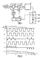
- FIG. 1 shows a PLL angle demodulator according to the invention having a signal input I for applying an angle-modulated input signal thereto and a signal output 01-03 from which the demodulated baseband angle modulation signal is delirered.
- the PLL angle demodulator has a limiter circuit 1 coupled to its signal input I, followed by a phase-locked loop 2-12 incorporating successively a phase detection arrangement 2, an amplifier circuit 5, a low-pass filter 6 coupled to the signal output 01-03, a voltage-controlled oscillator 9 supplying two oscillator signals in phase quadrature, the common mode signal which is in phase relative to the input signal at the central frequency of this input signal, being applied to a common mode output 10 and the signal which is in phase quadrature with the input signal at the central frequency being applied to a quadrature output 11, as well as a limiter circuit 12 arranged between the common mode output 10 and the phase detection arrangement 2.
- the phase-detection arrangement 2 has a first input 30, a second input 31, a third input 32 and an output 33.
- the phase detection arrangement 2 is further provided with a compensation circuit connected to the inputs 30 and 32 and a multiplier circuit 4 connected to the output of the compensation circuit 3 and the input 31.
- the compensation circuit 3 receives on the one hand an amplitude-limited angle-modulated input signal A from the limiter circuit 1 and on the other hand the amplitude-limited common mode or in-phase oscillator signal as a so-called further detection carrier B from the limiter circuit 12.
- the limiter circuits 1 and 12 have been adjusted in such a manner that the carriers A and B are amplitude-limited to mutually the same value.
- the carriers A and B are subtracted from each other in the compensation circuit 3 which results in a pulse-shaped signal C constituting an input signal for the multiplier circuit 4.
- the quadrature oscillator signal functioning as a so-called quadrature carrier D is applied to the multiplier circuit 4 from the quadrature output 11 of the voltage-controlled oscillator 9, which causes an error signal E upon multiplication by the pulse-shaped signal C.
- this error signal E is applied via the output 33 to the low-pass filter 6 in which the baseband angle-demodulator signal is obtained which is applied on the one hand to terminals 01, 02 and 03 of the signal output 01-03 for further signal processing and/or reproduction and on the other hand to the voltage-controlled oscillator 9 for a phase coupling of the loop with the input signal A.
- a further low-pass filter passing only the d.c. voltage component of the demodulated signal to the oscillator may be disposed between the low-pass filter 6 and the voltage controlled oscillator.
- the carriers A and B are mutually equal so that the signal C is zero in this period.
- the output signal E of the multiplier circuit 4 is therefore also zero and, unlike conventional PLL angle demodulators, it does not have a second order interference product. Since such periods may occur frequently and for a comparatively long time in normally occurring modulation signals, the interference reduction obtained by the compensation is consequently already considerable.
- pulses in successively alternating polarities occur in the signal C whose width indicates the absolute magnitude of the phase difference and whose polarity is determined by the polarity change resulting from the successive alternation of leading and trailing edges and the polarity of the phase difference.
- the polarity change of the pulses caused by the alternation in edge direction and the signal subtraction operation successively being effected in the compensation circuit C is eliminated due to multiplication of the signal C by the quadrature detection carrier D.
- the pulse series in the period 0-t1 then has a sign which is opposite relative to the pulse series in the period larger than t2, so that the polarity of the pulses is uniformly dependent on the polarity of the modulation signal.
- the 2nd order harmonic interference at 2f IN during these pulse series amounts approximately to 90 and is therefore considerably less than in the corresponding output signal of a phase detection arrangement of a conventional PLL angle demodulator.
- phase difference substantially occurs only when the modulation signal deviates from zero, the ratio between desired and undesired signal components in the output signal of the low-pass filter 6 being greatly improved relative to that in conventional PLL angle-demodulators, both in the case where 2f IN falls within and beyond the base frequency band of the modulation signal. This is particularly true of small amplitudes of the modulation signal.
- the baseband modulation signal F is selected, whilst possible higher order interference products falling beyond the base frequency band of the modulation signal are suppressed.
- the baseband modulation signal F is subsequently applied to the signal output 01-03.
- the amplifier circuit 5 includes a voltage current converter and the low-pass filter 6 is realized by means of a series arrangement of a resistor 7 coupled to a common connection between the amplifier circuit 5 and the voltage-controlled oscillator 9, and a capacitor 8 connected to ground, whilst the ends of these elements 7 and 8 are coupled to terminals 01, 02 and 03, respectively, of the signal output 01-03.
- the stereo difference signal (L-R) is available across the resistor 7, i.e. across the terminals 01 and 02
- the stereo sum signal (L+R) or the mono signal is available across the capacitor 8, i.e. 02 and 03
- the entire baseband stereo multiplex signal is available across the terminals 01 and 03.
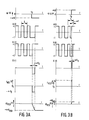
- the PLL angle demodulator described so far has an asymmetrical demodulation operation, which will be explained with reference to the graphs in Figures 3A en 3B.
- Figures 3A en 3B show the behaviour of the PLL angle demodulator and, for the sake of simplicity initially a situation without low-pass filter 6 (in the given case comparable to a situation in which the capacitor 8 has a, very high capacitance) for a negative phase variation - ⁇ ⁇ and a positive phase variation ⁇ ⁇ , respectively, of the input signal A(t) relative to the central carrier frequency f o occurring at t o .
- Figure 3A shows that the negative variation - ⁇ ⁇ results in a delay of the next zero crossing in the input signal A(t) after t o over a period ⁇ D relative to the corresponding zero crossing in the common mode detection carrier B(t).
- an error signal E(t) occurs at the output of the multiplier circuit 4 has a control signal for the voltage-controlled oscillator 9 and this error signal E(t) causes the oscillator frequency f VCO to decrease by ⁇ f D .
- This results in a decrease of the oscillator phase ⁇ VCO (t) by ⁇ ⁇ VCO ⁇ ⁇ . ⁇ D / f o .
- Figure 3B shows that the positive variation ⁇ ⁇ , whose magnitude is equal to the above-described negative variation - ⁇ ⁇ results in an earlier occurrence of the next zero crossing after t o in A(t) followed by an earlier occurrence of the corresponding zero crossing in B(t) after a control through the voltage-controlled oscillator 9. Since error signal E(t) as a control signal for the voltage-controlled oscillator 9 brings the oscillator frequency f VCO (t) to a value of f o + ⁇ f U immediately after the zero crossing in A(t), the duration of this error signal E(t), i.e.
- the duration between the said zero crossing in A(t) and the corresponding zero crossing in B(t) is: ⁇ U + ⁇ ⁇ / 2 ⁇ (f o + ⁇ f U ) which is shorter than ⁇ D .
- This polarity asymmetry is not disturbing or hardly disturbing for small phase variations, i.e. small amplitudes of the angle modulation signal.
- FIG 4 shows a practical embodiment of an asymmetric amplifier circuit 5 having a voltage signal input V in , a current signal output I out and a voltage reference input V REF for applying a threshold voltage.
- the voltage signal input V in is coupled to the output 33 of the phase detection arrangement 2 and receives the error signal E (t), whilst the current signal output I out is coupled via the resistor 7 to the capacitor 8 functioning as an integration capacitor of the low-pass filter 6.
- the amplifier circuit 5 has first and second threshold current source circuits (I U , 13-14) and (I D , 25-26) incorporating an emitter-coupled PNP transistor pair (13, 14), whose emitters are connected to a supply voltage via a common current source I U , and an emitter-coupled NPN transistor pair 25, 26, respectively, whose emitters are connected to ground via a common current source I D .
- the base electrodes of input transistors 13 and 25 of these two transistor pairs (13, 14) and (25, 26) are connected via a first DC voltage shift circuit 15-18 to the input V in , whilst the collectors of these input transistors are coupled to ground and to the supply voltage, respectively.
- Each d.c. voltage shift circuit (15-18) and (19-24) comprises a diode circuit (16, 17) and (20-23) whose anode connection is coupled at one end via current sources 15 and 19 to the supply voltage and at the other end to the base electrodes of the transistors 13 and 14 and whose cathodes connection is coupled via current sources 18 and 24 to ground at one end and to the base electrodes of the transistors 25 and 26 at the other end.
- the diode circuit 16, 17 comprises a series arrangement of two diodes 16 and 17 whose common connection is coupled to the voltage signal input V in .
- the diode circuit 20-23 comprises a series arrangement of four diodes 20 to 23 inclusive, whose common connection between the diodes 21 and 22 is coupled to the voltage reference input V REF .
- the base voltage of the input transistor 13 can exceed the first threshold voltage of the current source circuit (I U , 13-24) determined by the reference voltage and the voltages across the diodes 20 and 21 and the diode 16 so that the output transistor 14 starts conducting and applies the current from the current source I U as a so-called first current to the current signal output I out .
- the base voltage of the input transistor 25 may fall below the second threshold voltage determined by the reference voltage and the voltage across the diodes 17, 22 and 23, so that the output transistor 26 starts conducting and withdraws the current from the current source I D as a so-called second current from the current signal output I out .
- the current direction at the current output is thus dependent on the direction of the said angle variation.
- the magnitudes of the two currents have been mutually chosen in such a ratio that the asymmetry of the loop behaviour is compensated thereby.
- the current from the current source I U is to be chosen to be 5 times as large as that of the current source I D for this purpose.
- the amplifier circuit 5 does not supply a current signal in the range between the two threshold voltages, amplitude variations in the error signal E(t) which may be caused, for example, by an incomplete compensation in the compensation circuit 3 can be eliminated. As a result the influence of, for example, mutual deviations in the limitation levels of the limiter circuits 1 and 12 on the reliability of the demodulation operation is greatly reduced.
- FIG 5 shows an embodiment of an angle demodulator according to the invention which is applicable in a simple manner to conventional FM quadrature demodulators and whose elements corresponding to those of the PLL angle demodulator of Figure 1 have the same reference numerals.
- phase shifters 27 and 28 each realizing a frequency-dependent phase shift which is substantially 90° at the central frequency of the input signal.
- the first phase shifter 27 is coupled at one end to the limiter circuit 1 and at the other end to the second phase shifter 28 and via the input 31 of the phase detection arrangement 2 to the multiplier circuit 4.
- An output of the second phase shifter 28 is coupled via a limiter circuit 29 and via the input 32 of the phase detection arrangement 2 to the compensation circuit 3 which may be constituted in this case by an adder circuit due to the anti-phase relation of the detection carrier 3 relative to the input signal A at the central frequency.
- the input signal A is first compensated with the in-phase or anti-phase detection carrier B, the resulting signal E being subsequently multiplied by the quadrature detection carrier D.
- the quadrature detection carrier D When using a second multiplier, it is alternatively possible to multiply the input signal A and the further detection carrier B by the quadrature detection carrier D separately and to subsequently apply the output signals of the two multipliers to a compensation circuit. This is shown in Figure 6 in which element corresponding to those in Figures 1 and 5 have the same reference numerals.
- the carriers A and D are multiplied in a first multiplier 34, the carriers B and D are multiplied in a second multiplier 35, and the output signals of the two multipliers are applied to a compensation circuit 36 which applies the detected, but non-filtered signal E to the output 33.
- the compensation circuit is a subtractor circuit, whereas it is an adder circuit if the carriers are in anti-phase with each other.
- the central frequency the frequency located in the centre of the frequency spectrum of the angle-modulated input signal, as, for example, for audio modulation signals, but under given circumstances it may be desirable to choose a different frequency within this spectrum as a central frequency, for example, the frequency corresponding to the black level of the relevant video signal in the case of video modulation signals.
Landscapes
- Engineering & Computer Science (AREA)
- Power Engineering (AREA)
- Digital Transmission Methods That Use Modulated Carrier Waves (AREA)
Priority Applications (1)
| Application Number | Priority Date | Filing Date | Title |
|---|---|---|---|
| AT86201616T ATE60964T1 (de) | 1985-09-19 | 1986-09-17 | Winkeldemodulator. |
Applications Claiming Priority (4)
| Application Number | Priority Date | Filing Date | Title |
|---|---|---|---|
| NL8502562 | 1985-09-19 | ||
| NL8502562 | 1985-09-19 | ||
| NL8502967A NL8502967A (nl) | 1985-09-19 | 1985-10-30 | Hoekdemodulator. |
| NL8502967 | 1985-10-30 |
Publications (2)
| Publication Number | Publication Date |
|---|---|
| EP0217457A1 true EP0217457A1 (fr) | 1987-04-08 |
| EP0217457B1 EP0217457B1 (fr) | 1991-02-20 |
Family
ID=26646073
Family Applications (1)
| Application Number | Title | Priority Date | Filing Date |
|---|---|---|---|
| EP86201616A Expired EP0217457B1 (fr) | 1985-09-19 | 1986-09-17 | Démodulateur d'oscillations modulées en angle |
Country Status (6)
| Country | Link |
|---|---|
| US (1) | US4740759A (fr) |
| EP (1) | EP0217457B1 (fr) |
| AU (1) | AU585780B2 (fr) |
| CA (1) | CA1255365A (fr) |
| DE (1) | DE3677560D1 (fr) |
| NL (1) | NL8502967A (fr) |
Cited By (6)
| Publication number | Priority date | Publication date | Assignee | Title |
|---|---|---|---|---|
| EP0370539A1 (fr) * | 1988-10-14 | 1990-05-30 | Koninklijke Philips Electronics N.V. | Comparateur de phase et démodulateur de fréquence muni d'un tel comparateur de phase |
| RU2483430C2 (ru) * | 2011-08-02 | 2013-05-27 | Федеральное государственное военное образовательное учреждение высшего профессионального образования "Военный авиационный инженерный университет" (г. Воронеж) Министерства обороны Российской Федерации | Способ демодуляции и фильтрации фазомодулированных сигналов и устройство его реализации |
| RU2483432C2 (ru) * | 2011-08-03 | 2013-05-27 | Федеральное государственное военное образовательное учреждение высшего профессионального образования "Военный авиационный инженерный университет" (г. Воронеж) Министерства обороны Российской Федерации | Способ демодуляции фазомодулированных сигналов и устройство его реализации |
| RU2483433C2 (ru) * | 2011-08-04 | 2013-05-27 | Федеральное государственное военное образовательное учреждение высшего профессионального образования "Военный авиационный инженерный университет" (г. Воронеж) Министерства обороны Российской Федерации | Способ демодуляции фазомодулированных сигналов и устройство его реализации |
| RU2483431C2 (ru) * | 2011-08-03 | 2013-05-27 | Федеральное государственное военное образовательное учреждение высшего профессионального образования "Военный авиационный инженерный университет" (г. Воронеж) Министерства обороны Российской Федерации | Способ демодуляции и фильтрации фазомодулированных сигналов и устройство его реализации |
| RU2568389C1 (ru) * | 2014-10-21 | 2015-11-20 | Федеральное государственное казенное военное образовательное учреждение высшего профессионального образования "Военный учебно-научный центр Военно-воздушных сил "Военно-воздушная академия имени профессора Н.Е. Жуковского и Ю.А. Гагарина" (г. Воронеж) Министерства обороны Российской Федерации | Способ усиления и демодуляции частотно-модулированных сигналов и устройство его реализации |
Families Citing this family (2)
| Publication number | Priority date | Publication date | Assignee | Title |
|---|---|---|---|---|
| US5748049A (en) * | 1994-11-23 | 1998-05-05 | Anadigics, Inc. | Multi-frequency local oscillators |
| US20060028587A1 (en) * | 2004-08-05 | 2006-02-09 | Peng Juen T | TV tuner |
Citations (7)
| Publication number | Priority date | Publication date | Assignee | Title |
|---|---|---|---|---|
| US3564434A (en) * | 1968-07-29 | 1971-02-16 | Signetics Corp | Integrated frequency selective circuit and demodulator including phase locked loop |
| US3702442A (en) * | 1970-03-07 | 1972-11-07 | Philips Corp | Detection circuit for frequency-modulated signals |
| US3949314A (en) * | 1973-11-06 | 1976-04-06 | Sony Corporation | Phase demodulator |
| US4034309A (en) * | 1975-12-23 | 1977-07-05 | International Business Machines Corporation | Apparatus and method for phase synchronization |
| US4170023A (en) * | 1977-06-17 | 1979-10-02 | Sony Corporation | Carrier agc circuit, especially burst acc and apc |
| GB2080061A (en) * | 1980-07-02 | 1982-01-27 | Philips Electronic Associated | Amplifier circuit arrangement suitable for use in phase lock loop |
| GB2122827A (en) * | 1979-09-04 | 1984-01-18 | Philips Nv | Radio receiver including a muting circuit |
Family Cites Families (4)
| Publication number | Priority date | Publication date | Assignee | Title |
|---|---|---|---|---|
| NL184594C (nl) * | 1979-09-04 | 1989-09-01 | Philips Nv | Radio-ontvanger voorzien van een frequentie gesleutelde lus met audiofrequente terugkoppeling, en een stomschakeling. |
| FR2472878A1 (fr) * | 1979-12-27 | 1981-07-03 | Thomson Csf | Circuit pour la demodulation d'un signal module par une information numerique et recepteur comportant un tel circuit |
| US4476585A (en) * | 1982-01-25 | 1984-10-09 | International Telephone And Telegraph Corporation | Baseband demodulator for FM signals |
| AU5104085A (en) * | 1985-12-10 | 1987-06-11 | International Standard Electric Corp. | Fm/am demodulation |
-
1985
- 1985-10-30 NL NL8502967A patent/NL8502967A/nl not_active Application Discontinuation
-
1986
- 1986-09-16 AU AU62713/86A patent/AU585780B2/en not_active Ceased
- 1986-09-17 DE DE8686201616T patent/DE3677560D1/de not_active Expired - Lifetime
- 1986-09-17 EP EP86201616A patent/EP0217457B1/fr not_active Expired
- 1986-09-18 CA CA000518579A patent/CA1255365A/fr not_active Expired
- 1986-09-19 US US06/909,655 patent/US4740759A/en not_active Expired - Fee Related
Patent Citations (7)
| Publication number | Priority date | Publication date | Assignee | Title |
|---|---|---|---|---|
| US3564434A (en) * | 1968-07-29 | 1971-02-16 | Signetics Corp | Integrated frequency selective circuit and demodulator including phase locked loop |
| US3702442A (en) * | 1970-03-07 | 1972-11-07 | Philips Corp | Detection circuit for frequency-modulated signals |
| US3949314A (en) * | 1973-11-06 | 1976-04-06 | Sony Corporation | Phase demodulator |
| US4034309A (en) * | 1975-12-23 | 1977-07-05 | International Business Machines Corporation | Apparatus and method for phase synchronization |
| US4170023A (en) * | 1977-06-17 | 1979-10-02 | Sony Corporation | Carrier agc circuit, especially burst acc and apc |
| GB2122827A (en) * | 1979-09-04 | 1984-01-18 | Philips Nv | Radio receiver including a muting circuit |
| GB2080061A (en) * | 1980-07-02 | 1982-01-27 | Philips Electronic Associated | Amplifier circuit arrangement suitable for use in phase lock loop |
Non-Patent Citations (1)
| Title |
|---|
| PROCEEDINGS OF THE IEEE, vol. 63, no. 2, February 1975, pages 291-306, New York, US; S.C.GUPTA: "Phase-locked loops" * |
Cited By (6)
| Publication number | Priority date | Publication date | Assignee | Title |
|---|---|---|---|---|
| EP0370539A1 (fr) * | 1988-10-14 | 1990-05-30 | Koninklijke Philips Electronics N.V. | Comparateur de phase et démodulateur de fréquence muni d'un tel comparateur de phase |
| RU2483430C2 (ru) * | 2011-08-02 | 2013-05-27 | Федеральное государственное военное образовательное учреждение высшего профессионального образования "Военный авиационный инженерный университет" (г. Воронеж) Министерства обороны Российской Федерации | Способ демодуляции и фильтрации фазомодулированных сигналов и устройство его реализации |
| RU2483432C2 (ru) * | 2011-08-03 | 2013-05-27 | Федеральное государственное военное образовательное учреждение высшего профессионального образования "Военный авиационный инженерный университет" (г. Воронеж) Министерства обороны Российской Федерации | Способ демодуляции фазомодулированных сигналов и устройство его реализации |
| RU2483431C2 (ru) * | 2011-08-03 | 2013-05-27 | Федеральное государственное военное образовательное учреждение высшего профессионального образования "Военный авиационный инженерный университет" (г. Воронеж) Министерства обороны Российской Федерации | Способ демодуляции и фильтрации фазомодулированных сигналов и устройство его реализации |
| RU2483433C2 (ru) * | 2011-08-04 | 2013-05-27 | Федеральное государственное военное образовательное учреждение высшего профессионального образования "Военный авиационный инженерный университет" (г. Воронеж) Министерства обороны Российской Федерации | Способ демодуляции фазомодулированных сигналов и устройство его реализации |
| RU2568389C1 (ru) * | 2014-10-21 | 2015-11-20 | Федеральное государственное казенное военное образовательное учреждение высшего профессионального образования "Военный учебно-научный центр Военно-воздушных сил "Военно-воздушная академия имени профессора Н.Е. Жуковского и Ю.А. Гагарина" (г. Воронеж) Министерства обороны Российской Федерации | Способ усиления и демодуляции частотно-модулированных сигналов и устройство его реализации |
Also Published As
| Publication number | Publication date |
|---|---|
| NL8502967A (nl) | 1987-04-16 |
| AU585780B2 (en) | 1989-06-22 |
| CA1255365A (fr) | 1989-06-06 |
| DE3677560D1 (de) | 1991-03-28 |
| EP0217457B1 (fr) | 1991-02-20 |
| US4740759A (en) | 1988-04-26 |
| AU6271386A (en) | 1987-03-26 |
Similar Documents
| Publication | Publication Date | Title |
|---|---|---|
| EP0160339B1 (fr) | Récepteur de données FM à modulation directe | |
| EP0184873B1 (fr) | Boucle d'asservissement de phase, notamment pour l'utilisation dans un récepteur synchrone AM à mélange direct | |
| JPS583424B2 (ja) | ステレオフクゴウシンゴウハツセイホウホウ オヨビ ソウチ | |
| EP0217457B1 (fr) | Démodulateur d'oscillations modulées en angle | |
| US4103244A (en) | Fsk demodulator | |
| US4970469A (en) | Phase detector and frequency demodulator including such a phase detector | |
| US5014316A (en) | Compatible quadrature amplitude modulation detector system | |
| JPS6347307B2 (fr) | ||
| EP0484914B1 (fr) | Démodulateur et procédé de démodulation pour signaux numériques modulés en MSK | |
| US4502148A (en) | FM Stereo demodulator for demodulating stereo signals directly from an FM intermediate frequency signal | |
| US4511849A (en) | FM Pulse counting demodulator with multiplier for input and delayed input signals | |
| JP2964573B2 (ja) | コスタスループ搬送波再生回路 | |
| JPH06105892B2 (ja) | 制御発振器 | |
| US5323242A (en) | Carrier signal generating circuit in video signal recording/reproducing apparatus | |
| JPH0461450A (ja) | 遅延検波回路 | |
| JPH0557781B2 (fr) | ||
| GB2369755A (en) | Circuit for the demodulation of the logic signal transmitted by analog channels | |
| US6985541B1 (en) | FM demodulator for a low IF receiver | |
| US5526061A (en) | Circuit arrangement for demodulating a video signal | |
| JPS6267904A (ja) | 角度復調器 | |
| JPH0219664B2 (fr) | ||
| JP2626102B2 (ja) | Fm復調器 | |
| EP1236271B1 (fr) | Demodulateur mf utilisant des monostables | |
| JPH0423543A (ja) | 4相差動位相変調復調回路 | |
| JPH0129471B2 (fr) |
Legal Events
| Date | Code | Title | Description |
|---|---|---|---|
| PUAI | Public reference made under article 153(3) epc to a published international application that has entered the european phase |
Free format text: ORIGINAL CODE: 0009012 |
|
| AK | Designated contracting states |
Kind code of ref document: A1 Designated state(s): AT BE DE FR GB IT NL SE |
|
| 17P | Request for examination filed |
Effective date: 19871001 |
|
| 17Q | First examination report despatched |
Effective date: 19890718 |
|
| GRAA | (expected) grant |
Free format text: ORIGINAL CODE: 0009210 |
|
| AK | Designated contracting states |
Kind code of ref document: B1 Designated state(s): AT BE DE FR GB IT NL SE |
|
| PG25 | Lapsed in a contracting state [announced via postgrant information from national office to epo] |
Ref country code: IT Free format text: LAPSE BECAUSE OF FAILURE TO SUBMIT A TRANSLATION OF THE DESCRIPTION OR TO PAY THE FEE WITHIN THE PRE;WARNING: LAPSES OF ITALIAN PATENTS WITH EFFECTIVE DATE BEFORE 2007 MAY HAVE OCCURRED AT ANY TIME BEFORE 2007. THE CORRECT EFFECTIVE DATE MAY BE DIFFERENT FROM THE ONE RECORDED.SCRIBED TIME-LIMIT Effective date: 19910220 Ref country code: NL Effective date: 19910220 Ref country code: FR Effective date: 19910220 Ref country code: SE Effective date: 19910220 Ref country code: AT Effective date: 19910220 Ref country code: BE Effective date: 19910220 |
|
| REF | Corresponds to: |
Ref document number: 60964 Country of ref document: AT Date of ref document: 19910315 Kind code of ref document: T |
|
| REF | Corresponds to: |
Ref document number: 3677560 Country of ref document: DE Date of ref document: 19910328 |
|
| EN | Fr: translation not filed | ||
| NLV1 | Nl: lapsed or annulled due to failure to fulfill the requirements of art. 29p and 29m of the patents act | ||
| PG25 | Lapsed in a contracting state [announced via postgrant information from national office to epo] |
Ref country code: GB Effective date: 19910917 |
|
| PLBE | No opposition filed within time limit |
Free format text: ORIGINAL CODE: 0009261 |
|
| STAA | Information on the status of an ep patent application or granted ep patent |
Free format text: STATUS: NO OPPOSITION FILED WITHIN TIME LIMIT |
|
| 26N | No opposition filed | ||
| GBPC | Gb: european patent ceased through non-payment of renewal fee | ||
| PG25 | Lapsed in a contracting state [announced via postgrant information from national office to epo] |
Ref country code: DE Effective date: 19920602 |